EP0533191A2 - PSK-Demodulator mit Frequenzmultiplikation zur Phasen- und Frequenzkorrektur - Google Patents
PSK-Demodulator mit Frequenzmultiplikation zur Phasen- und Frequenzkorrektur Download PDFInfo
- Publication number
- EP0533191A2 EP0533191A2 EP92116016A EP92116016A EP0533191A2 EP 0533191 A2 EP0533191 A2 EP 0533191A2 EP 92116016 A EP92116016 A EP 92116016A EP 92116016 A EP92116016 A EP 92116016A EP 0533191 A2 EP0533191 A2 EP 0533191A2
- Authority
- EP
- European Patent Office
- Prior art keywords
- signal
- complex
- circuit
- multiplier
- frequency
- Prior art date
- Legal status (The legal status is an assumption and is not a legal conclusion. Google has not performed a legal analysis and makes no representation as to the accuracy of the status listed.)
- Granted
Links
Images


Classifications
-
- H—ELECTRICITY
- H04—ELECTRIC COMMUNICATION TECHNIQUE
- H04L—TRANSMISSION OF DIGITAL INFORMATION, e.g. TELEGRAPHIC COMMUNICATION
- H04L27/00—Modulated-carrier systems
- H04L27/18—Phase-modulated carrier systems, i.e. using phase-shift keying
- H04L27/22—Demodulator circuits; Receiver circuits
- H04L27/233—Demodulator circuits; Receiver circuits using non-coherent demodulation
- H04L27/2332—Demodulator circuits; Receiver circuits using non-coherent demodulation using a non-coherent carrier
-
- H—ELECTRICITY
- H04—ELECTRIC COMMUNICATION TECHNIQUE
- H04L—TRANSMISSION OF DIGITAL INFORMATION, e.g. TELEGRAPHIC COMMUNICATION
- H04L27/00—Modulated-carrier systems
- H04L27/0014—Carrier regulation
- H04L2027/0024—Carrier regulation at the receiver end
- H04L2027/0026—Correction of carrier offset
- H04L2027/003—Correction of carrier offset at baseband only
-
- H—ELECTRICITY
- H04—ELECTRIC COMMUNICATION TECHNIQUE
- H04L—TRANSMISSION OF DIGITAL INFORMATION, e.g. TELEGRAPHIC COMMUNICATION
- H04L27/00—Modulated-carrier systems
- H04L27/0014—Carrier regulation
- H04L2027/0044—Control loops for carrier regulation
- H04L2027/0046—Open loops
- H04L2027/0048—Frequency multiplication
Definitions
- This invention relates to a demodulator circuit and, in particular, to a synchronous-detection demodulator circuit which is widely used in various communication systems, for example, in a mobile communication system.
- the modem comprises modulator and demodulator circuits which will be described in the following.
- the modulator circuit is for modulating an original analog signal by phase-modulating a plurality of phases of a particular number into a modulated signal having a particular frequency.
- the modulated signal is used as a carrier in the mobile communication system in the manner known in the art.
- the demodulator circuit is for demodulating the modulated signal into a demodulated signal.
- the demodulated signal is a reproduction of the original analog signal.
- a conventional demodulator circuit comprises a signal converting circuit, a frequency multiplier, a signal processing circuit, a frequency demultiplier, and a signal producing circuit.
- the signal converting circuit is for converting the modulated signal into a digital signal.
- the frequency multiplier is for multiplying the particular frequency by the particular number to produce a multiplied signal.
- the signal processing circuit is for processing the multiplied signal into a modified signal of a multiplied frequency.
- the frequency demultiplier is for demultiplying the multiplied frequency by the particular number to produce a demultiplied signal of the particular frequency.
- the signal producing circuit is for producing the demodulated signal in accordance with the digital and the demultiplied signals.
- the conventional demodulator circuit has a disadvantage in that it is difficult to continuously and accurately carry out demodulating operation as will later be discussed in detail.
- a demodulator circuit for demodulating a modulated signal into a demodulated signal.
- the modulated signal is derived by phase-modulating in m phases an original analog signal and having a particular frequency.
- the demodulated signal is a reproduction of the analog signal.
- the demodulator circuit comprises a signal converting circuit for converting the modulated signal into a digital signal, a frequency multiplier for multiplying the particular frequency by m to produce a multiplied signal, a signal processing circuit for processing the multiplied signal into a modified signal of a multiplied frequency, a frequency demultiplier for demultiplying the multiplied frequency by m to produce a demultiplied signal of the particular frequency, and a signal producing circuit for producing the demodulated signal in accordance with the digital and the demultiplied signals.
- the signal processing circuit comprises a complex clock signal generator for generating a complex clock signal representing a first complex number and having a frequency which is substantially equal to the particular frequency, a local complex signal producing circuit for producing a complex local signal representing a second complex number, a first signal processing circuit connected to the frequency multiplier into a first processed signal, a second signal processing circuit connected to the frequency multiplier for processing the multiplied signal into a second processed signal in accordance with a conjugate complex clock signal supplied from the complex clock signal generator and with the complex local signal supplied from the local complex signal producing circuit, a third signal processing circuit connected to the frequency multiplier for processing the multiplied signal into a third processed signal in accordance with the complex clock signal supplied from the complex clock signal generator and with a conjugate complex local signal supplied from the local complex signal producing circuit, an adder connected to the first, the second, and the third signal processing circuits for summing up the first, the second, and the third processed signals into a sum signal, and supply means connected to the frequency demultiplier and the adder for supplying the
- the conventional demodulator circuit is for demodulating a modulated signal into a demodulated signal.
- the modulated signal is derived by phase-modulating in m phases an original analog signal and having a particular frequency, where m represents a predetermined number.
- the demodulated signal is a reproduction of the analog signal.
- the demodulator circuit comprises a signal converting circuit 11, a frequency multiplier 12, a signal processing circuit 13, a frequency demultiplier 14, and a signal producing circuit 15, each of which will be described in the following.
- the signal converting circuit 11 is for converting the modulated signal into a digital signal and will later be described in detail.
- the frequency multiplier 12 is connected to the signal converting circuit 11 and is for multiplying the particular frequency by m to produce a frequency multiplied signal.
- the signal processing circuit 13 is connected to the frequency multiplier 12 and is for processing the multiplied signal into a modified signal of a multiplied frequency.
- the frequency demultiplier 14 is connected to the signal processing circuit 13 and is for demultiplying the multiplied frequency by m to produce a frequency demultiplied signal of the particular frequency.
- the signal producing circuit 15 is connected to the signal converting circuit 11 and the frequency demultiplier 14 and is for producing the demodulated signal in accordance with the digital and the demultiplied signals.
- the signal converting circuit 11 comprises a complex local oscillator 16, a ⁇ /2-phase shifter 17, a first mixer 18, a second mixer 19, a first low-pass filter 21, a second low-pass filter 22, a first A/D converter 23, a second A/D converter 24, and a timing clock generator 25, each of which will be described in the following.
- the complex local oscillator 16 is for generating a cosine-sine wave signal having a specific frequency substantially equal to the particular frequency of the modulated signal.
- the cosine-sine wave signal is supplied as a first wave signal to a first mixer 18 directly and as a second wave signal to the second mixer 19 through the ⁇ /2 phase shifter 17.
- Each of the first and the second mixers 18 and 19 is supplied with the modulated signal that is represented as follows: where ⁇ c represents the particular frequency, ⁇ c representing a particular phase of the modulated signal. It is to be noted that ⁇ L and ⁇ c are substantially equal to each other.
- the first mixer 18 is for frequency-converting the modulated signal into a first baseband complex signal with reference to the first wave signal.
- the second mixer 19 is for frequency-converting the modulated signal into a second baseband complex signal with reference to the second wave signal.
- the first and the second low-pass filters 21 and 22 Responsive to the first and the second baseband complex signals, the first and the second low-pass filters 21 and 22 produce a first and a second filtered complex signal, respectively. In particular, the first and the second low-pass filters 21 and 22 delete the second term on the righthand side of Equation (3).
- the first A/D converter 23 is for converting the first filtered complex signal into a first converted signal with reference to a sample timing clock signal which is supplied from the timing clock generator 25.
- the second A/D converter 24 is for converting the second filtered complex signal into a second converted signal with reference to the sample timing clock signal supplied from the timing clock generator 25.
- the frequency multiplier 12 multiplies the digital signal V R (t) of Equation (4) by m to produce the multiplied signal.
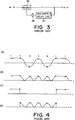
- the multiplied signal has a plurality of line spectrum components which is produced as exemplified in Fig. 2.
- the multiplied signal has a DC component and a clock component and is generally represented as follows: where a(t) represents an amplitude of the DC component, a combination of b(t) and c(t) representing an amplitude of the clock component.
- the signal processing circuit 13 comprises an adder 26, a one-sample delay unit 27, and an ⁇ -multiplier 28 which are collectively operable as a low-pass filter in the manner known in the art.
- the signal processing circuit 13 carries out low-pass operation which is represented by the following Equation (9) except for coefficients.
- the frequency multiplier 12 multiplies the digital signal by m, namely, 2 to produce the multiplied signal illustrated along a second row labelled (B).
- the multiplied signal can be separated into the DC component and the clock component.
- the DC component is illustrated along a third row labelled (C).
- the clock component is illustrated along a fourth or bottom row labelled (D). It is to be noted that the multiplied signal appears in response to the DC component and that the DC component is not continuous in the third row (C). This means that the demodulated signal is interrupted when the clock component continuously appears during a long time.
- the demodulated signal In order to continuously produce the demodulated signal, it is necessary to make ⁇ of Equation (9) be relatively great. However, the demodulated signal has a phase error when a great number is selected as ⁇ of Equation (9). When the phase error is great, the demodulated signal has an error.
- Fig. 5 the description will be directed to a demodulator circuit according to a preferred embodiment of this invention.
- the demodulator circuit comprises similar parts designated by like reference numerals.
- the signal processing circuit 13 comprises a complex clock signal generator 28 and a local complex signal producing circuit 29.
- the complex clock signal generator 28 is for generating a complex clock signal representing a first complex number and having a frequency which is substantially equal to the particular frequency.
- the signal processing circuit 13 further comprises first, second, and third signal processing circuits 31, 32, and 33 and an adder 34 each of which will be described in the following.
- the second signal processing circuit 32 is connected to the frequency multiplier 12, the complex clock signal generator 28, and the local complex signal producing circuit 29 and is for processing the multiplied signal into a second processed signal in accordance with the complex local signal and a conjugate complex clock signal which represents a complex conjugate of the first complex number. It is readily possible to make the complex clock signal generator 28 generate the complex clock signal as well as the conjugate complex clock signal. The second processed signal will become clear from the following description.
- the second signal processing circuit 32 comprises a first multiplier 36, a first tank circuit 37, and a second multiplier 38.
- the second multiplier 38 is connected to the local complex signal producing and the first tank circuits 29 and 37 and is for multiplying the complex local signal by the first filtered signal to produce a second product signal which is represented as follows:
- the second product signal is supplied as the second processed signal to the adder 34 through a line 39 which may be referred to as a first local supply arrangement.
- the third signal processing circuit 33 is connected to the frequency multiplier 12, the complex clock signal generator 28, and the local complex signal producing circuit 29 and is for processing the multiplied signal into a third processed signal in accordance with the complex clock signal and a conjugate complex local signal which represents a complex conjugate of the second complex number.
- the third processed signal will be clear from the following description.
- the third signal processing circuit 33 comprises a third multiplier 41, a second tank circuit 42, and a fourth multiplier 43.
- the third multiplier 41 is connected to the frequency multiplier 12 and the complex clock signal generator 28 and is for multiplying the multiplied signal by the complex clock signal to produce a third product signal which is represented as follows:
- the fourth multiplier 43 is connected to the local complex signal producing and the fourth tank circuits 29 and 42 and is for multiplying the conjugate complex local signal by the second filtered signal to produce a fourth product signal which is represented as follows:
- the fourth product signal is supplied as the third processed signal to the adder 34 through a line 44 which may be referred to as a second local supply arrangement.
- the adder 34 is for summing up the first, the second, and the third processed signals into a sum signal which is represented as follows:
- the sum signal is supplied as the modified signal to the demultiplier 14 through a line 45 which may be referred to as a supply arrangement.
- the description will be directed to the local complex signal producing circuit 29.
- the local complex signal producing circuit 29 comprises a first correlation detector 51, a second correlation detector 52, an additional adder 53, a low-pass filter 54, and a complex hard limiter 55, each of which will be described in the following. It is to be noted herein that the sum signal represents a particular complex number, the first processed local signal representing a first specific complex number, the first filtered signal representing a second specific complex number.
- the first correlation detector 51 is connected to the afore-mentioned adder 34 and the first tank circuit 37 and is for multiplying the sum signal supplied from the adder 34 by a conjugate first filtered signal supplied from the first tank circuit to produce a first correlation signal.
- the conjugate first filtered signal represents a complex conjugate of the first filtered signal.
- the first correlation signal is represented as follows:
- the second correlation detector 52 is connected to the adder 34 and the second tank circuit 42 and is for multiplying a conjugate sum signal supplied from the adder 34 by the second filtered signal supplied from the second tank circuit 42 to produce a second correlation signal.
- the conjugate sum signal represents a complex conjugate of the sum signal.
- the second correlation signal is represented as follows:
- the additional adder 53 is connected to the first and the second correlation detectors 51 and 52 and is for summing up the first and the second correlation signals into an additional sum signal which is represented as follows:
- the low-pass filter 54 is connected to the additional adder 53 and is for carrying out an averaging operation of the additional sum signal to produce an averaged signal having an amplitude representative of a result of the averaging operation.
- Equation (29) ⁇ Ke is very small. Accordingly, Equation (28) is rewritten into: e j ⁇ m (t) ⁇ (b2 + c2)e j ⁇ + a(b + c) + 2bce -j ⁇ .
- e 1 ⁇ represents a phase component of the averaged signal, where ⁇ ⁇ 1.
- phase error ⁇ -arctan ⁇ Ke D/(1 - ⁇ ).
- the limited signal represents a second complex number and may therefore be called herein the complex local signal.
- the complex hard limiter 55 carries out a predetermined calculation in accordance with the complex local signal to produce the conjugate complex local signal as a result of the predetermined calculation in the manner known in the art.
- the complex local signal is supplied to the second multiplier 38 through a line 56 which will be referred to as a first additional supply arrangement.
- the conjugate complex local signal is supplied to the fourth multiplier 43 through a line 57 which will be referred to as a second additional supply arrangement.
- the signal processing circuit 13 further comprises an additional multiplier 58 connected to the complex clock signal generator 28 and the low-pass filter 54.
- the additional multiplier 58 is for multiplying the complex clock signal by the averaged signal to produce a particular clock signal which represents the above-mentioned clock component.
- Equation (22) is rewritten into:
- Equation (35) is rewritten into: V16(t) ⁇ (a + b +c)e j(m ⁇ R t+m ⁇ R -arctan(m ⁇ R ⁇ )) .
- m is constant, a represents nonzero.
- the m is increased, b represents nonzero.
- the m is decreased, c represents nonzero. Accordingly, (a + b + c) is not equal to zero.
- the DC component is obtained regardless of the value of m.
- the clock component is present in a stable form in a case where both of b and c are not zero, namely, where the modulated signal has a change point therein. Accordingly, the DC component is produced by using the stable form of the clock component even when the clock component is present.
- each of the first signal processing, the first tank, and the second tank circuits 31, 37, and 42 may be a low-pass filter in the manner known in the art.
Landscapes
- Engineering & Computer Science (AREA)
- Computer Networks & Wireless Communication (AREA)
- Signal Processing (AREA)
- Digital Transmission Methods That Use Modulated Carrier Waves (AREA)
- Amplitude Modulation (AREA)
- Stabilization Of Oscillater, Synchronisation, Frequency Synthesizers (AREA)
Applications Claiming Priority (3)
| Application Number | Priority Date | Filing Date | Title |
|---|---|---|---|
| JP3239969A JP2765601B2 (ja) | 1991-09-19 | 1991-09-19 | 復調回路 |
| JP239969/91 | 1991-09-19 | ||
| JP23996991 | 1991-09-19 |
Publications (3)
| Publication Number | Publication Date |
|---|---|
| EP0533191A2 true EP0533191A2 (de) | 1993-03-24 |
| EP0533191A3 EP0533191A3 (en) | 1993-08-04 |
| EP0533191B1 EP0533191B1 (de) | 2005-03-02 |
Family
ID=17052530
Family Applications (1)
| Application Number | Title | Priority Date | Filing Date |
|---|---|---|---|
| EP92116016A Expired - Lifetime EP0533191B1 (de) | 1991-09-19 | 1992-09-18 | PSK-Demodulator mit Frequenzmultiplikation zur Phasen- und Frequenzkorrektur |
Country Status (6)
| Country | Link |
|---|---|
| US (1) | US5270665A (de) |
| EP (1) | EP0533191B1 (de) |
| JP (1) | JP2765601B2 (de) |
| AU (1) | AU656100B2 (de) |
| CA (1) | CA2078636C (de) |
| DE (1) | DE69233486T2 (de) |
Cited By (1)
| Publication number | Priority date | Publication date | Assignee | Title |
|---|---|---|---|---|
| EP0671838A2 (de) * | 1994-03-09 | 1995-09-13 | Martin Marietta Corporation | DPSK-Empfänger mit Kompensation des Dopplereffektes |
Families Citing this family (2)
| Publication number | Priority date | Publication date | Assignee | Title |
|---|---|---|---|---|
| US6023491A (en) * | 1994-06-21 | 2000-02-08 | Matsushita Electric Industrail Co., Ltd. | Demodulation apparatus performing different frequency control functions using separately provided oscillators |
| CA2230589C (en) * | 1998-02-25 | 2004-02-10 | Wen Tong | Determining sir in a communications system |
Citations (3)
| Publication number | Priority date | Publication date | Assignee | Title |
|---|---|---|---|---|
| FR2417888A1 (fr) * | 1978-02-17 | 1979-09-14 | Marconi Co Ltd | Demodulateur pour signal a modulation de phase a plusieurs niveaux |
| US4466108A (en) * | 1981-10-06 | 1984-08-14 | Communications Satellite Corporation | TDMA/PSK Carrier synchronization without preamble |
| EP0355587A2 (de) * | 1988-08-15 | 1990-02-28 | Nortel Networks Corporation | Takt- und Trägerrückgewinnung für TDMA ohne Präambelfolge |
Family Cites Families (1)
| Publication number | Priority date | Publication date | Assignee | Title |
|---|---|---|---|---|
| CA2018855C (en) * | 1989-06-14 | 1993-09-21 | Shousei Yoshida | Burst demodulator for establishing carrier and clock timing from a sequence of alternating symbols |
-
1991
- 1991-09-19 JP JP3239969A patent/JP2765601B2/ja not_active Expired - Fee Related
-
1992
- 1992-09-18 DE DE69233486T patent/DE69233486T2/de not_active Expired - Fee Related
- 1992-09-18 EP EP92116016A patent/EP0533191B1/de not_active Expired - Lifetime
- 1992-09-18 CA CA002078636A patent/CA2078636C/en not_active Expired - Fee Related
- 1992-09-21 US US07/947,603 patent/US5270665A/en not_active Expired - Fee Related
- 1992-09-22 AU AU25313/92A patent/AU656100B2/en not_active Ceased
Patent Citations (3)
| Publication number | Priority date | Publication date | Assignee | Title |
|---|---|---|---|---|
| FR2417888A1 (fr) * | 1978-02-17 | 1979-09-14 | Marconi Co Ltd | Demodulateur pour signal a modulation de phase a plusieurs niveaux |
| US4466108A (en) * | 1981-10-06 | 1984-08-14 | Communications Satellite Corporation | TDMA/PSK Carrier synchronization without preamble |
| EP0355587A2 (de) * | 1988-08-15 | 1990-02-28 | Nortel Networks Corporation | Takt- und Trägerrückgewinnung für TDMA ohne Präambelfolge |
Non-Patent Citations (2)
| Title |
|---|
| ELECTRONICS AND COMMUNICATIONS IN JAPAN - PART I, vol. 73, no. 6, June 1990, NEW YORK, US, pages 41 - 51 TOMOKI OHSAWA: 'BLOCK DEMODULATION METHOD FOR PSK SIGNAL BY SEQUENTIAL REGRESSION ESTIMATOR' * |
| IEEE INTERNATIONAL SYMPOSIUM ON CIRCUITS AND SYSTEMS, 7-9 JUNE 1988, ESPOO, FINLAND, vol. 2, pages 1815 - 1818 EGLIN P. ET AL.: 'DIGITAL IMPLEMENTATION OF A COHERENT CPM SYSTEM FOR MOBILE RADIO' * |
Cited By (2)
| Publication number | Priority date | Publication date | Assignee | Title |
|---|---|---|---|---|
| EP0671838A2 (de) * | 1994-03-09 | 1995-09-13 | Martin Marietta Corporation | DPSK-Empfänger mit Kompensation des Dopplereffektes |
| EP0671838A3 (de) * | 1994-03-09 | 1998-10-28 | Lockheed Martin Corporation | DPSK-Empfänger mit Kompensation des Dopplereffektes |
Also Published As
| Publication number | Publication date |
|---|---|
| AU656100B2 (en) | 1995-01-19 |
| CA2078636C (en) | 1998-05-26 |
| DE69233486D1 (de) | 2005-04-07 |
| EP0533191B1 (de) | 2005-03-02 |
| CA2078636A1 (en) | 1993-03-20 |
| US5270665A (en) | 1993-12-14 |
| EP0533191A3 (en) | 1993-08-04 |
| JPH0583314A (ja) | 1993-04-02 |
| AU2531392A (en) | 1993-03-25 |
| DE69233486T2 (de) | 2005-07-28 |
| JP2765601B2 (ja) | 1998-06-18 |
Similar Documents
| Publication | Publication Date | Title |
|---|---|---|
| US6067329A (en) | VSB demodulator | |
| EP0526833B1 (de) | Trägerfrequenz-Fehlerdetektorschaltung zur genauen Feststellung eines Trägerfrequenzfehlers | |
| JP3017041B2 (ja) | 自動周波数制御方法及びその装置 | |
| EP0675606A1 (de) | Empfänger für spreizspektrumübertragung | |
| EP0533208B1 (de) | PSK-Demodulator mit Rückkopplungsschaltung zur Phasen- und Frequenzkorrektur | |
| US5581582A (en) | Automatic frequency control method and apparatus therefor | |
| US4802191A (en) | Data transmission using a transparent tone-in band system | |
| US5914985A (en) | Digital demodulator | |
| US5090027A (en) | Coherent PSK demodulator with adaptive line enhancer | |
| EP0059415B1 (de) | System zur Demodulation von phasengetasteten Trägerfrequenzen | |
| EP0486839B1 (de) | Quasi-kohärenter MPSK-Demodulator | |
| US6204726B1 (en) | Digital demodulator | |
| EP0533191A2 (de) | PSK-Demodulator mit Frequenzmultiplikation zur Phasen- und Frequenzkorrektur | |
| US5867059A (en) | Demodulating system for MSK and GMSK signal using a fast fourier transform converter | |
| US4614910A (en) | Quarternary differential PSK demodulator | |
| JP2994836B2 (ja) | 復調器のafc回路 | |
| EP0535638B1 (de) | Phasenteiler für komplexe Signale | |
| EP1111866A1 (de) | Schaltung zur trägerwiedergabe | |
| KR0157498B1 (ko) | 자동주파수조절장치 | |
| JP2843699B2 (ja) | デジタル化直交変調器 | |
| JP3519365B2 (ja) | エネルギ分散されたqpsk信号の搬送波に対する簡単な同期化の支援のための方法 | |
| KR0157499B1 (ko) | 자동주파수조절방법 및 그 장치 | |
| JPH06105898B2 (ja) | 干渉補償回路 | |
| JP3382892B2 (ja) | 階層化伝送における位相変調信号をデジタル復調してフレーム同期パターン検出を行う方法及びその装置 | |
| EP0154963A2 (de) | Demodulator für vierphasendifferenzmodulierte Signale |
Legal Events
| Date | Code | Title | Description |
|---|---|---|---|
| PUAI | Public reference made under article 153(3) epc to a published international application that has entered the european phase |
Free format text: ORIGINAL CODE: 0009012 |
|
| AK | Designated contracting states |
Kind code of ref document: A2 Designated state(s): DE FR GB |
|
| PUAL | Search report despatched |
Free format text: ORIGINAL CODE: 0009013 |
|
| RHK1 | Main classification (correction) |
Ipc: H04L 27/22 |
|
| AK | Designated contracting states |
Kind code of ref document: A3 Designated state(s): DE FR GB |
|
| 17P | Request for examination filed |
Effective date: 19930618 |
|
| 17Q | First examination report despatched |
Effective date: 19991028 |
|
| GRAG | Despatch of communication of intention to grant |
Free format text: ORIGINAL CODE: EPIDOS AGRA |
|
| GRAG | Despatch of communication of intention to grant |
Free format text: ORIGINAL CODE: EPIDOS AGRA |
|
| GRAG | Despatch of communication of intention to grant |
Free format text: ORIGINAL CODE: EPIDOS AGRA |
|
| GRAH | Despatch of communication of intention to grant a patent |
Free format text: ORIGINAL CODE: EPIDOS IGRA |
|
| GRAH | Despatch of communication of intention to grant a patent |
Free format text: ORIGINAL CODE: EPIDOS IGRA |
|
| GRAA | (expected) grant |
Free format text: ORIGINAL CODE: 0009210 |
|
| AK | Designated contracting states |
Kind code of ref document: B1 Designated state(s): DE FR GB |
|
| PG25 | Lapsed in a contracting state [announced via postgrant information from national office to epo] |
Ref country code: FR Free format text: LAPSE BECAUSE OF NON-PAYMENT OF DUE FEES Effective date: 20050302 |
|
| REG | Reference to a national code |
Ref country code: GB Ref legal event code: FG4D |
|
| REF | Corresponds to: |
Ref document number: 69233486 Country of ref document: DE Date of ref document: 20050407 Kind code of ref document: P |
|
| PG25 | Lapsed in a contracting state [announced via postgrant information from national office to epo] |
Ref country code: GB Free format text: LAPSE BECAUSE OF NON-PAYMENT OF DUE FEES Effective date: 20050918 |
|
| PGFP | Annual fee paid to national office [announced via postgrant information from national office to epo] |
Ref country code: FR Payment date: 20050927 Year of fee payment: 14 |
|
| PLBE | No opposition filed within time limit |
Free format text: ORIGINAL CODE: 0009261 |
|
| STAA | Information on the status of an ep patent application or granted ep patent |
Free format text: STATUS: NO OPPOSITION FILED WITHIN TIME LIMIT |
|
| 26N | No opposition filed |
Effective date: 20051205 |
|
| PG25 | Lapsed in a contracting state [announced via postgrant information from national office to epo] |
Ref country code: DE Free format text: LAPSE BECAUSE OF NON-PAYMENT OF DUE FEES Effective date: 20060401 |
|
| EN | Fr: translation not filed | ||
| GBPC | Gb: european patent ceased through non-payment of renewal fee |
Effective date: 20050918 |