EP0523937B1 - Photoleitfähige Substanzen vom Typ Bismuth-Strontium-Calcium-Lanthan-Yttrium-Kupfer-Sauerstoff - Google Patents
Photoleitfähige Substanzen vom Typ Bismuth-Strontium-Calcium-Lanthan-Yttrium-Kupfer-Sauerstoff Download PDFInfo
- Publication number
- EP0523937B1 EP0523937B1 EP92306397A EP92306397A EP0523937B1 EP 0523937 B1 EP0523937 B1 EP 0523937B1 EP 92306397 A EP92306397 A EP 92306397A EP 92306397 A EP92306397 A EP 92306397A EP 0523937 B1 EP0523937 B1 EP 0523937B1
- Authority
- EP
- European Patent Office
- Prior art keywords
- superconductive
- photoconductive
- temperature
- photoconductivity
- substance
- Prior art date
- Legal status (The legal status is an assumption and is not a legal conclusion. Google has not performed a legal analysis and makes no representation as to the accuracy of the status listed.)
- Expired - Lifetime
Links
Images


Classifications
-
- H—ELECTRICITY
- H10—SEMICONDUCTOR DEVICES; ELECTRIC SOLID-STATE DEVICES NOT OTHERWISE PROVIDED FOR
- H10N—ELECTRIC SOLID-STATE DEVICES NOT OTHERWISE PROVIDED FOR
- H10N60/00—Superconducting devices
- H10N60/80—Constructional details
- H10N60/84—Switching means for devices switchable between superconducting and normal states
-
- C—CHEMISTRY; METALLURGY
- C04—CEMENTS; CONCRETE; ARTIFICIAL STONE; CERAMICS; REFRACTORIES
- C04B—LIME, MAGNESIA; SLAG; CEMENTS; COMPOSITIONS THEREOF, e.g. MORTARS, CONCRETE OR LIKE BUILDING MATERIALS; ARTIFICIAL STONE; CERAMICS; REFRACTORIES; TREATMENT OF NATURAL STONE
- C04B35/00—Shaped ceramic products characterised by their composition; Ceramics compositions; Processing powders of inorganic compounds preparatory to the manufacturing of ceramic products
- C04B35/01—Shaped ceramic products characterised by their composition; Ceramics compositions; Processing powders of inorganic compounds preparatory to the manufacturing of ceramic products based on oxide ceramics
- C04B35/45—Shaped ceramic products characterised by their composition; Ceramics compositions; Processing powders of inorganic compounds preparatory to the manufacturing of ceramic products based on oxide ceramics based on copper oxide or solid solutions thereof with other oxides
- C04B35/4504—Shaped ceramic products characterised by their composition; Ceramics compositions; Processing powders of inorganic compounds preparatory to the manufacturing of ceramic products based on oxide ceramics based on copper oxide or solid solutions thereof with other oxides containing rare earth oxides
-
- C—CHEMISTRY; METALLURGY
- C04—CEMENTS; CONCRETE; ARTIFICIAL STONE; CERAMICS; REFRACTORIES
- C04B—LIME, MAGNESIA; SLAG; CEMENTS; COMPOSITIONS THEREOF, e.g. MORTARS, CONCRETE OR LIKE BUILDING MATERIALS; ARTIFICIAL STONE; CERAMICS; REFRACTORIES; TREATMENT OF NATURAL STONE
- C04B35/00—Shaped ceramic products characterised by their composition; Ceramics compositions; Processing powders of inorganic compounds preparatory to the manufacturing of ceramic products
- C04B35/01—Shaped ceramic products characterised by their composition; Ceramics compositions; Processing powders of inorganic compounds preparatory to the manufacturing of ceramic products based on oxide ceramics
- C04B35/45—Shaped ceramic products characterised by their composition; Ceramics compositions; Processing powders of inorganic compounds preparatory to the manufacturing of ceramic products based on oxide ceramics based on copper oxide or solid solutions thereof with other oxides
- C04B35/4521—Shaped ceramic products characterised by their composition; Ceramics compositions; Processing powders of inorganic compounds preparatory to the manufacturing of ceramic products based on oxide ceramics based on copper oxide or solid solutions thereof with other oxides containing bismuth oxide
-
- Y—GENERAL TAGGING OF NEW TECHNOLOGICAL DEVELOPMENTS; GENERAL TAGGING OF CROSS-SECTIONAL TECHNOLOGIES SPANNING OVER SEVERAL SECTIONS OF THE IPC; TECHNICAL SUBJECTS COVERED BY FORMER USPC CROSS-REFERENCE ART COLLECTIONS [XRACs] AND DIGESTS
- Y10—TECHNICAL SUBJECTS COVERED BY FORMER USPC
- Y10S—TECHNICAL SUBJECTS COVERED BY FORMER USPC CROSS-REFERENCE ART COLLECTIONS [XRACs] AND DIGESTS
- Y10S505/00—Superconductor technology: apparatus, material, process
- Y10S505/775—High tc, above 30 k, superconducting material
- Y10S505/776—Containing transition metal oxide with rare earth or alkaline earth
- Y10S505/777—Lanthanum, e.g. La2CuO4
- Y10S505/778—Alkaline earth, i.e. Ca, Sr, Ba, Ra
-
- Y—GENERAL TAGGING OF NEW TECHNOLOGICAL DEVELOPMENTS; GENERAL TAGGING OF CROSS-SECTIONAL TECHNOLOGIES SPANNING OVER SEVERAL SECTIONS OF THE IPC; TECHNICAL SUBJECTS COVERED BY FORMER USPC CROSS-REFERENCE ART COLLECTIONS [XRACs] AND DIGESTS
- Y10—TECHNICAL SUBJECTS COVERED BY FORMER USPC
- Y10S—TECHNICAL SUBJECTS COVERED BY FORMER USPC CROSS-REFERENCE ART COLLECTIONS [XRACs] AND DIGESTS
- Y10S505/00—Superconductor technology: apparatus, material, process
- Y10S505/775—High tc, above 30 k, superconducting material
- Y10S505/776—Containing transition metal oxide with rare earth or alkaline earth
- Y10S505/779—Other rare earth, i.e. Sc,Y,Ce,Pr,Nd,Pm,Sm,Eu,Gd,Tb,Dy,Ho,Er,Tm,Yb,Lu and alkaline earth, i.e. Ca,Sr,Ba,Ra
-
- Y—GENERAL TAGGING OF NEW TECHNOLOGICAL DEVELOPMENTS; GENERAL TAGGING OF CROSS-SECTIONAL TECHNOLOGIES SPANNING OVER SEVERAL SECTIONS OF THE IPC; TECHNICAL SUBJECTS COVERED BY FORMER USPC CROSS-REFERENCE ART COLLECTIONS [XRACs] AND DIGESTS
- Y10—TECHNICAL SUBJECTS COVERED BY FORMER USPC
- Y10S—TECHNICAL SUBJECTS COVERED BY FORMER USPC CROSS-REFERENCE ART COLLECTIONS [XRACs] AND DIGESTS
- Y10S505/00—Superconductor technology: apparatus, material, process
- Y10S505/775—High tc, above 30 k, superconducting material
- Y10S505/776—Containing transition metal oxide with rare earth or alkaline earth
- Y10S505/782—Bismuth-, e.g. BiCaSrCuO
Definitions
- the present invention relates to a photoconductive substance in a composition range outside the superconductive composition region within the Bi 2 (Sr 2 Ca 1 ) 1-x (La 2 Y 1 ) x Cu 2 O z system and a method for producing the same and a superconductive optoelectronic device with the same.
- Superconductive-Conjugate Photoconductivity to be a substantially new type of large photoconductivity in basic substances or host insulators which emerges in several steps with decreasing temperature in accordance or correspondences with the critical temperatures of superconductivity in relevant conductive substances, all based on the discoveries and inventions disclosed by the present inventor in that "Photoconductivity” and “Superconductivity” are conjugate with each other in a certain group of oxide superconductors.
- the present inventor has presented series of substances having photoconductivity as the substances close to but outside of superconductive region in the prior art, and has already filed patent applications related to substances in the Y 3-x Ba x Cu y O z oxide system of superconductive photoconductivity (Japanese Patent Application Laid-open No. Heil(1989)-197175), to substance in the La 2 Cu 1 O z system of superconductive photoconductivity (Japanese Patent Application Laid-open No. Heil(1989)-201059), to substance in the Ba 1 -Pb 1-x -Bi x -O z oxide system of superconductive photoconductivity and a method for producing the same (Japanese Patent Application Laid-open No.
- a superconductive optoelectronic device comprising source and drain regions formed of a superconductor, and a bridge region formed of a superconductive-conjugate photoconductor is disclosed in EP-A-0332448.
- An incident light reflects or scatters on the surface of superconductor, but never enters into a superconductor, so that superconductivity and optical properties such as absorption have been usually considered to be irrelevant, except reflection and scattering of light, in domestic scientific societies and international conference abroad.
- the present invention is based on the discovery of photoconductive substances exhibiting a normally unforeseeable photoconductive phenomenon conjugate with superconductivity by performing an experiment of optical properties, particularly high speed pulse photoconductivity, of substance close to but outside the critical composition region of superconductive substance.
- the final object is to point out that the obtained substance can be expected to be applied to "superconductive optoelectronics" as an industrially applicable field.
- the reason why the substance of the present invention is limited to the composition having the general chemical formula is because superconductive conjugate photoconductive substance having the superconductive conjugate temperature dependences and the specified dependences at photoexcitation wavelength even within an insulative composition range can be obtained as substantially shown in embodiment only when the substance within this composition range is heated at a temperature of about 800-840°C for producing a solid phase reaction for 8-15 hours, annealed for 8-15 hours, formed with pressure, thereafter secondarily sintered at 900-940°C for 8-15 hours, and annealed at a cooling rate of 100-150°C/h.
- a primary sintering step for heating at a temperature of 800-840°C for producing a solid phase reaction of starting material compound as described in the general chemical formula Bi 2 (Sr 2 Ca 1 ) 1-x (La 2 Y 1 ) x Cu 2 O z where 0.4 ⁇ x ⁇ 1 and z 9-10.5, for 8-15 hours and annealing for 8-15 hours and a secondary sintering step after forming under pressure, heating at 900-940°C for 8-15 hours and annealing at 100-150°C/h are necessary steps for completing the solid phase reaction and obtaining a uniform solid phase. Heating at a temperature higher than 1000°C is not preferable because it is melting. Moreover, heating at less than 900°C cannot attain an object of completing the solid phase reaction and it is not preferable.
- the greater part of hitherto known the Ba-Pb-Bi-O, La-Cu-O, Y-Ba-Cu-O and Bi-Sr-Ca-Cu-O systems of oxide compounds are usually insulators or semi-conductors in the ground state, that is, in the dark (i.e. in a dark place condition), particularly with no irradiation at low temperature. Therefore, it is possible to create the elementary excitation by giving a suitable energy with a suitable kinetic momentum above the ground state of these substances. It has been presumed that an elementary excitation exceeding an energy gap merely breaks the ground state of a superconductor in the BCS theory.
- an insulative semiconductor has a possibility of creating an elementary excitation in coherent state in the conduction and/or valence bands such as a bipolaron and an exciton above the ground state even in a thermally non-equilibrium state.
- These study has been made in parallel with a study of a superconductor of a high critical temperature Tc.
- the present invention has been completed by finding a superconductive conjugate photoconductive substance correlative with a superconductive substance to elicit the photoconductivity Q( ⁇ ,T) at photoexcitation of the specified range of optical wavelength ⁇ at temperature below a critical temperature Tsc outside of the composition of superconductors. This is a new finding in the fields of fundamental physics and applied physics from a novel point of view, that is, from the viewpoint of an elementary excitation concept.
- the first step of study of the present invention is based on a fact that since even Bi 2 O 3 has photoconductivity to visible light of specified wavelength, Bi 2 O 3 was recognized as the basic substance. Thus, the inventor examined whether any photoconductive substance conjugate with superconductivity is obtained by adding what additional element, and further examined a system adding Ca, Sr with Cu and the like to Bi 2 O 3 .
- the inventor found a system of photoconductive substance consisting of the composition having the above general chemical formula which composition is close to but outside of a superconductor and inherently an insulator or a semiconductor in the dark and having photoconductivity Q( ⁇ ,T) conjugate with superconductivity at a temperature (T) of less than the critical temperature of the superconductor at photoexcitation in a specified wavelength range ⁇ .
- Bi 2 (Sr 2 Ca 1 ) 1-x (La 2 Y 1 ) x Cu y O z is a composition for condition of photoconductive substance conjugate with superconductivity of the present invention.
- x 1
- Bi 2 (La 2 Y 1 ) 1 Cu y O z is most suitable for the condition of the present invention.
- the present inventor performed a systematic study not only of a superconductive phase but also of a semiconductor phase or an insulator phase of the said substance.
- raw materials were compounded according to a compounding composition ratio, thoroughly stirred, ground, thereafter primarily sintered at 800-840°C, preferably 820°C for 8-15 hours preferably over 10 hours to carry out a solid phase reaction, annealed for 8-15 hours, and thereafter the resulting product was used for preparing pellets by forming under pressure.
- these pellets were secondarily sintered at 900-940°C, preferably 920°C for 8-15 hours, more preferably over 10 hours, and annealed to room temperature at 100-200°C/H.
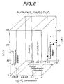
- a phase diagram of the Bi 2 (Sr 2 Ca 1 ) 1-x (La 2 Y 1 ) x Cu y O z system oxide compound is a seven-element system, which is not yet complete at a preliminary stage. Particularly important is control of z for the oxygen deficiency corresponding to a set of composition ratios of x and y. In spite of many scientists' remarkable efforts, it will take some more time to completes it. The inventor has been interested in not only a superconductive phase but also a photoconductivity in a semiconductor phase and an insulator phase in the dark.
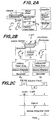
- an electric field pulse E was sustained at a certain value up to E ⁇ 5 KV/cm with 10 msec duration in a repetition rate of 13 Hz.
- Photoexcitation by using a dye laser pulse of 3 nsec in width was synchronized at a suitable time within the time duration of applied electric field pulse (see Fig. 2C).
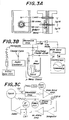
- Static magnetic susceptibility or magnitude of magnetization M can be measured at a weak field up to H ⁇ 500 Oe by using a microwave SQUID at 9 GHz band. Characteristic features of this measurement are separately described (see Figs. 3A, 3B and 3C).
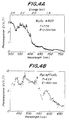
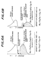
- Fig. 4A is the typical spectra response of pulse photoconductivity Q( ⁇ ,T) of Specimen No. BO3 of Bi 2 O 3
- Fig. 4A is new datum of photoconductivity spectra corresponding to light absorption of Bi 2 O 3 first observed by the inventor throughout the world and should be used as a standard.
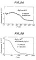
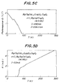
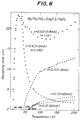
- Fig. 5D exemplified the dark resistivity ⁇ (T) of Specimen No. S182 of superconductor Bi 2 (Sr 2 Ca 1 ) 1 Cu 2 O z as a function of temperature.
- T the photoconductive response Q( ⁇ ,T) displayed in Fig. 5C has a surprisingly well one to one correspondence thereto.
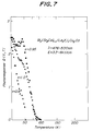
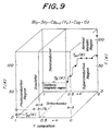
- both superconductive and photoconductive regions have several values of the critical temperatures Tsc and the emergence or step temperatures Tps, respectively.
- the values of Tsc and Tps vary with x. They slightly shift but correspond to each other across their transition regions.
- a specimen of the Bi 2 (Sr 2 Ca 3 ) 1-x (La 2 Y 1 ) x Cu y O z system in the semiconductor or insulator region is usually gray in color.
- a photoconductive spectral response Q( ⁇ ,T) shown in Figs. 4A and 4B suggests that there exists a region similar to Bi 2 O 3 even not necessarily in atomic layers but to some extent within the inside of the specimens of the Bi 2 (Sr 2 Ca 1 ) 1-x (La 2 Y 1 ) x Cu 2 O z system.
- the inventor has found that the critical temperatures 115 K-105 K (high Tc phase) and 85-65 K (low Tc phase) for starting superconductivity expected in the known superconductor well correspond to the temperature for revealing the superconductivity and the temperature for revealing photoresponse in the superconductive conjugate photoconductive substance according to the present invention.
- Fig. 11 is a schematic cross section to exemplify constructed form of a superconductive optoelectronic element according to the present invention.
- the element as a superconductive phototransistor (V G ⁇ 0).
- a photoconductive gate region 2 On the substrate 1, e.g., made of SrTiO 3 , is formed a photoconductive gate region 2.
- the gate region 2 comprises a superconductive-conjugate photoconductive Bi-(SrCa)(LaY)CuO layer of 0.2 ⁇ m-1.0 mm in width and 1-10 ⁇ m in thickness.
- This Bi-(SrCa)(LaY)CuO layer provides special photoconductivity at and below a critical temperature of 105-115 K and 65-85 K of a certain superconductive material consisting of Bi-(SrCa)(LaY)CuO at photoexcitation in the wavelength region of 420-670 nm.
- a source region 3 and a drain region 4 are formed on both sides of the gate region 2 .
- These source region 3 and drain region 4 are composed of a Bi(SrCa)(LaY)CuO superconductive layer showing superconductivity at and below a critical temperature of 105-115 (K) and 65-85 K.
- the source region 3 and the drain region 4 is formed an SiO 2 layer 5 of 1 ⁇ m in thickness with optically transparent and electrically insulating properties, and a NESA (registered Trade Mark) glass layer 6 with bias electrodes is formed thereon.
- a bias source V G Between the bias electrode on the NESA glass layer and the source region 3 is connected a bias source V G and between the source region 3 and the drain region 4 are connected a bias source V SD and an output resistance R.
- the source region and the drain region are particularly made of superconductive material, so that a substantially new superconductive optoelectronic element can be realized without heat dissipation during operation.
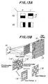
- Fig. 12 is a schematic diagram showing an embodiment of integrating the superconductive optoelectronic elements shown in Fig. 11 in the form of an array.
- the superconductive optoelectronic elements according to the present invention are integrated at high density in the form of one dimensional or two dimensional array, it is possible to materialize a device like a camera by minimizing heat dissipation during operation with appropriate superconductive wirings among various elements as a background. It is also possible to materialize the main portions for signal detection in an optical computer for performing a spatially parallel operation. There is also a possibility of multi-channel operation by selecting the wavelength of an incident light source used.
- Figs. 13A and 13B schematically illustrate an embodiment of optical operation in the projection-correlation optical system of the spatially parallel optical computer [see T. Yatagai: OYO BUTSURI (Applied Physics in Japanese), 57 (1988) p. 1136] with the use of superconductive optoelectronic elements according to the present invention.
- a plurality of optical signals made in parallel from an array-like light source 10 are projected onto an encoded image mask pattern 11.
- the image mask pattern 11 carries encoded image information in a mask fashion.
- a plurality of light beams passed through the encoded image mask pattern 11 are incident in parallel to each element corresponding to a composite mask optical element array 13 via a correlation image screen 12.
- each element of the optical element array 13 is constructed with the superconductive optoelectronic element according to the present invention, it is possible to carry out a parallel optical operation under the condition of minimizing heat dissipation during the operation.
- the embodiment described above represents the three-terminal element as an example, but a two-terminal element also can be realized.
- Such a two-terminal element can hold a position as "superconductive photoconductive or optically controlled Josephson junction device". In this case, it is necessary to appropriately select gate width and incident light amount.
Landscapes
- Engineering & Computer Science (AREA)
- Chemical & Material Sciences (AREA)
- Ceramic Engineering (AREA)
- Manufacturing & Machinery (AREA)
- Materials Engineering (AREA)
- Structural Engineering (AREA)
- Organic Chemistry (AREA)
- Inorganic Compounds Of Heavy Metals (AREA)
- Superconductor Devices And Manufacturing Methods Thereof (AREA)
- Compositions Of Oxide Ceramics (AREA)
- Superconductors And Manufacturing Methods Therefor (AREA)
Claims (3)
- Photoleitfähige Substanz mit der allgemeinen chemischen Formel:
Bi2(Sr2Ca1)1-x(La2Y1)xCu2O z ,
mit 0,4≦x≦1 und z = 9-10,5, wobei die Substanz im Dunkeln ein Isolator oder Halbleiter ist und bei Temperaturen unterhalb 105-115 K oder bei Temperaturen unterhalb 65-85 K unter Photoanregung im Wellenlängenbereich (λ) von 420-670 nm Photoleitfähigkeit aufweist. - Verfahren zur Herstellung einer in Anspruch 1 definierten photoleitfähigen Substanz, mit den Schritten:
primäres Sintern eines Ausgangsmaterials einer Zusammensetzung mit der allgemeinen chemischen Formel:
Bi2(Sr2Ca1)1-x(La2Y1)xCu2O z
mit 0,4≦x≦1 und z = 9-10,5, bei einer Temperatur von 800-840°C über 8-15 Stunden, um eine Festphasenreaktion der Substanz herbeizuführen;
8-15-stündiges Tempern;
sekundäres Sintern bei einer Temperatur von 900-940°C über 8-15 Stunden nach dem Formen unter Druck;
8-15-stündiges Abkühlen; und
Tempern mit einer Abkühlungsgeschwindigkeit von 100-150°C/h. - Supraleitfähiges optoelektronisches Bauelement, das aufweist:
ein isolierendes Substrat (1);
auf dem Substrat ausgebildete Source- und Drain-Elektrodenbereiche (3, 4) aus supraleitfähigem Material, das bei Temperaturen unterhalb einer kritischen Temperatur des Supraleiters supraleitend ist;
einen zwischen den Source- und Drain-Elektrodenbereichen (3, 4) ausgebildeten photoleitfähigen Gate-Bereich (2), der im Dunkeln ein Isolator oder ein Halbleiter ist, aber bei Photoanregung in einem bestimmten optischen Wellenlängenbereich (λ) bei einer Temperatur unterhalb der kritischen Temperatur des für die Source- und Drain-Bereiche verwendeten Supraleiters eine Photoleitfähigkeit Q(λ,T) aufweist; und
eine zwischen die Elektrodenbereiche geschaltete Vorspannungsquelle (VG);
dadurch gekennzeichnet, daß die Elektrodenbereiche aus supraleitfähigem Material mit der allgemeinen chemischen Formel:
Bi2(Sr2Ca1)1-x(La2Y1)xCu2O z
bestehen, mit 0≦x≦0,3 und z = 9-10; und
daß der photoleitfähige Gate-Bereich (2) aus einem in Anspruch 1 definierten photoleitfähigen Material besteht;
wobei ein Strom zwischen den Elektroden in Übereinstimmung mit der Intensität des auf den Gate-Bereich auffallenden Lichts gesteuert werden kann.
Applications Claiming Priority (2)
| Application Number | Priority Date | Filing Date | Title |
|---|---|---|---|
| JP199922/91 | 1991-07-16 | ||
| JP3199922A JPH07109905B2 (ja) | 1991-07-16 | 1991-07-16 | Bi−SrCa(LaY)−Cu−O系酸化物超伝導共役性光伝導物質及びその製造法並びにこれを用いた超伝導オプトエレクトロニクス装置 |
Publications (2)
| Publication Number | Publication Date |
|---|---|
| EP0523937A1 EP0523937A1 (de) | 1993-01-20 |
| EP0523937B1 true EP0523937B1 (de) | 1996-11-27 |
Family
ID=16415835
Family Applications (1)
| Application Number | Title | Priority Date | Filing Date |
|---|---|---|---|
| EP92306397A Expired - Lifetime EP0523937B1 (de) | 1991-07-16 | 1992-07-13 | Photoleitfähige Substanzen vom Typ Bismuth-Strontium-Calcium-Lanthan-Yttrium-Kupfer-Sauerstoff |
Country Status (5)
| Country | Link |
|---|---|
| US (2) | US5445766A (de) |
| EP (1) | EP0523937B1 (de) |
| JP (1) | JPH07109905B2 (de) |
| CA (1) | CA2073955C (de) |
| DE (1) | DE69215447T2 (de) |
Families Citing this family (3)
| Publication number | Priority date | Publication date | Assignee | Title |
|---|---|---|---|---|
| US20010047183A1 (en) * | 2000-04-05 | 2001-11-29 | Salvatore Privitera | Surgical device for the collection of soft tissue |
| US20080146965A1 (en) | 2003-08-11 | 2008-06-19 | Salvatore Privitera | Surgical Device for The Collection of Soft Tissue |
| GB0909967D0 (en) * | 2009-06-10 | 2009-07-22 | Membrane Extraction Tech Ltd | Polyimide membrane |
Family Cites Families (14)
| Publication number | Priority date | Publication date | Assignee | Title |
|---|---|---|---|---|
| FR2612507B1 (fr) * | 1987-03-19 | 1989-05-05 | Comp Generale Electricite | Oxyde de cuivre a valence mixte supraconducteur et son procede de mise en oeuvre |
| US5189011A (en) * | 1987-07-26 | 1993-02-23 | Sumitomo Electric Industries, Ltd. | Superconducting material and method for preparing the same (Sr, γ)x (La, δ)1-x εy Cu1-y O3-z |
| CA1338754C (en) * | 1987-12-28 | 1996-12-03 | Jun Akimitsu | Metal oxide material |
| JPH085713B2 (ja) * | 1988-02-04 | 1996-01-24 | 東京大学長 | Y―Ba―Cu―O系酸化物光伝導性物質及びその製造方法 |
| JPH085714B2 (ja) * | 1988-02-04 | 1996-01-24 | 東京大学長 | La―Cu―O系酸化物光伝導性物質及びその製造方法 |
| US4990487A (en) * | 1988-03-11 | 1991-02-05 | The University Of Tokyo | Superconductive optoelectronic devices |
| JPH06102549B2 (ja) * | 1988-08-12 | 1994-12-14 | 東京大学長 | Ca−Sr−Bi−Cu−O系酸化物超伝導性光伝導物質及びその製造法 |
| JPH06102548B2 (ja) * | 1988-08-12 | 1994-12-14 | 東京大学長 | Ba−Pb−Bi−O系酸化物超伝導性光伝導物質及びその製造法 |
| US5126316A (en) * | 1988-08-24 | 1992-06-30 | E. I. Du Pont De Nemours And Company | Bi2 Sr3-x Yx Cu2 O8+y superconducting metal oxide compositions |
| JPH02153822A (ja) * | 1988-12-02 | 1990-06-13 | Kyocera Corp | 酸化物超電導体組成物 |
| JPH03137020A (ja) * | 1989-10-18 | 1991-06-11 | Toray Ind Inc | 超伝導体 |
| JPH03285823A (ja) * | 1990-03-30 | 1991-12-17 | Toshiba Corp | 酸化物超電導体 |
| JPH065791B2 (ja) * | 1990-05-11 | 1994-01-19 | 東京大学長 | 超伝導性光伝導基本物質Cu2O系材料を用いた超伝導オプトエレクトロニクス装置 |
| JPH065792B2 (ja) * | 1990-08-03 | 1994-01-19 | 東京大学長 | 超伝導性光伝導基本物質Bi▲下2▼0▲下3▼系材料を用いた超伝導オプトエレクトロニクス装置 |
-
1991
- 1991-07-16 JP JP3199922A patent/JPH07109905B2/ja not_active Expired - Lifetime
-
1992
- 1992-07-13 EP EP92306397A patent/EP0523937B1/de not_active Expired - Lifetime
- 1992-07-13 DE DE69215447T patent/DE69215447T2/de not_active Expired - Fee Related
- 1992-07-15 CA CA002073955A patent/CA2073955C/en not_active Expired - Fee Related
- 1992-07-15 US US07/913,431 patent/US5445766A/en not_active Expired - Fee Related
-
1995
- 1995-06-07 US US08/473,905 patent/US5654259A/en not_active Expired - Fee Related
Also Published As
| Publication number | Publication date |
|---|---|
| DE69215447T2 (de) | 1997-04-24 |
| EP0523937A1 (de) | 1993-01-20 |
| US5445766A (en) | 1995-08-29 |
| DE69215447D1 (de) | 1997-01-09 |
| US5654259A (en) | 1997-08-05 |
| JPH06318738A (ja) | 1994-11-15 |
| JPH07109905B2 (ja) | 1995-11-22 |
| CA2073955C (en) | 1999-04-06 |
| CA2073955A1 (en) | 1993-01-17 |
Similar Documents
| Publication | Publication Date | Title |
|---|---|---|
| EP0332448B1 (de) | Supraleitende optoelektronische Einrichtungen | |
| US5445766A (en) | Superconductive conjugate photoconductive substances of the Bi-SrCa(LaY)-Cu-O system, a method for producing the same and superconductive optoelectronic devices using the same | |
| US5554584A (en) | Superconductive photoconductive substance of the Ca-Sr-Bi-Cu-O group system and a method of producing the same | |
| CA1338852C (en) | Superconductive photoconductive-substance of the la-cu-o system and a method for producing the same | |
| EP0354811B1 (de) | Supraleitende photoleitfähige Substanz vom System Ba-Pb-Bi-O und Herstellungsverfahren | |
| Chen et al. | Resistivity and thermoelectric power of Bi2Sr2Ca− xPrxCu2Oy system | |
| EP0456513B1 (de) | Supraleitende, optoelektonische Einrichtung mit Cu20 als photoleitenden Material | |
| US5219831A (en) | Superconductive photoconductive-substance of the La-Cu-O system and a method for producing the same | |
| EP0469922B1 (de) | Supraleitende optoelektronische Vorrichtungen mit der Grundsubstanz Bi203 von supraleitend-konjugierter Photoleitfähigkeit | |
| US5168165A (en) | Superconductive photoconductive-substance of the Y-Ba-Cu-O system and a method for producing the same | |
| US5098868A (en) | Vanadium-based superconducting metallic oxides | |
| CA1338851C (en) | Superconductive photoconductive-substance of the y-ba-cu-o system and a method for producing the same | |
| US5140002A (en) | Photoconductive-substance of the Y-Ba-Cu-O system and a method for producing the same | |
| Masumi | Photoconductivity with anomalies in insulators correlated with high-Tc superconductivity | |
| Er et al. | XANES study on electron doped infinite-layer Sr1− xLaxCuO2 (0≤ x≤ 0.12) and (Sr1− yCay) 0.9 La0. 1CuO2 (0≤ y≤ 0.20) superconductors | |
| Alimardan et al. | Partial substitution Effect of Pb and Mg on the Structural and Electrical Properties of High Temperature (Hg1-xPbxBa2Ca3-yMgyCu4O10+ δ) Superconductor | |
| Huve et al. | Influence of the size of alkaline earth cations on the structural distortion and transport properties of the semiconducting 1212-type cuprates TlBa2− xSrxLnCu2O7 | |
| Narlikar et al. | High-temperature superconducting cuprates: Substitutional and related studies | |
| Raveau et al. | Irradiation Effects in the High-Tc Superconducting Oxides | |
| Fang | Interfacial studies of high temperature superconducting bismuth (2) strontium (2) calcium (n-1) copper (n) oxygen (2n+ 4) and silver |
Legal Events
| Date | Code | Title | Description |
|---|---|---|---|
| PUAI | Public reference made under article 153(3) epc to a published international application that has entered the european phase |
Free format text: ORIGINAL CODE: 0009012 |
|
| AK | Designated contracting states |
Kind code of ref document: A1 Designated state(s): BE CH DE FR GB IT LI NL |
|
| 17P | Request for examination filed |
Effective date: 19930303 |
|
| 17Q | First examination report despatched |
Effective date: 19941007 |
|
| GRAG | Despatch of communication of intention to grant |
Free format text: ORIGINAL CODE: EPIDOS AGRA |
|
| GRAH | Despatch of communication of intention to grant a patent |
Free format text: ORIGINAL CODE: EPIDOS IGRA |
|
| GRAH | Despatch of communication of intention to grant a patent |
Free format text: ORIGINAL CODE: EPIDOS IGRA |
|
| GRAA | (expected) grant |
Free format text: ORIGINAL CODE: 0009210 |
|
| AK | Designated contracting states |
Kind code of ref document: B1 Designated state(s): BE CH DE FR GB IT LI NL |
|
| ITF | It: translation for a ep patent filed | ||
| REG | Reference to a national code |
Ref country code: CH Ref legal event code: NV Representative=s name: PATENTANWAELTE SCHAAD, BALASS, MENZL & PARTNER AG |
|
| REF | Corresponds to: |
Ref document number: 69215447 Country of ref document: DE Date of ref document: 19970109 |
|
| ET | Fr: translation filed | ||
| PLBE | No opposition filed within time limit |
Free format text: ORIGINAL CODE: 0009261 |
|
| STAA | Information on the status of an ep patent application or granted ep patent |
Free format text: STATUS: NO OPPOSITION FILED WITHIN TIME LIMIT |
|
| 26N | No opposition filed | ||
| K2C3 | Correction of patent specification (complete document) published |
Effective date: 19961127 |
|
| PGFP | Annual fee paid to national office [announced via postgrant information from national office to epo] |
Ref country code: DE Payment date: 20010709 Year of fee payment: 10 |
|
| PGFP | Annual fee paid to national office [announced via postgrant information from national office to epo] |
Ref country code: GB Payment date: 20010711 Year of fee payment: 10 |
|
| PGFP | Annual fee paid to national office [announced via postgrant information from national office to epo] |
Ref country code: FR Payment date: 20010712 Year of fee payment: 10 |
|
| PGFP | Annual fee paid to national office [announced via postgrant information from national office to epo] |
Ref country code: CH Payment date: 20010713 Year of fee payment: 10 |
|
| PGFP | Annual fee paid to national office [announced via postgrant information from national office to epo] |
Ref country code: NL Payment date: 20010730 Year of fee payment: 10 |
|
| PGFP | Annual fee paid to national office [announced via postgrant information from national office to epo] |
Ref country code: BE Payment date: 20010918 Year of fee payment: 10 |
|
| REG | Reference to a national code |
Ref country code: GB Ref legal event code: IF02 |
|
| PG25 | Lapsed in a contracting state [announced via postgrant information from national office to epo] |
Ref country code: GB Free format text: LAPSE BECAUSE OF NON-PAYMENT OF DUE FEES Effective date: 20020713 |
|
| PG25 | Lapsed in a contracting state [announced via postgrant information from national office to epo] |
Ref country code: LI Free format text: LAPSE BECAUSE OF NON-PAYMENT OF DUE FEES Effective date: 20020731 Ref country code: CH Free format text: LAPSE BECAUSE OF NON-PAYMENT OF DUE FEES Effective date: 20020731 Ref country code: BE Free format text: LAPSE BECAUSE OF NON-PAYMENT OF DUE FEES Effective date: 20020731 |
|
| BERE | Be: lapsed |
Owner name: THE *UNIVERSITY OF TOKYO Effective date: 20020731 |
|
| PG25 | Lapsed in a contracting state [announced via postgrant information from national office to epo] |
Ref country code: NL Free format text: LAPSE BECAUSE OF NON-PAYMENT OF DUE FEES Effective date: 20030201 Ref country code: DE Free format text: LAPSE BECAUSE OF NON-PAYMENT OF DUE FEES Effective date: 20030201 |
|
| GBPC | Gb: european patent ceased through non-payment of renewal fee |
Effective date: 20020713 |
|
| REG | Reference to a national code |
Ref country code: CH Ref legal event code: PL |
|
| PG25 | Lapsed in a contracting state [announced via postgrant information from national office to epo] |
Ref country code: FR Free format text: LAPSE BECAUSE OF NON-PAYMENT OF DUE FEES Effective date: 20030331 |
|
| NLV4 | Nl: lapsed or anulled due to non-payment of the annual fee |
Effective date: 20030201 |
|
| REG | Reference to a national code |
Ref country code: FR Ref legal event code: ST |
|
| PG25 | Lapsed in a contracting state [announced via postgrant information from national office to epo] |
Ref country code: IT Free format text: LAPSE BECAUSE OF NON-PAYMENT OF DUE FEES;WARNING: LAPSES OF ITALIAN PATENTS WITH EFFECTIVE DATE BEFORE 2007 MAY HAVE OCCURRED AT ANY TIME BEFORE 2007. THE CORRECT EFFECTIVE DATE MAY BE DIFFERENT FROM THE ONE RECORDED. Effective date: 20050713 |