EP0519441A2 - Schmierausgleichschaltung für einen Festkörper-Bildaufnehmer - Google Patents
Schmierausgleichschaltung für einen Festkörper-Bildaufnehmer Download PDFInfo
- Publication number
- EP0519441A2 EP0519441A2 EP92110257A EP92110257A EP0519441A2 EP 0519441 A2 EP0519441 A2 EP 0519441A2 EP 92110257 A EP92110257 A EP 92110257A EP 92110257 A EP92110257 A EP 92110257A EP 0519441 A2 EP0519441 A2 EP 0519441A2
- Authority
- EP
- European Patent Office
- Prior art keywords
- smear
- memory
- solid state
- video signal
- compensation circuit
- Prior art date
- Legal status (The legal status is an assumption and is not a legal conclusion. Google has not performed a legal analysis and makes no representation as to the accuracy of the status listed.)
- Granted
Links
Images

Classifications
-
- H—ELECTRICITY
- H04—ELECTRIC COMMUNICATION TECHNIQUE
- H04N—PICTORIAL COMMUNICATION, e.g. TELEVISION
- H04N25/00—Circuitry of solid-state image sensors [SSIS]; Control thereof
- H04N25/60—Noise processing, e.g. detecting, correcting, reducing or removing noise
-
- H—ELECTRICITY
- H04—ELECTRIC COMMUNICATION TECHNIQUE
- H04N—PICTORIAL COMMUNICATION, e.g. TELEVISION
- H04N25/00—Circuitry of solid-state image sensors [SSIS]; Control thereof
- H04N25/60—Noise processing, e.g. detecting, correcting, reducing or removing noise
- H04N25/62—Detection or reduction of noise due to excess charges produced by the exposure, e.g. smear, blooming, ghost image, crosstalk or leakage between pixels
- H04N25/625—Detection or reduction of noise due to excess charges produced by the exposure, e.g. smear, blooming, ghost image, crosstalk or leakage between pixels for the control of smear
-
- H—ELECTRICITY
- H04—ELECTRIC COMMUNICATION TECHNIQUE
- H04N—PICTORIAL COMMUNICATION, e.g. TELEVISION
- H04N25/00—Circuitry of solid-state image sensors [SSIS]; Control thereof
- H04N25/70—SSIS architectures; Circuits associated therewith
- H04N25/71—Charge-coupled device [CCD] sensors; Charge-transfer registers specially adapted for CCD sensors
- H04N25/73—Charge-coupled device [CCD] sensors; Charge-transfer registers specially adapted for CCD sensors using interline transfer [IT]
Definitions
- the present invention generally relates to smear compensation circuits for eliminating a smear component which is contained in and peculiar to an output of a solid state imager and, more particularly, to a smear compensation circuit for compensating for a smear of an output from camera apparatus such as a video camera using a solid state image pickup device or the like.
- a color aliasing signal known as a smear
- the smear component occurs when a light is directly introduced into a vertical transfer section or when charges produced within a semiconductor substrate are expanded by the diffusion and mixed into the vertical transfer section.
- the smear component tends to occur particularly when the cameraman takes a picture of an object having high brightness, which causes the quality of a reproduced image to be deteriorated.
- smear compensation circuits for compensating for the smear component inherent in the solid state image pickup devices
- a smear compensation circuit in which a smear component in the vertical blanking period is written in a memory and a smear component read out from the memory during the video period is subtracted from a video signal to thereby compensate for the smear component because only the smear component exists during the vertical blanking period and the smear component is superposed on the video signal during the video period.
- Japanese Laid-Open Patent Publication No. 63-173474 describes this conventional smear compensation circuit.
- the conventional smear compensation circuit which uses a memory of a limited bit capacity in order to reduce the capacity of the memory, could not fulfil both a quantization noise (data length per bit) and a dynamic range (maximum compensation range). That is, if the former is satisfied, then a compensation signal is clipped when there are too much smear component and the smear components cannot be fully compensated for. If the latter is satisfied, then a vertical distortion appears due to a quantization noise, which causes the quality of image to be deteriorated.
- a smear compensation circuit for a solid state imager is comprised of an analog-to-digital converter for converting an analog video signal supplied thereto from an output of a solid state imager into a digital video signal, a peak detecting circuit coupled to an output of the analog-to-digital converter for detecting a peak value of the digital video signal in a vertical blanking period, a memory for storing therein write data in which the level of the digital video signal is adjusted by a first level adjusting circuit coupled to the output of the analog-to-digital converter on the basis of an output from the peak detecting circuit, a second level adjusting circuit for adjusting a level of read-out data read out from the memory, and a subtracting circuit for subtracting from the digital video signal a value in which the level of the read-out data read out from the memory is level-adjusted by the second level adjusting circuit during a video period of the digital video signal.
- a peak value of the digital video signal in the vertical blanking period is detected and a gain of smear data written in a memory is adjusted in response to the detected peak value, whereby the data is stored in the memory having a restricted memory capacity. Further, when the data is read out from the memory, the gain of the read-out data is adjusted in an opposite manner to thereby obtain a smear component of the original level. Then, this smear component is subtracted from the video signal to thereby obtain a video signal whose smear component is eliminated. Consequently, the memory capacity can be reduced without deteriorating the quality of a reproduced image based on an output of a solid state image pickup device.
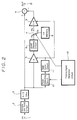
- FIG. 2 of the accompanying drawings shows in block form a smear compensation circuit according to a first embodiment of the present invention.
- an imager output from a solid state imager device e.g., CCD (charge coupled device) image sensor (not shown) is supplied to an input terminal 1.
- a video signal of this imager output is sampled by a sample and hold circuit 2 and then converted into a digital video signal by an analog-to-digital (A/D) converter 3.
- A/D analog-to-digital
- the digital video signal from the A/D converter 3 is supplied to a subtracting circuit 4 as a subtracted input and also supplied through a gain adjusting circuit 5 and a level clipping circuit 6 to a first fixed contact 7a of a change-over circuit 7.
- a 1H (H represents a horizontal scanning period) memory 8 is coupled to a movable contact 7c of the change-over switch 7 so that, when the change-over switch 7 connects the movable contact 7c to the first fixed contact 7a, smear data is written in the 1H memory 8. Also, when the change-over switch 7 connects the movable contact 7c to a second fixed contact 7b, smear data is read out from the 1H memory 8.
- the smear data read out from the 1H memory 8 is supplied through a gain adjusting circuit 9 to the subtracting circuit 4 as a subtracting input.
- the gain adjusting circuits 5 and 9 are adapted to adjust gains of the data written in the 1H memory 8 and the data read out from the 1H memory 8 in a complementary fashion. That is, assuming that A is the gain of the gain adjusting circuit 5, then the gain of the gain adjusting circuit 9 becomes 1/A.
- the digital video signal is also supplied to a peak detecting circuit 10.
- the peak detecting circuit 10 is adapted to detect a peak value of a smear component existing in a vertical blanking period VBLK.
- a peak value information from the peak detecting circuit 10 is supplied to a gain converting circuit 11.
- the gain converting circuit 11 operates to set the gains A and 1/A of the gain adjusting circuits 5 and 9 on the basis of the peak value of the smear component.
- a timing at which the peak detecting circuit 10 detects the peak value is determined by a timing signal generated from a timing generator circuit 12.
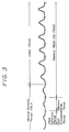
- a duration of this detection timing must be set to 1H period of at least 3H before the vertical blanking period VBLK of the video signal is ended because an extra period of 2H is needed in order to write data of 1H period in the 1H memory 8 and to read out the data of 1H period from the 1H memory 8 as shown in a timing chart forming FIG. 2.
- the change-over switch 7 is changed-over in response to a switching control signal generated from the timing generator circuit 12.
- the writing of data in the 1H memory 8 is started from a timing of 2 H before the end of the vertical blanking period VBLK, which requires the change-over switch 7 to connect the movable contact 7c to the first fixed contact 7a at least on or before such timing point.
- the change-over switch 7 connects the movable contact 7c to the second fixed contact 7b before 1H of the end of the vertical blanking period VBLK, whereby the smear data is read out from the 1H memory 8 until the start of the video period.
- the peak value of the smear component is detected during 1H period of 3H before the end of the vertical blanking period VBLK. Since it is to be noted that the smear component can constantly present a substantially constant peak value, the peak value of the smear component can be detected as substantially the same value during any period of the vertical blanking period.
- the gain converting circuit 11 sets the gain A of the gain adjusting circuit 5 on the basis of the peal value of this smear component.
- the smear data whose gain is adjusted by the gain A is clipped by the clipping circuit 6 and then written in the 1H memory 8.
- the level clipping circuit 6 is provided in order to eliminate a noise component which causes the 1H memory 8 to overflow in memory capacity because there is the possibility that the level of the smear component will change during the peak detection period and during the memory writing period due to a random noise although the smear component in the vertical blanking period is the same in level inherently.
- the change-over switch 7 connects the movable contact 7c to the second fixed contact 7b to allow the smear data from being read out from the 1H memory 8. Then, the smear data thus read out is gain-adjusted in a complementary fashion by the gain 1/A which is the reciprocal number of the gain A in the writing and thereby is returned to the gain provided when the peak value is detected, whereafter it is subtracted from the video signal on which the smear component is superimposed. As a consequence, only a video signal whose smear component is eliminated can be delivered from an output terminal 13 led out from the subtracting circuit 4.
- the peak value of the smear component to be stored in the 1H memory is detected, and the smear component is gain-adjusted so as to fall within the dynamic range of the 1H memory 8 in response to the detected peak value.
- the thus gain-adjusted smear component is written in the 1H memory 8 and read out from the 1H memory 8.
- the thus read-out smear component is gain-adjusted in a complementary fashion by the gain in the writing and thereby is returned to the original level, whereafter the smear component is subtracted from the video signal to provide the video signal whose smear component is eliminated. Therefore, the memory capacity of the 1H memory 8 can be reduced without deteriorating the quality of the reproduced image based on the output from the solid state imager.
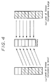
- FIG. 4 of the accompanying drawings is a diagram used to explain operation of the present invention in which a block input is 8 bits and a memory capacity is 6 bits.
- (a) in FIG. 4 shows the case such that the level of the smear component is small, while (b) in FIG. 4 shows the case such that the level of the smear component is large.
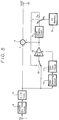
- FIG. 5 of the accompanying drawings shows a block diagram of a second embodiment of the smear compensation circuit according to the present invention.
- like parts corresponding to those of FIG. 2 are marked with the same references and therefore need not be described in detail.
- a gain adjusting circuit 14 operates to adjust the gains of the smear components both when the smear component is written in and read out from the 1H memory.
- a change-over switch 15 is adapted to switch the writing and reading in the 1H memory 8.
- the gain converting circuit 11 operates to switch the gain of the gain adjusting circuit 14 such that the gain of the gain adjusting circuit 14 become A when the smear data is written in the 1H memory 8 and 1/A when the smear data is read out from the 1H memory 8.
- the gain adjusting circuits 5, 9 and 14 might be generally formed of a multiplier.
- the multiplier is generally large in circuit scale and becomes complex in circuit configuration.
- a x 2 n selector i.e., a bit shifting circuit is employed in order to simplify the circuit configuration.
- the peal value of the digital video signal in the vertical blanking period is detected and the gain of data stored in the memory is adjusted in response to the detected peak value so that the data is stored in the restricted memory capacity. Further, when the data is read out from the memory, the gain is adjusted in a complementary fashion to provide the smear component of the original level and this smear component is subtracted from the video signal.
- the memory capacity can be reduced without deteriorating the quality of the reproduced picture based on the output of the solid state imager.
Landscapes
- Engineering & Computer Science (AREA)
- Multimedia (AREA)
- Signal Processing (AREA)
- Transforming Light Signals Into Electric Signals (AREA)
Applications Claiming Priority (2)
| Application Number | Priority Date | Filing Date | Title |
|---|---|---|---|
| JP3177175A JPH04373277A (ja) | 1991-06-21 | 1991-06-21 | スメア補正回路 |
| JP177175/91 | 1991-06-21 |
Publications (3)
| Publication Number | Publication Date |
|---|---|
| EP0519441A2 true EP0519441A2 (de) | 1992-12-23 |
| EP0519441A3 EP0519441A3 (en) | 1993-08-25 |
| EP0519441B1 EP0519441B1 (de) | 1997-03-05 |
Family
ID=16026496
Family Applications (1)
| Application Number | Title | Priority Date | Filing Date |
|---|---|---|---|
| EP92110257A Expired - Lifetime EP0519441B1 (de) | 1991-06-21 | 1992-06-17 | Schmierausgleichschaltung für einen Festkörper-Bildaufnehmer |
Country Status (5)
| Country | Link |
|---|---|
| US (1) | US5485205A (de) |
| EP (1) | EP0519441B1 (de) |
| JP (1) | JPH04373277A (de) |
| KR (1) | KR930020969A (de) |
| DE (1) | DE69217731T2 (de) |
Families Citing this family (6)
| Publication number | Priority date | Publication date | Assignee | Title |
|---|---|---|---|---|
| US6049330A (en) * | 1997-08-28 | 2000-04-11 | Oak Technology, Inc. | Method and apparatus for optimizing storage of compressed images in memory |
| US6166831A (en) * | 1997-12-15 | 2000-12-26 | Analog Devices, Inc. | Spatially offset, row interpolated image sensor |
| US6914627B1 (en) * | 1998-05-27 | 2005-07-05 | Omnivision Technologies, Inc. | Method and apparatus for digital column fixed pattern noise canceling for a CMOS image sensor |
| US6809763B1 (en) * | 1999-08-02 | 2004-10-26 | Olympus Optical Co., Ltd. | Image pickup apparatus and method of correcting deteriorated pixel signal thereof |
| JP2005094678A (ja) * | 2003-09-19 | 2005-04-07 | Sanyo Electric Co Ltd | ビデオ信号処理装置及びテレビジョン受像装置 |
| JP4742652B2 (ja) * | 2005-04-14 | 2011-08-10 | 富士フイルム株式会社 | 撮像装置 |
Family Cites Families (20)
| Publication number | Priority date | Publication date | Assignee | Title |
|---|---|---|---|---|
| US4010319A (en) * | 1975-11-20 | 1977-03-01 | Rca Corporation | Smear reduction in ccd imagers |
| JPS57133776A (en) * | 1981-02-13 | 1982-08-18 | Nec Corp | Solid-state image pickup device |
| JPS5814682A (ja) * | 1981-07-20 | 1983-01-27 | Sony Corp | 固体撮像装置 |
| JPS5827472A (ja) * | 1981-08-10 | 1983-02-18 | Sony Corp | 固体撮像装置の制御装置 |
| JPS58156272A (ja) * | 1982-03-12 | 1983-09-17 | Sony Corp | スミア補正回路 |
| JPS58195372A (ja) * | 1982-05-10 | 1983-11-14 | Nec Corp | 撮像装置 |
| JPS59275A (ja) * | 1982-06-25 | 1984-01-05 | Sony Corp | 固体撮像素子のスミア補正回路 |
| JPS59211385A (ja) * | 1983-05-16 | 1984-11-30 | Sony Corp | スミア補正回路 |
| JPS60112376A (ja) * | 1983-11-22 | 1985-06-18 | Sanyo Electric Co Ltd | 撮像装置 |
| GB2151430A (en) * | 1983-11-30 | 1985-07-17 | Hitachi Ltd | Solid-state imaging system with smear suppression circuits |
| GB8518067D0 (en) * | 1985-07-17 | 1985-08-21 | Gen Electric Co Plc | Image sensors |
| JP2579930B2 (ja) * | 1987-03-17 | 1997-02-12 | 株式会社東芝 | 複合信号分離回路 |
| JPH085210B2 (ja) * | 1987-06-19 | 1996-01-24 | 富士写真フイルム株式会社 | 光ビ−ム走査記録装置およびその制御方法 |
| JPH01106677A (ja) * | 1987-10-20 | 1989-04-24 | Sony Corp | 電荷転送素子の出力回路 |
| GB8826463D0 (en) * | 1988-11-11 | 1988-12-14 | Rca Licensing Corp | Technique for actv side-panel noise reduction |
| JP2643422B2 (ja) * | 1989-03-14 | 1997-08-20 | 松下電器産業株式会社 | 相関演算装置 |
| US5016107A (en) * | 1989-05-09 | 1991-05-14 | Eastman Kodak Company | Electronic still camera utilizing image compression and digital storage |
| JPH02301270A (ja) * | 1989-05-15 | 1990-12-13 | Sanyo Electric Co Ltd | 固体撮像素子のスミア除去回路 |
| US5005082A (en) * | 1989-10-03 | 1991-04-02 | General Electric Company | Video signal compander adaptively responsive to predictions of the video signal processed |
| US5321522A (en) * | 1993-07-19 | 1994-06-14 | Xerox Corporation | ADCT compression with minimum compression ratio |
-
1991
- 1991-06-21 JP JP3177175A patent/JPH04373277A/ja active Pending
-
1992
- 1992-06-16 KR KR1019920010388A patent/KR930020969A/ko not_active Withdrawn
- 1992-06-17 DE DE69217731T patent/DE69217731T2/de not_active Expired - Fee Related
- 1992-06-17 EP EP92110257A patent/EP0519441B1/de not_active Expired - Lifetime
-
1994
- 1994-05-31 US US08/250,949 patent/US5485205A/en not_active Expired - Fee Related
Also Published As
| Publication number | Publication date |
|---|---|
| DE69217731D1 (de) | 1997-04-10 |
| US5485205A (en) | 1996-01-16 |
| EP0519441B1 (de) | 1997-03-05 |
| KR930020969A (ko) | 1993-10-20 |
| JPH04373277A (ja) | 1992-12-25 |
| EP0519441A3 (en) | 1993-08-25 |
| DE69217731T2 (de) | 1997-09-25 |
Similar Documents
| Publication | Publication Date | Title |
|---|---|---|
| US8982252B2 (en) | Image sensing device using a photoelectric converter and a control method therefor | |
| US5134487A (en) | Using common circuitry for different signals | |
| KR100411207B1 (ko) | 디지탈카메라 | |
| US4581651A (en) | Smear reduction in solid state image pickup device camera | |
| US4910598A (en) | Solid state television camera with circuit for cancelling noise due to crystal defects | |
| US20030133035A1 (en) | Image pickup apparatus and method for broadening apparent dynamic range of video signal | |
| US20010055428A1 (en) | Image signal processor with adaptive noise reduction and an image signal processing method therefor | |
| JPH0318393B2 (de) | ||
| US5140424A (en) | Image signal processing apparatus with noise reduction | |
| US4600946A (en) | Adaptive defect correction for solid-state imagers | |
| EP1091572B1 (de) | Bildaufnahmevorrichtung mit einer Funktion zur Regelung der einfallenden Lichtmenge | |
| US5576762A (en) | Solid-state image pickup device | |
| EP0519441B1 (de) | Schmierausgleichschaltung für einen Festkörper-Bildaufnehmer | |
| JP2001245213A (ja) | 撮像装置 | |
| US4547807A (en) | CCD Imager | |
| US6700608B1 (en) | Image pickup apparatus | |
| US5926216A (en) | Image sensing apparatus | |
| EP0753961B1 (de) | Dieselbe Hardware für Aufnahme und Wiedergabe benutzende Bildverarbeitungsvorrichtung | |
| US5323238A (en) | Image signal processing apparatus having improved storage control in accordance with an image signal level | |
| JP2007036457A (ja) | 撮像装置 | |
| JP3744160B2 (ja) | 映像信号処理方法及び映像信号処理装置 | |
| JP2970092B2 (ja) | ビデオカメラ | |
| US8330842B2 (en) | Amplifier control device and recording non-transitory medium | |
| JP2755514B2 (ja) | Ccd固体撮像装置 | |
| JP2000050148A (ja) | テレビジョンカメラ装置 |
Legal Events
| Date | Code | Title | Description |
|---|---|---|---|
| PUAI | Public reference made under article 153(3) epc to a published international application that has entered the european phase |
Free format text: ORIGINAL CODE: 0009012 |
|
| AK | Designated contracting states |
Kind code of ref document: A2 Designated state(s): DE FR GB |
|
| PUAL | Search report despatched |
Free format text: ORIGINAL CODE: 0009013 |
|
| AK | Designated contracting states |
Kind code of ref document: A3 Designated state(s): DE FR GB |
|
| 17P | Request for examination filed |
Effective date: 19940125 |
|
| 17Q | First examination report despatched |
Effective date: 19951219 |
|
| GRAG | Despatch of communication of intention to grant |
Free format text: ORIGINAL CODE: EPIDOS AGRA |
|
| GRAH | Despatch of communication of intention to grant a patent |
Free format text: ORIGINAL CODE: EPIDOS IGRA |
|
| GRAH | Despatch of communication of intention to grant a patent |
Free format text: ORIGINAL CODE: EPIDOS IGRA |
|
| GRAA | (expected) grant |
Free format text: ORIGINAL CODE: 0009210 |
|
| AK | Designated contracting states |
Kind code of ref document: B1 Designated state(s): DE FR GB |
|
| REF | Corresponds to: |
Ref document number: 69217731 Country of ref document: DE Date of ref document: 19970410 |
|
| ET | Fr: translation filed | ||
| PLBE | No opposition filed within time limit |
Free format text: ORIGINAL CODE: 0009261 |
|
| STAA | Information on the status of an ep patent application or granted ep patent |
Free format text: STATUS: NO OPPOSITION FILED WITHIN TIME LIMIT |
|
| 26N | No opposition filed | ||
| PGFP | Annual fee paid to national office [announced via postgrant information from national office to epo] |
Ref country code: FR Payment date: 20010611 Year of fee payment: 10 Ref country code: DE Payment date: 20010611 Year of fee payment: 10 |
|
| PGFP | Annual fee paid to national office [announced via postgrant information from national office to epo] |
Ref country code: GB Payment date: 20010613 Year of fee payment: 10 |
|
| REG | Reference to a national code |
Ref country code: GB Ref legal event code: IF02 |
|
| PG25 | Lapsed in a contracting state [announced via postgrant information from national office to epo] |
Ref country code: GB Free format text: LAPSE BECAUSE OF NON-PAYMENT OF DUE FEES Effective date: 20020617 |
|
| PG25 | Lapsed in a contracting state [announced via postgrant information from national office to epo] |
Ref country code: DE Free format text: LAPSE BECAUSE OF NON-PAYMENT OF DUE FEES Effective date: 20030101 |
|
| GBPC | Gb: european patent ceased through non-payment of renewal fee |
Effective date: 20020617 |
|
| PG25 | Lapsed in a contracting state [announced via postgrant information from national office to epo] |
Ref country code: FR Free format text: LAPSE BECAUSE OF NON-PAYMENT OF DUE FEES Effective date: 20030228 |
|
| REG | Reference to a national code |
Ref country code: FR Ref legal event code: ST |