EP0518686B1 - Solid state image pick-up device - Google Patents
Solid state image pick-up device Download PDFInfo
- Publication number
- EP0518686B1 EP0518686B1 EP92305420A EP92305420A EP0518686B1 EP 0518686 B1 EP0518686 B1 EP 0518686B1 EP 92305420 A EP92305420 A EP 92305420A EP 92305420 A EP92305420 A EP 92305420A EP 0518686 B1 EP0518686 B1 EP 0518686B1
- Authority
- EP
- European Patent Office
- Prior art keywords
- shielding film
- image pick
- state image
- optical black
- solid
- Prior art date
- Legal status (The legal status is an assumption and is not a legal conclusion. Google has not performed a legal analysis and makes no representation as to the accuracy of the status listed.)
- Expired - Lifetime
Links
- 239000007787 solid Substances 0.000 title 1
- 230000003287 optical effect Effects 0.000 claims description 30
- 239000000758 substrate Substances 0.000 claims description 14
- 239000004065 semiconductor Substances 0.000 claims description 3
- 238000009413 insulation Methods 0.000 description 7
- VYPSYNLAJGMNEJ-UHFFFAOYSA-N Silicium dioxide Chemical compound O=[Si]=O VYPSYNLAJGMNEJ-UHFFFAOYSA-N 0.000 description 6
- 229910052814 silicon oxide Inorganic materials 0.000 description 6
- 230000001681 protective effect Effects 0.000 description 5
- 229910000789 Aluminium-silicon alloy Inorganic materials 0.000 description 3
- 230000015572 biosynthetic process Effects 0.000 description 3
- 238000010438 heat treatment Methods 0.000 description 3
- 238000005259 measurement Methods 0.000 description 3
- 229910021420 polycrystalline silicon Inorganic materials 0.000 description 3
- 229920005591 polysilicon Polymers 0.000 description 3
- 108010010803 Gelatin Proteins 0.000 description 2
- XUIMIQQOPSSXEZ-UHFFFAOYSA-N Silicon Chemical compound [Si] XUIMIQQOPSSXEZ-UHFFFAOYSA-N 0.000 description 2
- 238000000137 annealing Methods 0.000 description 2
- 229920000159 gelatin Polymers 0.000 description 2
- 239000008273 gelatin Substances 0.000 description 2
- 235000019322 gelatine Nutrition 0.000 description 2
- 235000011852 gelatine desserts Nutrition 0.000 description 2
- 230000012447 hatching Effects 0.000 description 2
- 239000000463 material Substances 0.000 description 2
- 238000000034 method Methods 0.000 description 2
- 230000000452 restraining effect Effects 0.000 description 2
- 229910052710 silicon Inorganic materials 0.000 description 2
- 239000010703 silicon Substances 0.000 description 2
- 239000005018 casein Substances 0.000 description 1
- BECPQYXYKAMYBN-UHFFFAOYSA-N casein, tech. Chemical compound NCCCCC(C(O)=O)N=C(O)C(CC(O)=O)N=C(O)C(CCC(O)=N)N=C(O)C(CC(C)C)N=C(O)C(CCC(O)=O)N=C(O)C(CC(O)=O)N=C(O)C(CCC(O)=O)N=C(O)C(C(C)O)N=C(O)C(CCC(O)=N)N=C(O)C(CCC(O)=N)N=C(O)C(CCC(O)=N)N=C(O)C(CCC(O)=O)N=C(O)C(CCC(O)=O)N=C(O)C(COP(O)(O)=O)N=C(O)C(CCC(O)=N)N=C(O)C(N)CC1=CC=CC=C1 BECPQYXYKAMYBN-UHFFFAOYSA-N 0.000 description 1
- 235000021240 caseins Nutrition 0.000 description 1
- 239000003086 colorant Substances 0.000 description 1
- 239000013078 crystal Substances 0.000 description 1
- 230000008021 deposition Effects 0.000 description 1
- 238000004043 dyeing Methods 0.000 description 1
- 230000002708 enhancing effect Effects 0.000 description 1
- 238000000059 patterning Methods 0.000 description 1
- 239000000049 pigment Substances 0.000 description 1
Images



Classifications
-
- H—ELECTRICITY
- H10—SEMICONDUCTOR DEVICES; ELECTRIC SOLID-STATE DEVICES NOT OTHERWISE PROVIDED FOR
- H10F—INORGANIC SEMICONDUCTOR DEVICES SENSITIVE TO INFRARED RADIATION, LIGHT, ELECTROMAGNETIC RADIATION OF SHORTER WAVELENGTH OR CORPUSCULAR RADIATION
- H10F77/00—Constructional details of devices covered by this subclass
- H10F77/30—Coatings
- H10F77/306—Coatings for devices having potential barriers
- H10F77/331—Coatings for devices having potential barriers for filtering or shielding light, e.g. multicolour filters for photodetectors
-
- H—ELECTRICITY
- H10—SEMICONDUCTOR DEVICES; ELECTRIC SOLID-STATE DEVICES NOT OTHERWISE PROVIDED FOR
- H10F—INORGANIC SEMICONDUCTOR DEVICES SENSITIVE TO INFRARED RADIATION, LIGHT, ELECTROMAGNETIC RADIATION OF SHORTER WAVELENGTH OR CORPUSCULAR RADIATION
- H10F39/00—Integrated devices, or assemblies of multiple devices, comprising at least one element covered by group H10F30/00, e.g. radiation detectors comprising photodiode arrays
- H10F39/10—Integrated devices
- H10F39/12—Image sensors
- H10F39/15—Charge-coupled device [CCD] image sensors
- H10F39/151—Geometry or disposition of pixel elements, address lines or gate electrodes
- H10F39/1515—Optical shielding
-
- H—ELECTRICITY
- H10—SEMICONDUCTOR DEVICES; ELECTRIC SOLID-STATE DEVICES NOT OTHERWISE PROVIDED FOR
- H10F—INORGANIC SEMICONDUCTOR DEVICES SENSITIVE TO INFRARED RADIATION, LIGHT, ELECTROMAGNETIC RADIATION OF SHORTER WAVELENGTH OR CORPUSCULAR RADIATION
- H10F77/00—Constructional details of devices covered by this subclass
- H10F77/30—Coatings
- H10F77/306—Coatings for devices having potential barriers
- H10F77/331—Coatings for devices having potential barriers for filtering or shielding light, e.g. multicolour filters for photodetectors
- H10F77/334—Coatings for devices having potential barriers for filtering or shielding light, e.g. multicolour filters for photodetectors for shielding light, e.g. light blocking layers or cold shields for infrared detectors
Definitions
- the present invention relates generally to a solid-state image pick-up element employing, for example, CCDs (charge coupled devices), and more particularly to a solid-state image pick-up element capable of compensating for changes in characteristics with temperature.
- CCDs charge coupled devices
- Fig. 1 schematically depicts a conventional solid-state image pick-up element of the interline transfer type in which CCDs are used as light receiving units.
- This element is provided with a photoelectric transfer region 102 and an optical black region 103, both of which are formed on a substrate 100.
- a large number of light receiving units 101 are horizontally and vertically regularly arrayed on both the photoelectric transfer region 102 and the optical black region 103.
- the light receiving units 101 of the optical black region 103 are covered with a shielding film (shown by hatching) made of, for example, Al, AlSi or the like.
- the photoelectric transfer region 102 is provided for performing image pick-up whereas the optical black region 103 is provided for compensating signals detected by the photoelectric transfer region 102 for changes with temperature.
- each of the vertical CCD registers 104 is interposed between two adjoining vertical rows of the light receiving units 101 or is formed on the left-hand side of the leftmost vertical row of the light receiving units 101, as viewed in Fig. 1.
- the vertical CCD registers 104 read and transfer signal charges generated in the light receiving units 101.
- the shielding film is made comparatively thin, for example about 1 ⁇ m thick, thereby preventing the generation of pin holes or the lowering in processability, which may be caused if the shielding film is made thick.
- heat treatment such as, for example, H 2 annealing is performed for the purpose of enhancing the quality of the substrate.
- This kind of heat treatment occasionally makes crystals grow upon deposition thereof, thereby producing cracks in the shielding film. Such cracks allow light, though it is slight, to enter the light receiving units 101 of the optical black region 103, thus causing light leakage.
- a silicon oxide insulation film 106 is interposed between the substrate 100 and the shielding film 105, and the upper surface thereof has undulations, for example, across a height of about 1 ⁇ m at regions A, as shown in Fig. 2.
- the presence of such undulations lower the covering state of the shielding film 105, thereby occasionally causing light leakage at the regions A. If the light leakage occurs at the optical black region 103, the dark current value varies and correct temperature compensation cannot be performed.
- JP-A-58-209160 describes a solid-state image pick-up element in which the light-receiving section of a photo-diode is shielded by a first shielding film of Al and a superposed second film comprising a filter pattern.
- a solid-state image pick-up device comprising an array of photoelectric elements formed on a semiconductor substrate, transfer means for effecting transfer of photoelectrically generated charges in a transfer region of the array so as to read out image-defining electrical signals, said transfer means including charge transfer control electrodes formed on said substrate, a first shielding film defining an optical black region in which the photoelectric elements are shielded from incident light, wherein said first shielding film overlies said electrodes and undulates accordingly, a flattening layer disposed over the undulating first shielding film and having a substantially flat upper surface, and a second shielding film formed over said flattening layer for reducing the amount of said incident light reaching the first shielding film.
- the second shielding film attenuates light even if the first shielding film causes light leakage due to its undulation. Accordingly, it is unlikely that light leakage would occur at the optical black region.
- a solid-state image pick-up element which comprises a large number of horizontally and vertically regularly arrayed light receiving units 1 each comprising a pn junction photodiode, a plurality of vertical CCD registers 2 interposed between two adjoining vertical rows of the light receiving units 1 or otherwise formed on the left-hand side of the leftmost vertical row of the light receiving units 1, as viewed in Fig. 3, and a horizontal CCD register 3 connected to the lower ends of the vertical CCD registers 2.
- This element also comprises a shielding film (shown by hatching) made of, for example, Al, AlSi or the like and covered on a portion of the light receiving units 1. A portion not covered with the shielding film forms a photoelectric transfer region 4 whereas another portion covered with the shielding film forms an optical black region 5 where the shielding film prevents light from entering.
- Fig. 4 depicts the structure of the photoelectric transfer region 4 where a plurality of n-layers 12 are formed on the surface of a p-type silicon substrate 11.
- the n-layers 12 are of the reverse conductivity type of the substrate 11 and correspond to the light receiving units 1.
- n - -layers 13 corresponding to the vertical CCD registers 2.
- a channel stopper 14 is interposed between an n-layer 12 and an n - -layer 13 and is positioned on the left-hand side of the n - -layer 13, as viewed in Fig. 4.
- a silicon oxide insulation layer 17 is formed on the substrate 11, and plural sets of two opposed first and second polysilicon electrodes 15 and 16 are embedded therein.
- a plurality of shielding films 18 are formed on the surface of the silicon oxide insulation layer 17 at locations above the second polysilicon layers 16.
- the shielding films 18 are made of the same material as the shielding film formed at the optical black region 5. Both the silicon oxide insulation layer 17 and the shielding films 18 formed thereon are entirely covered with a protective film 19.
- Fig. 5 depicts the structure of the optical black region 5.
- the optical black region 5 has a lower structure similar to that of the photoelectric transfer region 4 and an upper structure different from that of the photoelectric transfer region 4.
- n-layers 12 are formed on the surface of the p-type silicon substrate 11.
- the n-layers 12 are of the reverse conductivity type of the substrate 11 and correspond to the light receiving units 1.
- n - -layers 13 are formed in the proximity of the n-layers 12 .
- a channel stopper 14 is interposed between an n-layer 12 and an n - -layer 13 and is positioned on the left-hand side of the n - -layer 13, as viewed in Fig. 5.
- a silicon oxide insulation layer 17 is formed on the substrate 11, and plural sets of two opposed first and second polysilicon electrodes 15 and 16 are embedded therein.
- the silicon oxide insulation layer 17 is entirely covered with a shielding film 18, which is entirely covered with a protective film 19. Furthermore, a flattening film 20 having a generally flat upper surface, a shielding layer 21, and a protective film 23 are formed in this order on the protective film 19.
- the shielding layer 21 comprises three color filters 21a, 21b and 21c in red, green and blue and two intermediate films 22a and 22b.
- the intermediate film 22a is interposed between the lowermost red filter 21a and the middle green filter 21b whereas the intermediate film 22b is interposed between the green filter 21b and the uppermost blue filter 21c.
- a photosensitive material is initially added to gelatin, casein or the like to impart patterning properties. Thereafter, dyeing or scattering is performed by the use of appropriate dye or pigment, respectively.
- the element having the above-described structure electrically operates as follows.
- signal charges are generated and accumulated in the n-layers 12 of the light receiving units 1.
- the charges are transferred to the vertical CCD registers 2 and to the horizontal CCD register 3 by transfer clock pulses.
- the charges are then read out as voltage signals via an output portion 6 located in the proximity of the horizontal CCD register 3.
- the optical black region 5 can restrain light 24 from entering the light receiving units 1 because the shielding film 18 and the shielding layer 21 including the three color filters 21a-21c are formed on the light receiving units 1. If the optical black region 5 has no films or layers on the protective film 19 and is subjected to heat treatment such as, for example, H 2 annealing, it is likely that the shielding film 18 may cause light leakage. However, because the optical black region 5 has the color films 21a-21c above the shielding film 18, the color films 21a-21c attenuate the incident light 24 to the amount below 30%. In this way, the optical black region 5 considerably reduces the amount of the incident light 24 reaching the light receiving units 1 via the shielding film 18.
- the element according to the present invention can correctly detect the dark current changing with temperature, and therefore, can perform correct temperature compensation. Furthermore, because part of a large number of light receiving units 1 are covered with a shielding layer to form the optical black region 5, the dynamic range in charge read units (vertical CCD registers 2) is restrained from reducing.
- Fig. 6 is a graph indicative of the result of measurements in which the amount of light leakage was measured with respect to elements having a shielding layer and those having no shielding layer.
- an AlSi shielding film 18 or 105 having a thickness of 1.1 ⁇ m was formed on an insulation layer 17 or 106.
- a shielding layer 21 comprising three filters 21a-21c made of gelatin and each having a thickness of 0.8 ⁇ m was formed on the shielding film 18 only.
- the value of electric current generated at the photoelectric transfer region was measured by a tester. This value also includes a current value corresponding to the amount of light leakage.
- the relative ratio in the average amount of light leakage between the elements having a shielding layer and those having no shielding layer was 0.3:1.1. It can be readily understood from this graph that the provision of the shielding layer can considerably reduce the amount of light leakage at the optical black region.
- the color filters can be formed in the photoelectric transfer region simultaneously with those utilized as a shielding layer at the optical black region.
- a shielding layer comprises three color filters in red, green and blue
- the shielding layer may comprise plural filters in other colors or only one filter colored by the use of black dye.
- the present invention is applicable to a frame transfer type solid-state image pick-up element or the like as well as an interline transfer type one.
- the present invention is applicable to all solid-state image pick-up elements having light receiving units formed on a semiconductor substrate, means for sequentially reading signals obtained through photoelectric transfer, and an optical black region formed at a portion thereof.
- a solid-state image pick-up element according to the present invention is provided with a shielding layer at an optical black region covered with a shielding film, the optical black region can prevent light leakage to light receiving units, thereby correctly compensating an output value from an photoelectric transfer region for the amount of changes with temperature and preventing the dynamic range in charge read units from reducing.
- color filters serviceable as a shielding layer of the optical black region can be readily formed merely by changing photomasks, and therefore, no additional processes are needed.
Landscapes
- Solid State Image Pick-Up Elements (AREA)
- Transforming Light Signals Into Electric Signals (AREA)
Description
- The present invention relates generally to a solid-state image pick-up element employing, for example, CCDs (charge coupled devices), and more particularly to a solid-state image pick-up element capable of compensating for changes in characteristics with temperature.
- Fig. 1 schematically depicts a conventional solid-state image pick-up element of the interline transfer type in which CCDs are used as light receiving units. This element is provided with a
photoelectric transfer region 102 and an opticalblack region 103, both of which are formed on asubstrate 100. A large number oflight receiving units 101 are horizontally and vertically regularly arrayed on both thephotoelectric transfer region 102 and the opticalblack region 103. Thelight receiving units 101 of the opticalblack region 103 are covered with a shielding film (shown by hatching) made of, for example, Al, AlSi or the like. Thephotoelectric transfer region 102 is provided for performing image pick-up whereas the opticalblack region 103 is provided for compensating signals detected by thephotoelectric transfer region 102 for changes with temperature. - More specifically, at the optical
black region 103, although incident light is shut off by the shielding film and the dark current is detected, the dark current is also affected by the change in temperature, as is the case with the signals detected by thephotoelectric transfer region 102. Because of this, compensation is performed by subtracting the dark current from an output value detected by thephotoelectric transfer region 102, thereby restraining the reduction of the dynamic range in vertical CCD registers (charge read units) 104. Each of thevertical CCD registers 104 is interposed between two adjoining vertical rows of thelight receiving units 101 or is formed on the left-hand side of the leftmost vertical row of thelight receiving units 101, as viewed in Fig. 1. Thevertical CCD registers 104 read and transfer signal charges generated in thelight receiving units 101. - In the above-described conventional element, the shielding film is made comparatively thin, for example about 1µm thick, thereby preventing the generation of pin holes or the lowering in processability, which may be caused if the shielding film is made thick. After the formation of the shielding film, heat treatment such as, for example, H2 annealing is performed for the purpose of enhancing the quality of the substrate. This kind of heat treatment, however, occasionally makes crystals grow upon deposition thereof, thereby producing cracks in the shielding film. Such cracks allow light, though it is slight, to enter the
light receiving units 101 of the opticalblack region 103, thus causing light leakage. Furthermore, at the opticalblack region 103, a siliconoxide insulation film 106 is interposed between thesubstrate 100 and the shielding film 105, and the upper surface thereof has undulations, for example, across a height of about 1 µm at regions A, as shown in Fig. 2. The presence of such undulations lower the covering state of the shielding film 105, thereby occasionally causing light leakage at the regions A. If the light leakage occurs at the opticalblack region 103, the dark current value varies and correct temperature compensation cannot be performed. - It is conceivable that plural layers of shielding films are superimposed one upon another to prevent light leakage. This structure, however, cannot prevent the occurrence of pin holes or light leakage from between metallic grains. Furthermore, the formation of the plural layers of shielding films inevitably needs additional processes.
- JP-A-58-209160 describes a solid-state image pick-up element in which the light-receiving section of a photo-diode is shielded by a first shielding film of Al and a superposed second film comprising a filter pattern.
- It is an object of the present invention to provide a solid-state image pick-up element capable of restraining the reduction of the dynamic range in charge read units and preventing light leakage at an optical black region for correct temperature compensation.
- In accordance with the invention, as defined by
claim 1, there is provided a solid-state image pick-up device comprising an array of photoelectric elements formed on a semiconductor substrate, transfer means for effecting transfer of photoelectrically generated charges in a transfer region of the array so as to read out image-defining electrical signals, said transfer means including charge transfer control electrodes formed on said substrate, a first shielding film defining an optical black region in which the photoelectric elements are shielded from incident light, wherein said first shielding film overlies said electrodes and undulates accordingly, a flattening layer disposed over the undulating first shielding film and having a substantially flat upper surface, and a second shielding film formed over said flattening layer for reducing the amount of said incident light reaching the first shielding film. - The
sub-claims 2 and 3 are directed to embodiments of the invention. - In the above-described structure, because the first shielding film provided for forming the optical black region is covered with the second shielding film over the flattening layer, the second shielding film attenuates light even if the first shielding film causes light leakage due to its undulation. Accordingly, it is unlikely that light leakage would occur at the optical black region.
-
- Fig. 1 is a top plan view of a conventional solid-state image pick-up element;
- Fig. 2 is a cross-sectional view of an optical black region of the element of Fig. 1;
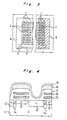
- Fig. 3 is a top plan view of a solid-state image pick-up element embodying the present invention;
- Fig. 4 is a cross-sectional view of a photoelectric transfer region of the element of Fig. 3;
- Fig. 5 is a cross-sectional view of an optical black region of the element of Fig. 3; and
- Fig. 6 is a graph indicative of the result of measurements in the amount of light leakage.
- Referring now to the drawings, there is schematically shown in Fig. 3 a solid-state image pick-up element according to an embodiment of the present invention, which comprises a large number of horizontally and vertically regularly arrayed
light receiving units 1 each comprising a pn junction photodiode, a plurality ofvertical CCD registers 2 interposed between two adjoining vertical rows of thelight receiving units 1 or otherwise formed on the left-hand side of the leftmost vertical row of thelight receiving units 1, as viewed in Fig. 3, and a horizontal CCD register 3 connected to the lower ends of thevertical CCD registers 2. This element also comprises a shielding film (shown by hatching) made of, for example, Al, AlSi or the like and covered on a portion of thelight receiving units 1. A portion not covered with the shielding film forms aphotoelectric transfer region 4 whereas another portion covered with the shielding film forms an opticalblack region 5 where the shielding film prevents light from entering. - Fig. 4 depicts the structure of the
photoelectric transfer region 4 where a plurality of n-layers 12 are formed on the surface of a p-type silicon substrate 11. The n-layers 12 are of the reverse conductivity type of the substrate 11 and correspond to thelight receiving units 1. In the proximity of the n-layers 12 are formed n--layers 13 corresponding to thevertical CCD registers 2. Achannel stopper 14 is interposed between an n-layer 12 and an n--layer 13 and is positioned on the left-hand side of the n--layer 13, as viewed in Fig. 4. A siliconoxide insulation layer 17 is formed on the substrate 11, and plural sets of two opposed first andsecond polysilicon electrodes 15 and 16 are embedded therein. A plurality of shielding films 18 are formed on the surface of the siliconoxide insulation layer 17 at locations above the second polysilicon layers 16. The shielding films 18 are made of the same material as the shielding film formed at the opticalblack region 5. Both the siliconoxide insulation layer 17 and the shielding films 18 formed thereon are entirely covered with aprotective film 19. - Fig. 5 depicts the structure of the optical
black region 5. The opticalblack region 5 has a lower structure similar to that of thephotoelectric transfer region 4 and an upper structure different from that of thephotoelectric transfer region 4. - More specifically, a plurality of n-
layers 12 are formed on the surface of the p-type silicon substrate 11. The n-layers 12 are of the reverse conductivity type of the substrate 11 and correspond to thelight receiving units 1. In the proximity of the n-layers 12 are formed n--layers 13 corresponding to thevertical CCD registers 2. Achannel stopper 14 is interposed between an n-layer 12 and an n--layer 13 and is positioned on the left-hand side of the n--layer 13, as viewed in Fig. 5. A siliconoxide insulation layer 17 is formed on the substrate 11, and plural sets of two opposed first andsecond polysilicon electrodes 15 and 16 are embedded therein. The siliconoxide insulation layer 17 is entirely covered with a shielding film 18, which is entirely covered with aprotective film 19. Furthermore, aflattening film 20 having a generally flat upper surface, ashielding layer 21, and a protective film 23 are formed in this order on theprotective film 19. Theshielding layer 21 comprises threecolor filters 21a, 21b and 21c in red, green and blue and twointermediate films 22a and 22b. Theintermediate film 22a is interposed between the lowermostred filter 21a and the middle green filter 21b whereas the intermediate film 22b is interposed between the green filter 21b and the uppermost blue filter 21c. In the formation of thecolor filters 21a-21c, a photosensitive material is initially added to gelatin, casein or the like to impart patterning properties. Thereafter, dyeing or scattering is performed by the use of appropriate dye or pigment, respectively. - The element having the above-described structure electrically operates as follows. When light enters the
photoelectric transfer region 4, signal charges are generated and accumulated in the n-layers 12 of thelight receiving units 1. Thereafter, the charges are transferred to thevertical CCD registers 2 and to the horizontal CCD register 3 by transfer clock pulses. The charges are then read out as voltage signals via anoutput portion 6 located in the proximity of the horizontal CCD register 3. - At this moment, the optical
black region 5 can restrainlight 24 from entering thelight receiving units 1 because the shielding film 18 and theshielding layer 21 including the threecolor filters 21a-21c are formed on thelight receiving units 1. If the opticalblack region 5 has no films or layers on theprotective film 19 and is subjected to heat treatment such as, for example, H2 annealing, it is likely that the shielding film 18 may cause light leakage. However, because the opticalblack region 5 has thecolor films 21a-21c above the shielding film 18, thecolor films 21a-21c attenuate the incident light 24 to the amount below 30%. In this way, the opticalblack region 5 considerably reduces the amount of theincident light 24 reaching thelight receiving units 1 via the shielding film 18. - Accordingly, the element according to the present invention can correctly detect the dark current changing with temperature, and therefore, can perform correct temperature compensation. Furthermore, because part of a large number of
light receiving units 1 are covered with a shielding layer to form the opticalblack region 5, the dynamic range in charge read units (vertical CCD registers 2) is restrained from reducing. - Fig. 6 is a graph indicative of the result of measurements in which the amount of light leakage was measured with respect to elements having a shielding layer and those having no shielding layer. Prior to the measurements, an AlSi shielding film 18 or 105 having a thickness of 1.1 µm was formed on an
insulation layer shielding layer 21 comprising threefilters 21a-21c made of gelatin and each having a thickness of 0.8 µm was formed on the shielding film 18 only. Upon application of light having an illuminance of 1500 luxes, the value of electric current generated at the photoelectric transfer region was measured by a tester. This value also includes a current value corresponding to the amount of light leakage. - As shown in the graph of Fig. 6, the relative ratio in the average amount of light leakage between the elements having a shielding layer and those having no shielding layer was 0.3:1.1. It can be readily understood from this graph that the provision of the shielding layer can considerably reduce the amount of light leakage at the optical black region.
- In applications where the present invention is applied to a solid-state image pick-up element with color filters, the color filters can be formed in the photoelectric transfer region simultaneously with those utilized as a shielding layer at the optical black region.
- In the above-described embodiment, although a shielding layer comprises three color filters in red, green and blue, the shielding layer may comprise plural filters in other colors or only one filter colored by the use of black dye.
- Moreover, the present invention is applicable to a frame transfer type solid-state image pick-up element or the like as well as an interline transfer type one. In other words, the present invention is applicable to all solid-state image pick-up elements having light receiving units formed on a semiconductor substrate, means for sequentially reading signals obtained through photoelectric transfer, and an optical black region formed at a portion thereof.
- As is clear from the above, because a solid-state image pick-up element according to the present invention is provided with a shielding layer at an optical black region covered with a shielding film, the optical black region can prevent light leakage to light receiving units, thereby correctly compensating an output value from an photoelectric transfer region for the amount of changes with temperature and preventing the dynamic range in charge read units from reducing.
- Furthermore, color filters serviceable as a shielding layer of the optical black region can be readily formed merely by changing photomasks, and therefore, no additional processes are needed.
Claims (3)
- A solid-state image pick-up device comprising an array of photoelectric elements (1) formed on a semiconductor substrate (11), transfer means (2,3,15,16) for effecting transfer of photoelectrically generated charges in a transfer region of the array so as to read out image-defining electrical signals, said transfer means including charge transfer control electrodes (15,16) formed on said substrate, a first shielding film (18) defining an optical black region in which the photoelectric elements (1) are shielded from incident light, wherein said first shielding film (18) overlies said electrodes (15,16) and undulates accordingly, a flattening layer (20) disposed over the undulating first shielding film (18) and having a substantially flat upper surface, and a second shielding film (21) formed over said flattening layer (20) for reducing the amount of said incident light reaching the first shielding film (18).
- A solid-state image pick-up device according to claim 1, wherein said second shielding film (21) comprises plural layers constituting respective color filters (21a,21b,21c).
- A solid-state image pick-up device according to claim 2, comprising three said layers constituting respective color filters (21a,21b,21c) of red, green and blue.
Applications Claiming Priority (2)
| Application Number | Priority Date | Filing Date | Title |
|---|---|---|---|
| JP3139996A JP2710292B2 (en) | 1991-06-12 | 1991-06-12 | Solid-state imaging device |
| JP139996/91 | 1991-06-12 |
Publications (2)
| Publication Number | Publication Date |
|---|---|
| EP0518686A1 EP0518686A1 (en) | 1992-12-16 |
| EP0518686B1 true EP0518686B1 (en) | 1997-09-17 |
Family
ID=15258507
Family Applications (1)
| Application Number | Title | Priority Date | Filing Date |
|---|---|---|---|
| EP92305420A Expired - Lifetime EP0518686B1 (en) | 1991-06-12 | 1992-06-12 | Solid state image pick-up device |
Country Status (5)
| Country | Link |
|---|---|
| US (1) | US5455624A (en) |
| EP (1) | EP0518686B1 (en) |
| JP (1) | JP2710292B2 (en) |
| KR (1) | KR960010932B1 (en) |
| DE (1) | DE69222230T2 (en) |
Families Citing this family (11)
| Publication number | Priority date | Publication date | Assignee | Title |
|---|---|---|---|---|
| US5521639A (en) * | 1992-04-30 | 1996-05-28 | Sony Corporation | Solid-state imaging apparatus including a reference pixel in the optically-black region |
| JPH05343656A (en) * | 1992-06-09 | 1993-12-24 | Matsushita Electron Corp | Image sensor |
| JP3550599B2 (en) * | 1994-02-03 | 2004-08-04 | 株式会社ニコン | Image sensor system |
| US20010012067A1 (en) * | 1996-04-12 | 2001-08-09 | Stuart M. Spitzer | High definition television progressive scan broadcast camera |
| US6721005B1 (en) * | 1998-12-03 | 2004-04-13 | Sony Corporation | Solid state image sensor having different structures for effective pixel area and optical black area |
| US6376274B1 (en) * | 1999-06-25 | 2002-04-23 | United Microelectronics Corp. | Process for producing photosensor with color filter |
| FR2802298B1 (en) | 1999-12-14 | 2002-03-08 | Cie Du Sol | INJECTION COLUMN DIAMETER CONTROL METHOD |
| EP1176808A3 (en) * | 2000-07-27 | 2003-01-02 | Canon Kabushiki Kaisha | Image sensing apparatus |
| JP4018456B2 (en) * | 2002-06-03 | 2007-12-05 | 富士フイルム株式会社 | Imaging device |
| EP1890479A1 (en) * | 2006-08-17 | 2008-02-20 | STMicroelectronics (Research & Development) Limited | Imaging Device with Heat-Shielding Means for Inhibiting Thermal Damage to a Lens |
| WO2020053975A1 (en) * | 2018-09-11 | 2020-03-19 | シャープ株式会社 | Light-emitting device |
Family Cites Families (15)
| Publication number | Priority date | Publication date | Assignee | Title |
|---|---|---|---|---|
| JPS55125685A (en) * | 1979-03-22 | 1980-09-27 | Dainippon Printing Co Ltd | Manufacture of color solid image taking element board |
| JPS5830284A (en) * | 1981-08-17 | 1983-02-22 | Nec Corp | solid-state imaging device |
| JPS5870685A (en) * | 1981-10-22 | 1983-04-27 | Nec Corp | Solid-state image pickup device |
| JPS58125968A (en) * | 1982-01-22 | 1983-07-27 | Nec Corp | solid state imaging device |
| JPS58209160A (en) * | 1982-05-31 | 1983-12-06 | Hitachi Ltd | Solid-state image pickup element |
| JPS5917778A (en) * | 1982-07-21 | 1984-01-30 | Toshiba Corp | Solid-state image pickup device and its production |
| US4649430A (en) * | 1985-08-27 | 1987-03-10 | Texas Instruments, Incorporated | CCD imager with many dummy pixels |
| JPS63185058A (en) * | 1987-01-28 | 1988-07-30 | Hitachi Ltd | solid-state image sensor |
| EP0289044B1 (en) * | 1987-04-30 | 1997-03-19 | Kabushiki Kaisha Toshiba | Color image sensor and manufacturing method thereof |
| US4876167A (en) * | 1987-08-20 | 1989-10-24 | Eastman Kodak Company | Color filter array containing a photocrosslinked polymeric mordant |
| JP2697002B2 (en) * | 1988-10-14 | 1998-01-14 | 日本電気株式会社 | Method for manufacturing color solid-state imaging device |
| JP2871760B2 (en) * | 1989-11-28 | 1999-03-17 | 日本電気株式会社 | Solid-state imaging device |
| US5140396A (en) * | 1990-10-10 | 1992-08-18 | Polaroid Corporation | Filter and solid state imager incorporating this filter |
| JP3125303B2 (en) * | 1990-11-26 | 2001-01-15 | 日本電気株式会社 | Solid-state imaging device |
| JPH04199876A (en) * | 1990-11-29 | 1992-07-21 | Nec Corp | Solid state image sensing device and manufacture thereof |
-
1991
- 1991-06-12 JP JP3139996A patent/JP2710292B2/en not_active Expired - Lifetime
-
1992
- 1992-06-09 KR KR1019920009978A patent/KR960010932B1/en not_active Expired - Lifetime
- 1992-06-12 DE DE69222230T patent/DE69222230T2/en not_active Expired - Lifetime
- 1992-06-12 EP EP92305420A patent/EP0518686B1/en not_active Expired - Lifetime
-
1994
- 1994-01-19 US US08/183,917 patent/US5455624A/en not_active Expired - Lifetime
Also Published As
| Publication number | Publication date |
|---|---|
| EP0518686A1 (en) | 1992-12-16 |
| KR930001446A (en) | 1993-01-16 |
| KR960010932B1 (en) | 1996-08-13 |
| DE69222230D1 (en) | 1997-10-23 |
| US5455624A (en) | 1995-10-03 |
| DE69222230T2 (en) | 1998-03-19 |
| JP2710292B2 (en) | 1998-02-10 |
| JPH04364779A (en) | 1992-12-17 |
Similar Documents
| Publication | Publication Date | Title |
|---|---|---|
| US7554587B2 (en) | Color solid-state image pickup device | |
| US7742088B2 (en) | Image sensor and digital camera | |
| US5121192A (en) | Solid-state color imaging device | |
| EP0015711B1 (en) | Colour image sensing | |
| CN101355093B (en) | Color filter array and its applied image sensing device | |
| US4412236A (en) | Color solid-state imager | |
| US7208811B2 (en) | Photo-detecting device | |
| US8072007B2 (en) | Backside-illuminated imaging device | |
| CN212343888U (en) | Image sensor and electronic equipment | |
| US5455624A (en) | Solid image pick-up element | |
| JPH09116127A (en) | Solid-state imaging device | |
| US7656446B2 (en) | CCD color solid-state image pickup device | |
| US7126099B2 (en) | Image sensor with improved uniformity of effective incident light | |
| US5238856A (en) | Method of manufacturing solid-state image pick-up device | |
| US4783691A (en) | Color solid-state image sensor | |
| US5237185A (en) | Image pickup apparatus with different gate thicknesses | |
| EP0557135B1 (en) | Image sensor color filters | |
| EP0040984B1 (en) | Method of producing solid-state color imaging devices | |
| EP0066767B1 (en) | Solid state image sensor | |
| US5614950A (en) | CCD image sensor and method of preventing a smear phenomenon in the sensor | |
| US5635738A (en) | Infrared solid-state image sensing apparatus | |
| JPH05175471A (en) | Solid-state image sensing device | |
| JPH04343470A (en) | Solid-state image pickup device | |
| KR100555480B1 (en) | Solid static pick-up device having microlens and method for manufacturing the same | |
| JPH0794694A (en) | Solid-state image sensor |
Legal Events
| Date | Code | Title | Description |
|---|---|---|---|
| PUAI | Public reference made under article 153(3) epc to a published international application that has entered the european phase |
Free format text: ORIGINAL CODE: 0009012 |
|
| AK | Designated contracting states |
Kind code of ref document: A1 Designated state(s): DE FR GB NL |
|
| 17P | Request for examination filed |
Effective date: 19930205 |
|
| 17Q | First examination report despatched |
Effective date: 19951002 |
|
| GRAG | Despatch of communication of intention to grant |
Free format text: ORIGINAL CODE: EPIDOS AGRA |
|
| GRAH | Despatch of communication of intention to grant a patent |
Free format text: ORIGINAL CODE: EPIDOS IGRA |
|
| GRAH | Despatch of communication of intention to grant a patent |
Free format text: ORIGINAL CODE: EPIDOS IGRA |
|
| GRAA | (expected) grant |
Free format text: ORIGINAL CODE: 0009210 |
|
| AK | Designated contracting states |
Kind code of ref document: B1 Designated state(s): DE FR GB NL |
|
| REF | Corresponds to: |
Ref document number: 69222230 Country of ref document: DE Date of ref document: 19971023 |
|
| ET | Fr: translation filed | ||
| PLBE | No opposition filed within time limit |
Free format text: ORIGINAL CODE: 0009261 |
|
| STAA | Information on the status of an ep patent application or granted ep patent |
Free format text: STATUS: NO OPPOSITION FILED WITHIN TIME LIMIT |
|
| 26N | No opposition filed | ||
| REG | Reference to a national code |
Ref country code: GB Ref legal event code: IF02 |
|
| PGFP | Annual fee paid to national office [announced via postgrant information from national office to epo] |
Ref country code: FR Payment date: 20110621 Year of fee payment: 20 |
|
| PGFP | Annual fee paid to national office [announced via postgrant information from national office to epo] |
Ref country code: GB Payment date: 20110608 Year of fee payment: 20 Ref country code: NL Payment date: 20110629 Year of fee payment: 20 |
|
| PGFP | Annual fee paid to national office [announced via postgrant information from national office to epo] |
Ref country code: DE Payment date: 20110608 Year of fee payment: 20 |
|
| REG | Reference to a national code |
Ref country code: DE Ref legal event code: R071 Ref document number: 69222230 Country of ref document: DE |
|
| REG | Reference to a national code |
Ref country code: DE Ref legal event code: R071 Ref document number: 69222230 Country of ref document: DE |
|
| REG | Reference to a national code |
Ref country code: NL Ref legal event code: V4 Effective date: 20120612 |
|
| REG | Reference to a national code |
Ref country code: GB Ref legal event code: PE20 Expiry date: 20120611 |
|
| PG25 | Lapsed in a contracting state [announced via postgrant information from national office to epo] |
Ref country code: DE Free format text: LAPSE BECAUSE OF EXPIRATION OF PROTECTION Effective date: 20120613 |
|
| PG25 | Lapsed in a contracting state [announced via postgrant information from national office to epo] |
Ref country code: GB Free format text: LAPSE BECAUSE OF EXPIRATION OF PROTECTION Effective date: 20120611 |