EP0507686B1 - Automatische Anordnung zur Phasenverriegelung eines Ausgangssignals einer Schaltung - Google Patents
Automatische Anordnung zur Phasenverriegelung eines Ausgangssignals einer Schaltung Download PDFInfo
- Publication number
- EP0507686B1 EP0507686B1 EP92400924A EP92400924A EP0507686B1 EP 0507686 B1 EP0507686 B1 EP 0507686B1 EP 92400924 A EP92400924 A EP 92400924A EP 92400924 A EP92400924 A EP 92400924A EP 0507686 B1 EP0507686 B1 EP 0507686B1
- Authority
- EP
- European Patent Office
- Prior art keywords
- loop
- phase
- slow
- circuit
- fast
- Prior art date
- Legal status (The legal status is an assumption and is not a legal conclusion. Google has not performed a legal analysis and makes no representation as to the accuracy of the status listed.)
- Expired - Lifetime
Links
- 230000010363 phase shift Effects 0.000 claims description 17
- 238000001514 detection method Methods 0.000 claims description 12
- 230000001052 transient effect Effects 0.000 claims description 2
- 238000010586 diagram Methods 0.000 description 9
- 230000001934 delay Effects 0.000 description 3
- 230000003321 amplification Effects 0.000 description 2
- 230000003111 delayed effect Effects 0.000 description 2
- 238000001914 filtration Methods 0.000 description 2
- 238000003199 nucleic acid amplification method Methods 0.000 description 2
- 241001415961 Gaviidae Species 0.000 description 1
- 238000000429 assembly Methods 0.000 description 1
- 230000005540 biological transmission Effects 0.000 description 1
- 230000015572 biosynthetic process Effects 0.000 description 1
- 238000010276 construction Methods 0.000 description 1
- 238000013016 damping Methods 0.000 description 1
- 238000002347 injection Methods 0.000 description 1
- 239000007924 injection Substances 0.000 description 1
- 230000003071 parasitic effect Effects 0.000 description 1
- 239000007787 solid Substances 0.000 description 1
- 230000001360 synchronised effect Effects 0.000 description 1
- 210000003462 vein Anatomy 0.000 description 1
Images



Classifications
-
- H—ELECTRICITY
- H03—ELECTRONIC CIRCUITRY
- H03L—AUTOMATIC CONTROL, STARTING, SYNCHRONISATION OR STABILISATION OF GENERATORS OF ELECTRONIC OSCILLATIONS OR PULSES
- H03L7/00—Automatic control of frequency or phase; Synchronisation
-
- H—ELECTRICITY
- H03—ELECTRONIC CIRCUITRY
- H03L—AUTOMATIC CONTROL, STARTING, SYNCHRONISATION OR STABILISATION OF GENERATORS OF ELECTRONIC OSCILLATIONS OR PULSES
- H03L7/00—Automatic control of frequency or phase; Synchronisation
- H03L7/06—Automatic control of frequency or phase; Synchronisation using a reference signal applied to a frequency- or phase-locked loop
- H03L7/08—Details of the phase-locked loop
- H03L7/0805—Details of the phase-locked loop the loop being adapted to provide an additional control signal for use outside the loop
-
- H—ELECTRICITY
- H03—ELECTRONIC CIRCUITRY
- H03L—AUTOMATIC CONTROL, STARTING, SYNCHRONISATION OR STABILISATION OF GENERATORS OF ELECTRONIC OSCILLATIONS OR PULSES
- H03L7/00—Automatic control of frequency or phase; Synchronisation
- H03L7/06—Automatic control of frequency or phase; Synchronisation using a reference signal applied to a frequency- or phase-locked loop
- H03L7/08—Details of the phase-locked loop
- H03L7/081—Details of the phase-locked loop provided with an additional controlled phase shifter
- H03L7/0812—Details of the phase-locked loop provided with an additional controlled phase shifter and where no voltage or current controlled oscillator is used
Definitions
- the present invention relates to an automatic phase control device of a circuit.
- a phase control device used in particular for an amplification chain in class C.
- This device comprises one or more control loops. The propagation times between the direct chain and the return chain are adjusted manually. This device works very well, but the pre-positioning of the control loops must be carried out manually, which does not allow total interchangeability of the circuit to be controlled in phase.
- the subject of the present invention is a device for controlling the phase of an output signal of a circuit on the phase of the input signal of this circuit, device allowing automatic pre-positioning, which is capable of converging in practically all circumstances, which ensures slaving even in the event of very slow and monotonous variations of phase disturbances, over a very wide range of frequencies, with a very short time for locking the correction of disturbances.
- the device according to the invention comprises a so-called “slow” loop, comprising a delay line in cascade, an amplifier, a phase shifter, a 0/180 ° inverter, a filter and a device for detecting overshoot of phase thresholds. and inverter control.
- the phase control system of the invention preferably consists of two control loops, a fast loop and a slow loop.
- the fast loop corrects rapid disturbances of the transient and phase noise type, the variations of which are taken into account, in the case of Doppler processing, and therefore undesirable. It must therefore be very fast in order to maintain the widest possible correction band, on the other hand, it must be sufficiently stable in the sense of damping not to generate parasitic pulses itself. In the same vein, it must be quiet so as not to bring back more phase noise than it corrects.
- the function of the slow loop is to allow the fast loop to operate in the best possible conditions. It must equalize the delays between direct chain and reference so as to ensure the convergence of the fast loop. It must also equalize the phase so as to bring the average of the phase difference in the middle of the catch-up characteristic of the fast loop, in order to provide the latter with the maximum correction range and efficiency.
- the slow loop thus ensures the best conditions operating at the fast loop for the widest possible range of disturbance values and propagation delay of the direct chain.
- the servo system consists first of all of a fast loop BR comprising a fast loop phase shifter 2, a direct chain 3, a coupler 4, a phase shift meter 6, a fast loop filter 7, and an amplifier fast loop 8.
- the input phase ⁇ e ( ⁇ ) is corrected by ⁇ using the fast loop phase shifter 2, in the direct chain.
- the direct chain 3 is modeled in phase characteristics by a propagation delay ⁇ and a perturbation ⁇ ( ⁇ ).
- the output phase of the direct chain 3 is sampled using a coupler 4.
- the difference between the value measured at the output of the direct chain 3 and the setpoint is carried out by means of a phase meter.
- This error signal is then filtered using a fast loop filter 7 of transfer function F ( ⁇ ).
- This signal is then amplified by the fast loop amplifier 8.
- a pre-positioning signal can be injected to improve the performance of the fast loop.
- the fast loop correction signal is finally fed back into the direct chain using the fast loop phase shifter 8.
- the fast loop setpoint is generated at the coupler 1, delay line 5, loop phase shifter assembly slow 9, 0/180 ° inverter and phase shift meter 6.
- the input phase ⁇ e ( ⁇ ) is taken at the input of the direct chain so as to generate the setpoint signal.
- This signal is delayed in time by a delay ⁇ ′ using a delay line 5. It is then phase shifted through the slow loop phase shifter 9 and the inverter 0/180 ° 10.
- L ' LRV assembly comprising the delay line 5, the slow loop phase shifter 9 and the inverter 0/180 ° 10 constitutes a variable delay line.
- the adjustment of the delay used to generate the setpoint is controlled by the slow loop consisting of the slow loop phase shifter 9, inverter 0/180 ° 10, slow loop filter 11, slow loop amplifier 12 and its device. detection and control 13.
- the correction to be made is the equalization of the propagation times between the direct chain and the path of the setpoint signal in the fast loop.
- the output phase ⁇ S ( ⁇ ) is used as the setpoint signal for the slow loop and the signal at the output of the inverter 0/180 ° is controlled on this phase by means of the slow loop.
- the phase difference thus obtained at the output of the phase shift meter 6 is firstly filtered using the slow loop filter 11 and then amplified by the slow loop amplifier 12. The signal thus obtained is fed back into the variable delay line LRV assembly by means of the slow loop phase shifter 9.
- the variable delay line comprises a fixed delay line 5 and a slow loop phase shifter 9 of finite dynamics.
- the detection and control device 13 determines the state of the slow loop phase shifter 9 based on the value of the control signal thereof coming from the slow loop amplifier 12. From this information, the detection device and control 13 generates two punctual actions over time. If the phase shifter comes into abutment, which corresponds to a phase catching close to + or - ⁇ radians, the device 13 phase the signal by + or - ⁇ radians using the 0/180 ° inverter 10.
- the slow loop therefore controls the same phase as before the action of the detection and control 13 but to within 2 ⁇ radians and having brought the slow loop phase shifter 9 to the middle of the characteristic.
- the slow loop can operate autonomously, without the fast loop.
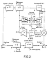
- FIG. 2 shows the construction details of the device 13, as well as the elements of the servo device necessary for the explanations.
- the input phase ⁇ e ( ⁇ ) is sampled by means of the coupler 1. This input phase is delayed by a delay ⁇ ′ equivalent to the propagation delay ⁇ of the direct chain 3.
- the phase shift meter 6 generates a error signal which is filtered and amplified using the slow loop filter 11 and the slow loop amplifier 12. The resulting signal is fed back in the form of a phase shift ⁇ into the slow loop phase shifter 9. If this phase shift ⁇ comes to approach the stops of the phase shifter, the detection and control device 13 comes into action.
- This action is implemented by three sub-assemblies 13a to 13c that the device includes 13.
- the sub-assembly 13a of the comparator type, detects if the phase shift ⁇ exceeds limit values ⁇ max, ⁇ min fixed to the dynamics of the phase shifter (minus a certain safety margin).
- the logic signal thus generated is possibly synchronized with a signal outside the slow loop by means of the device 13b.
- the resulting signal is used for resetting the value integrated by the slow loop filter 11.
- a flip-flop device 13c is rocked which controls the inverter 0/180 ° 10.
- the rocker 13c can also receive, if necessary, a synchronization signal.
- the slow loop can operate autonomously (without fast loop).
- the main track includes: the phase shifter 9, the inverter 0/180 ° 10 and the direct chain 3 (which is likely to be subjected to disturbances ⁇ ).
- a coupler 1 takes the input phase and is connected by a delay line (delay ⁇ ′) to the phase meter 6, which is also connected to the output coupler 4.
- the error signal from the phase meter 6 is sent, via the loop filter 11, to the slow loop amplifier 12 whose output is connected to the phase shifter 9 and to the detection and control device 13.
- This device 13 is connected to the filter 11 and to the inverter 10, and can optionally receive a synchronization signal.
- the filter 7 of fast loop can either be a specific component, or result from the characteristics of limitation of the passband components used by other circuits in the loop.
- the fast loop phase shifter can be either analog (with continuous phase shift), or digital with discrete phase shift, or a combination of the two.
- the processing implemented by the fast loop filter 7 and the fast loop amplifier 8 can be either analog or digital, or a combination of the two, and this processing can be done in sampled / blocked mode. You can optionally add a prepositioning signal to it.
- the order of elements 7 and 8 is arbitrary.
- the slow loop consists of: the coupler 1, the delay line 5, the phase shifter 9, the inverter 0/180 °, the filter 11, the amplifier 12 and the detection and control device 13.
- the filter 11 can either be a specific component or result from the characteristics of limitation of the passband of the components used for other circuits of the loop.
- the phase shifter 9 can be either analog with continuous variation of the phase shifts, or digital with discrete variation of the phase shifts, or a combination of the two.
- the 0/180 ° inverter can be either a phase shifter or a logic inverter.
- the order of elements 5, 9 and 10 is arbitrary.
- the processing implemented by: the filter 11, and the amplifier 12 can be analog or digital, or a combination of the two, or alternatively in sampled / blocked mode.
- the order of the elements of the filter 11 and amplifier 12 slow loop chain is arbitrary.
- the device according to the invention automatically slaves to 2k ⁇ radians near the phase of the input signal without having to make a manual adjustment or an adjustment case by case.
- the circuit 13 provides convergence at 2k ⁇ radians near the slow loop.
- This circuit 13 generates from the information on the state of the phase shifter 9 actions whose purpose is the convergence of the slow loop.
- the first action consists in introducing an additional phase shift of + or - 180 ° by command of the inverter 10.
- the second action consists in forcing punctually to zero the value integrated by the filter 11.
- the result of these two actions is that the loop slow is slaved to 2 ⁇ radians on the middle phase characteristic of the phase shifter 9.
- the device of the invention tends to automatically equalize the propagation delays between chain to be slaved (comprising element 3) and setpoint chain (slow loop).
- the device of the invention can be used for example for controlling the phase transfer function of an amplification chain with solid state components or with a tube (Magnetron, Klystron, ...), for a servo phase shifter, in a phase modulation / demodulation device, for the formation of beams with servo phase shifters, etc.
- FIG. 4 shows the equivalent diagram of the direct chain. It comprises, between the input coupler 1 and the output coupler 4, the direct chain 3 having a delay ⁇ and the phase shifter 2, providing a phase shift of ⁇ .
- the order of elements 2 and 3 is unimportant.
- the equivalent diagram of the fast loop of FIG. 5 includes: the phase meter 6, the fast loop amplifier 8 (of delay ⁇ ⁇ and of gain K) and the fast loop filter 7 (of filtering function F) .
- the equivalent slow loop diagram shown in FIG. 6, includes the slow loop amplifier 12 (of gain K) and the filter 11 (of filtering function F ′).
- FIG. 7 shows the block diagram of a principle of a variant of the device of the invention, according to which the slow loop acts on the overall correction factor, because some of its elements are inserted in the direct chain.
- the direct chain comprises, between the input coupler 1 and the output coupler 4, the slow loop phase shifter 9, the inverter 0/180 ° 10, the fast loop phase shifter 7 and the direct chain 3.
- the couplers 4 and 1 connect the phase meter 6 and the delay line 5
- the output of the phase shift meter 6 is connected on the one hand to a fast loop comprising the filter 7 and the amplifier 8, and on the other hand to the slow loop comprising the filter 11 and the amplifier 12 and to the inputs of the inverter 10 and the filter 11.
Landscapes
- Stabilization Of Oscillater, Synchronisation, Frequency Synthesizers (AREA)
- Amplifiers (AREA)
Claims (7)
- Automatische Vorrichtung zur Regelung der Phase eines Ausgangssignals einer Schaltung auf die Phase des Eingangssignals dieser Schaltung, wobei diese Vorrichtung von dem Typ ist, der wenigstens eine Regelschleife parallel zu der zu regelnden Schaltung (3) aufweist, dadurch gekennzeichnet, daß sie eine sogenannte "langsame" Schleife mit einer Verzögerungsleitung (5), einem Verstärker (12), einem Phasenschieber (9), einem 0/180°-Umschalter (10), einem Filter (11) und einer Einrichtung (13) zum Erfassen der Überschreitung von Phasenschwellenwerten und zur Steuerung des Umschalters aufweist.
- Vorrichtung nach Anspruch 1, dadurch gekennzeichnet, daß die Einrichtung zur Erfassung und zur Steuerung eine Schaltung (13a) zum Erfassen der Überschreitung von Phasenschwellenwerten aufweist, die mit dem Ausgang (12) des Verstärkers der "langsamen" Schleife und mit dem Eingang eines Kippglieds (13c) verbunden ist, das den 0/180°-Umschalter steuert.
- Vorrichtung nach Anspruch 2, dadurch gekennzeichnet, daß eine Schaltung (13b) zur Synchronisierung mit einem äußeren Signal zwischen die Erfassungsschaltung (13a) und das Kippglied (13c) eingefügt ist.
- Vorrichtung nach einem der vorhergehenden Ansprüche, dadurch gekennzeichnet, daß ein Phasenverschiebungsmesser (6) zwischen dem Ausgang (4) der zu regelnden Schaltung und der Verzögerungsleitung (5) angeordnet und mit dem Eingang der "langsamen" Schleife verbunden ist.
- Vorrichtung nach einem der vorhergehenden Ansprüche, dadurch gekennzeichnet, daß sich das Filter aus den Charakteristika der Begrenzung des Durchlaßbereichs der Bauteile ergibt, die von anderen Schaltungen der Schleife verwendet werden.
- Vorrichtung nach einem der vorhergehenden Ansprüche, dadurch gekennzeichnet, daß sie einem "schnellen" Regelkreis (2, 7, 8) zugeordnet ist, der die Korrektur von schnellen Störungen des transienten Typs und Phasenrauschen ermöglicht.
- Vorrichtung nach Anspruch 6, dadurch gekennzeichnet, daß Elemente (9, 10) der "langsamen" Schleife in die geregelte Schaltung eingefügt sind.
Applications Claiming Priority (2)
| Application Number | Priority Date | Filing Date | Title |
|---|---|---|---|
| FR9104163 | 1991-04-05 | ||
| FR9104163A FR2674995B1 (fr) | 1991-04-05 | 1991-04-05 | Dispositif automatique d'asservissement de phase d'un circuit. |
Publications (2)
| Publication Number | Publication Date |
|---|---|
| EP0507686A1 EP0507686A1 (de) | 1992-10-07 |
| EP0507686B1 true EP0507686B1 (de) | 1994-12-07 |
Family
ID=9411518
Family Applications (1)
| Application Number | Title | Priority Date | Filing Date |
|---|---|---|---|
| EP92400924A Expired - Lifetime EP0507686B1 (de) | 1991-04-05 | 1992-04-02 | Automatische Anordnung zur Phasenverriegelung eines Ausgangssignals einer Schaltung |
Country Status (8)
| Country | Link |
|---|---|
| US (1) | US5216698A (de) |
| EP (1) | EP0507686B1 (de) |
| JP (1) | JPH05160723A (de) |
| KR (1) | KR100212363B1 (de) |
| CA (1) | CA2064964A1 (de) |
| DE (1) | DE69200796T2 (de) |
| ES (1) | ES2065140T3 (de) |
| FR (1) | FR2674995B1 (de) |
Families Citing this family (3)
| Publication number | Priority date | Publication date | Assignee | Title |
|---|---|---|---|---|
| US5351015A (en) * | 1993-02-03 | 1994-09-27 | Silicon Systems, Inc. | Time based data separator zone change sequence |
| SE510713C2 (sv) * | 1997-10-10 | 1999-06-14 | Ericsson Telefon Ab L M | Faslåsningskrets samt metod för reglering av spänningsstyrd oscillator |
| KR100331562B1 (ko) * | 1999-11-29 | 2002-04-06 | 윤종용 | 지연 동기 루프 회로 및 내부 클럭 신호 발생 방법 |
Family Cites Families (7)
| Publication number | Priority date | Publication date | Assignee | Title |
|---|---|---|---|---|
| US4298986A (en) * | 1979-12-26 | 1981-11-03 | General Electric Company | Receiver for phase-shift modulated carrier signals |
| GB2110893B (en) * | 1981-12-04 | 1985-10-16 | Philips Electronic Associated | Controlled-phase system |
| US4691176A (en) * | 1986-03-17 | 1987-09-01 | General Electric Company | Adaptive carrier tracking circuit |
| NL8602626A (nl) * | 1986-10-20 | 1988-05-16 | Philips Nv | Klokopwekking in transmissiestelsel met sterke bandbreedtebegrenzing. |
| US4733404A (en) * | 1986-11-25 | 1988-03-22 | Hewlett-Packard Company | Apparatus and method for signal processing |
| FR2639775A1 (fr) * | 1988-11-25 | 1990-06-01 | Thomson Csf | Dispositif de correction de phase induite par le fonctionnement en classe c de l'amplificateur " etat solide " et chaine radar utilisant un tel dispositif |
| US5018170A (en) * | 1989-11-21 | 1991-05-21 | Unisys Corporation | Variable data rate clock synthesizer |
-
1991
- 1991-04-05 FR FR9104163A patent/FR2674995B1/fr not_active Expired - Fee Related
-
1992
- 1992-03-30 US US07/860,157 patent/US5216698A/en not_active Expired - Fee Related
- 1992-04-02 ES ES92400924T patent/ES2065140T3/es not_active Expired - Lifetime
- 1992-04-02 JP JP4108455A patent/JPH05160723A/ja not_active Withdrawn
- 1992-04-02 EP EP92400924A patent/EP0507686B1/de not_active Expired - Lifetime
- 1992-04-02 DE DE69200796T patent/DE69200796T2/de not_active Expired - Fee Related
- 1992-04-02 CA CA002064964A patent/CA2064964A1/fr not_active Abandoned
- 1992-04-03 KR KR1019920005568A patent/KR100212363B1/ko not_active Expired - Fee Related
Also Published As
| Publication number | Publication date |
|---|---|
| FR2674995B1 (fr) | 1993-06-11 |
| FR2674995A1 (fr) | 1992-10-09 |
| DE69200796T2 (de) | 1995-04-13 |
| CA2064964A1 (fr) | 1992-10-06 |
| DE69200796D1 (de) | 1995-01-19 |
| US5216698A (en) | 1993-06-01 |
| EP0507686A1 (de) | 1992-10-07 |
| KR100212363B1 (ko) | 1999-08-02 |
| KR920020857A (ko) | 1992-11-21 |
| ES2065140T3 (es) | 1995-02-01 |
| JPH05160723A (ja) | 1993-06-25 |
Similar Documents
| Publication | Publication Date | Title |
|---|---|---|
| EP0192061B1 (de) | Einrichtung zur automatischen Verstärkungsregelung eines T.D.M.A.-Empfängers | |
| EP0500473B1 (de) | Phasen/Frequenzkomparator für Taktrückgewinnungssystem | |
| EP0077224A1 (de) | System zur Lageeinstellung mit Kraftrückführung und mit Übertragungsverzögerung und Anwendung bei einem Fernmanipulator | |
| FR2834395A1 (fr) | Procede et dispositif de stabilisation d'une boucle a verrouillage de phase | |
| FR2952197A1 (fr) | Dispositif de generation de signaux d'horloge a comparaison asymetrique d'erreurs de phase | |
| EP0187067B1 (de) | Umschaltungssystem für ein digitales Übertragungsnetz | |
| EP0238141A1 (de) | Empfänger für frequenzmodulierte Signale | |
| EP0115234B1 (de) | Verfahren und Schaltung zur Frequenz- und Phasenverkopplung eines örtlichen Oszillators im Fernsehen | |
| FR2746994A1 (fr) | Estimateur et recuperateur de phase robuste pour signaux numeriques affectes notamment de gigue de phase | |
| FR2728118A1 (fr) | Comparateur de phase entre un signal numerique et un signal d'horloge, et boucle a verrouillage de phase correspondante | |
| EP0507686A1 (de) | Automatische Anordnung zur Phasenverriegelung eines Ausgangssignals einer Schaltung | |
| EP0130260A1 (de) | Schnittstellenmodul für Fernsprechleitungen | |
| EP0661833A1 (de) | Basisband-Amplitude/Frequenz-Charakteristikschätzer | |
| EP0246135A1 (de) | Phasen- und Frequenzdetektor und seine Anwendung in einer Phasenregelschleife | |
| EP0991193A1 (de) | Funkgerät mit einem Frequenzsynthetisierer und Phasendiskriminator für ein solches Gerät | |
| EP0503416B1 (de) | Demodulator mit Phasenregelschleife | |
| EP0347985B1 (de) | Allpasstyp-Schaltung für ultrahohe Frequenzen | |
| EP0415316B1 (de) | Vorrichtung zur Rückgewinnung eines Trägers mit einer Costas-Schleife | |
| FR2833430A1 (fr) | Amplificateur differentiel a faible niveau de bruit | |
| EP0748093A1 (de) | Digitales Übertragungssystem mit Entscheidungsmitteln zur Auswahl der Synchronisierungsart | |
| JPH05183590A (ja) | タイミング再生装置 | |
| EP1100201B1 (de) | Digitaler Phasenregelkreis | |
| FR2552959A1 (fr) | Circuit de recuperation d'une onde porteuse muni d'un moyen d'aide a l'acquisition automatique et rapide | |
| FR2879858A1 (fr) | Procede de correction du dephasage entre deux signaux d'enree d'une boucle a verrouillage de phase et dispositif associe | |
| EP0309306B1 (de) | Verfahren zur Detektion eines Phasenfehlers zwischen Referenzsignal und zu demodulierendem Signal bei kohärenter digitaler Demodulation und Vorrichtung zur Durchführung des Verfahrens |
Legal Events
| Date | Code | Title | Description |
|---|---|---|---|
| PUAI | Public reference made under article 153(3) epc to a published international application that has entered the european phase |
Free format text: ORIGINAL CODE: 0009012 |
|
| AK | Designated contracting states |
Kind code of ref document: A1 Designated state(s): DE ES FR GB NL |
|
| 17P | Request for examination filed |
Effective date: 19930327 |
|
| 17Q | First examination report despatched |
Effective date: 19930429 |
|
| RAP1 | Party data changed (applicant data changed or rights of an application transferred) |
Owner name: THOMSON-CSF |
|
| RAP3 | Party data changed (applicant data changed or rights of an application transferred) |
Owner name: THOMSON-CSF |
|
| GRAA | (expected) grant |
Free format text: ORIGINAL CODE: 0009210 |
|
| AK | Designated contracting states |
Kind code of ref document: B1 Designated state(s): DE ES FR GB NL |
|
| REF | Corresponds to: |
Ref document number: 69200796 Country of ref document: DE Date of ref document: 19950119 |
|
| REG | Reference to a national code |
Ref country code: ES Ref legal event code: FG2A Ref document number: 2065140 Country of ref document: ES Kind code of ref document: T3 |
|
| GBT | Gb: translation of ep patent filed (gb section 77(6)(a)/1977) |
Effective date: 19950210 |
|
| PLBE | No opposition filed within time limit |
Free format text: ORIGINAL CODE: 0009261 |
|
| STAA | Information on the status of an ep patent application or granted ep patent |
Free format text: STATUS: NO OPPOSITION FILED WITHIN TIME LIMIT |
|
| 26N | No opposition filed | ||
| PGFP | Annual fee paid to national office [announced via postgrant information from national office to epo] |
Ref country code: NL Payment date: 20010314 Year of fee payment: 10 |
|
| PGFP | Annual fee paid to national office [announced via postgrant information from national office to epo] |
Ref country code: DE Payment date: 20010319 Year of fee payment: 10 |
|
| PGFP | Annual fee paid to national office [announced via postgrant information from national office to epo] |
Ref country code: GB Payment date: 20010321 Year of fee payment: 10 |
|
| PGFP | Annual fee paid to national office [announced via postgrant information from national office to epo] |
Ref country code: ES Payment date: 20010410 Year of fee payment: 10 |
|
| PGFP | Annual fee paid to national office [announced via postgrant information from national office to epo] |
Ref country code: FR Payment date: 20010424 Year of fee payment: 10 |
|
| REG | Reference to a national code |
Ref country code: GB Ref legal event code: IF02 |
|
| PG25 | Lapsed in a contracting state [announced via postgrant information from national office to epo] |
Ref country code: GB Free format text: LAPSE BECAUSE OF NON-PAYMENT OF DUE FEES Effective date: 20020402 |
|
| PG25 | Lapsed in a contracting state [announced via postgrant information from national office to epo] |
Ref country code: ES Free format text: LAPSE BECAUSE OF NON-PAYMENT OF DUE FEES Effective date: 20020403 |
|
| REG | Reference to a national code |
Ref country code: FR Ref legal event code: CD |
|
| PG25 | Lapsed in a contracting state [announced via postgrant information from national office to epo] |
Ref country code: NL Free format text: LAPSE BECAUSE OF NON-PAYMENT OF DUE FEES Effective date: 20021101 Ref country code: DE Free format text: LAPSE BECAUSE OF NON-PAYMENT OF DUE FEES Effective date: 20021101 |
|
| GBPC | Gb: european patent ceased through non-payment of renewal fee |
Effective date: 20020402 |
|
| PG25 | Lapsed in a contracting state [announced via postgrant information from national office to epo] |
Ref country code: FR Free format text: LAPSE BECAUSE OF NON-PAYMENT OF DUE FEES Effective date: 20021231 |
|
| NLV4 | Nl: lapsed or anulled due to non-payment of the annual fee |
Effective date: 20021101 |
|
| REG | Reference to a national code |
Ref country code: FR Ref legal event code: ST |
|
| REG | Reference to a national code |
Ref country code: ES Ref legal event code: FD2A Effective date: 20030514 |