EP0506090A2 - Halbleiteranordnung mit elektromagnetischer Abschirmung - Google Patents
Halbleiteranordnung mit elektromagnetischer Abschirmung Download PDFInfo
- Publication number
- EP0506090A2 EP0506090A2 EP92105319A EP92105319A EP0506090A2 EP 0506090 A2 EP0506090 A2 EP 0506090A2 EP 92105319 A EP92105319 A EP 92105319A EP 92105319 A EP92105319 A EP 92105319A EP 0506090 A2 EP0506090 A2 EP 0506090A2
- Authority
- EP
- European Patent Office
- Prior art keywords
- circuit board
- enclosure member
- semiconductor device
- concavity
- wiring
- Prior art date
- Legal status (The legal status is an assumption and is not a legal conclusion. Google has not performed a legal analysis and makes no representation as to the accuracy of the status listed.)
- Granted
Links
Images



Classifications
-
- H—ELECTRICITY
- H05—ELECTRIC TECHNIQUES NOT OTHERWISE PROVIDED FOR
- H05K—PRINTED CIRCUITS; CASINGS OR CONSTRUCTIONAL DETAILS OF ELECTRIC APPARATUS; MANUFACTURE OF ASSEMBLAGES OF ELECTRICAL COMPONENTS
- H05K1/00—Printed circuits
- H05K1/02—Details
- H05K1/14—Structural association of two or more printed circuits
- H05K1/141—One or more single auxiliary printed circuits mounted on a main printed circuit, e.g. modules, adapters
-
- H—ELECTRICITY
- H05—ELECTRIC TECHNIQUES NOT OTHERWISE PROVIDED FOR
- H05K—PRINTED CIRCUITS; CASINGS OR CONSTRUCTIONAL DETAILS OF ELECTRIC APPARATUS; MANUFACTURE OF ASSEMBLAGES OF ELECTRICAL COMPONENTS
- H05K1/00—Printed circuits
- H05K1/02—Details
- H05K1/14—Structural association of two or more printed circuits
- H05K1/147—Structural association of two or more printed circuits at least one of the printed circuits being bent or folded, e.g. by using a flexible printed circuit
-
- H—ELECTRICITY
- H10—SEMICONDUCTOR DEVICES; ELECTRIC SOLID-STATE DEVICES NOT OTHERWISE PROVIDED FOR
- H10W—GENERIC PACKAGES, INTERCONNECTIONS, CONNECTORS OR OTHER CONSTRUCTIONAL DETAILS OF DEVICES COVERED BY CLASS H10
- H10W42/00—Arrangements for protection of devices
- H10W42/20—Arrangements for protection of devices protecting against electromagnetic or particle radiation, e.g. light, X-rays, gamma-rays or electrons
-
- H—ELECTRICITY
- H05—ELECTRIC TECHNIQUES NOT OTHERWISE PROVIDED FOR
- H05K—PRINTED CIRCUITS; CASINGS OR CONSTRUCTIONAL DETAILS OF ELECTRIC APPARATUS; MANUFACTURE OF ASSEMBLAGES OF ELECTRICAL COMPONENTS
- H05K1/00—Printed circuits
- H05K1/02—Details
- H05K1/03—Use of materials for the substrate
- H05K1/05—Insulated conductive substrates, e.g. insulated metal substrate
- H05K1/056—Insulated conductive substrates, e.g. insulated metal substrate the metal substrate being covered by an organic insulating layer
-
- H—ELECTRICITY
- H05—ELECTRIC TECHNIQUES NOT OTHERWISE PROVIDED FOR
- H05K—PRINTED CIRCUITS; CASINGS OR CONSTRUCTIONAL DETAILS OF ELECTRIC APPARATUS; MANUFACTURE OF ASSEMBLAGES OF ELECTRICAL COMPONENTS
- H05K2201/00—Indexing scheme relating to printed circuits covered by H05K1/00
- H05K2201/04—Assemblies of printed circuits
- H05K2201/049—PCB for one component, e.g. for mounting onto mother PCB
-
- H—ELECTRICITY
- H05—ELECTRIC TECHNIQUES NOT OTHERWISE PROVIDED FOR
- H05K—PRINTED CIRCUITS; CASINGS OR CONSTRUCTIONAL DETAILS OF ELECTRIC APPARATUS; MANUFACTURE OF ASSEMBLAGES OF ELECTRICAL COMPONENTS
- H05K2203/00—Indexing scheme relating to apparatus or processes for manufacturing printed circuits covered by H05K3/00
- H05K2203/30—Details of processes not otherwise provided for in H05K2203/01 - H05K2203/17
- H05K2203/302—Bending a rigid substrate; Breaking rigid substrates by bending
-
- H—ELECTRICITY
- H05—ELECTRIC TECHNIQUES NOT OTHERWISE PROVIDED FOR
- H05K—PRINTED CIRCUITS; CASINGS OR CONSTRUCTIONAL DETAILS OF ELECTRIC APPARATUS; MANUFACTURE OF ASSEMBLAGES OF ELECTRICAL COMPONENTS
- H05K3/00—Apparatus or processes for manufacturing printed circuits
- H05K3/36—Assembling printed circuits with other printed circuits
- H05K3/361—Assembling flexible printed circuits with other printed circuits
- H05K3/363—Assembling flexible printed circuits with other printed circuits by soldering
-
- H—ELECTRICITY
- H10—SEMICONDUCTOR DEVICES; ELECTRIC SOLID-STATE DEVICES NOT OTHERWISE PROVIDED FOR
- H10W—GENERIC PACKAGES, INTERCONNECTIONS, CONNECTORS OR OTHER CONSTRUCTIONAL DETAILS OF DEVICES COVERED BY CLASS H10
- H10W72/00—Interconnections or connectors in packages
- H10W72/50—Bond wires
- H10W72/531—Shapes of wire connectors
- H10W72/536—Shapes of wire connectors the connected ends being ball-shaped
-
- H—ELECTRICITY
- H10—SEMICONDUCTOR DEVICES; ELECTRIC SOLID-STATE DEVICES NOT OTHERWISE PROVIDED FOR
- H10W—GENERIC PACKAGES, INTERCONNECTIONS, CONNECTORS OR OTHER CONSTRUCTIONAL DETAILS OF DEVICES COVERED BY CLASS H10
- H10W72/00—Interconnections or connectors in packages
- H10W72/50—Bond wires
- H10W72/531—Shapes of wire connectors
- H10W72/5363—Shapes of wire connectors the connected ends being wedge-shaped
-
- H—ELECTRICITY
- H10—SEMICONDUCTOR DEVICES; ELECTRIC SOLID-STATE DEVICES NOT OTHERWISE PROVIDED FOR
- H10W—GENERIC PACKAGES, INTERCONNECTIONS, CONNECTORS OR OTHER CONSTRUCTIONAL DETAILS OF DEVICES COVERED BY CLASS H10
- H10W72/00—Interconnections or connectors in packages
- H10W72/50—Bond wires
- H10W72/551—Materials of bond wires
- H10W72/552—Materials of bond wires comprising metals or metalloids, e.g. silver
- H10W72/5522—Materials of bond wires comprising metals or metalloids, e.g. silver comprising gold [Au]
-
- H—ELECTRICITY
- H10—SEMICONDUCTOR DEVICES; ELECTRIC SOLID-STATE DEVICES NOT OTHERWISE PROVIDED FOR
- H10W—GENERIC PACKAGES, INTERCONNECTIONS, CONNECTORS OR OTHER CONSTRUCTIONAL DETAILS OF DEVICES COVERED BY CLASS H10
- H10W72/00—Interconnections or connectors in packages
- H10W72/50—Bond wires
- H10W72/551—Materials of bond wires
- H10W72/552—Materials of bond wires comprising metals or metalloids, e.g. silver
- H10W72/5524—Materials of bond wires comprising metals or metalloids, e.g. silver comprising aluminium [Al]
-
- H—ELECTRICITY
- H10—SEMICONDUCTOR DEVICES; ELECTRIC SOLID-STATE DEVICES NOT OTHERWISE PROVIDED FOR
- H10W—GENERIC PACKAGES, INTERCONNECTIONS, CONNECTORS OR OTHER CONSTRUCTIONAL DETAILS OF DEVICES COVERED BY CLASS H10
- H10W74/00—Encapsulations, e.g. protective coatings
-
- H—ELECTRICITY
- H10—SEMICONDUCTOR DEVICES; ELECTRIC SOLID-STATE DEVICES NOT OTHERWISE PROVIDED FOR
- H10W—GENERIC PACKAGES, INTERCONNECTIONS, CONNECTORS OR OTHER CONSTRUCTIONAL DETAILS OF DEVICES COVERED BY CLASS H10
- H10W90/00—Package configurations
- H10W90/701—Package configurations characterised by the relative positions of pads or connectors relative to package parts
- H10W90/751—Package configurations characterised by the relative positions of pads or connectors relative to package parts of bond wires
- H10W90/754—Package configurations characterised by the relative positions of pads or connectors relative to package parts of bond wires between a chip and a stacked insulating package substrate, interposer or RDL
Definitions
- the present invention relates to a semiconductor device with an electromagnetic shield, and more particularly, to a leadless package destined for housing a single or a plurality of semiconductor chips or thin film elements which are bare or passivated to a minimum extent or for housing a circuit board on the inner side of which there is surface mounted a plurality of electronic parts.
- plastic packages and ceramic packages have recently been used most widely.
- plastic leadless chip carriers (PLCC) and ceramic chip carriers are used for surface-mounting of such electronic parts.
- PLCC plastic leadless chip carriers
- ceramic chip carriers are used for surface-mounting of such electronic parts.
- a separately formed metallic shield to shield the semiconductor chip against the electromagnetic wave.
- an installation space and wiring of grounding conductor are necessary, which causes the packaging density to be lower, installed height of parts to be greater and thus the manufacturing costs to be larger.
- the Japanese Unexamined Patent Publication No. 61-166200 discloses a hybrid IC device which has a case formed by a flexible wiring board having a copper foil formed on either side thereof and an insulation layer between these front and rear sides thereof and which is so bent as to enclose electronic parts on the wiring board, the case having mounted on the inner side thereof electronic parts forming a circuit and the outer side being held at ground potential to form an electromagnetic shield.
- the shielding case formed from the flexible wiring board bent to enclose the electronic parts is inserted in a slot in the printed circuit board and fixed by soldering at the rear side of the printed circuit board. Namely, the electronic parts cannot be mounted on the surface.
- the shielding case since the shielding case is formed from a bent flexible wiring board, the shielding case cannot be improved in shape stability and vibration resistance unless a resin is charged in the case after bent.
- the Japanese Unexamined Utility Model Publication No. 63-149599 discloses a shielding case made of a non-conductive material having a metallic layer formed on either side thereof, the inner side having formed on the metallic layer thereof a circuit pattern on which electronic parts are to be mounted.
- the outer metallic layer provides a shielding surface and also a grounding surface.
- Such as shielding case is mounted on the surface of a printed wiring board.
- the present invention has an object to overcome the above-mentioned drawbacks of the prior art by providing a semiconductor device having an electromagnetic shield formed therewith.
- the present invention has another object to provide a semiconductor device comprising a leadless package having an electromagnetic shield formed integrally therewith and which is destined for housing a single or a plurality of semiconductor chips or thin film elements which are bare or passivated to a minimum extent.
- the present invention has a further another object to provide a semiconductor device comprising a leadless package highly mass-producible, having an electromagnetic shield formed integrally therewith and which is destined for housing a leadless package for semiconductor chips or thin film elements.
- the present invention has a still another object to provide a semiconductor device having an electromagnetic shield formed integrally therewith, in which during surface-mounting to a printed circuit board, a short-circuit due to flow of melted solder to adjacent connecting terminals can be prevented and the surface-mounting can be done by an automatic mounting machine.
- the present invention has a yet another object to provide a semiconductor device comprising a leadless package having an electromagnetic shield and which is destined for housing a plurality of electronic parts mounted on both sides of a circuit board and which comprises a leadless package which can be surface-mounted on a motherboard.
- the present invention has a still yet another object to provide a semiconductor device comprising a leadless package having an electromagnetic shield for a plurality of electronic parts mounted on both sides of a circuit board, in which during surface-mounting to a printed circuit board, a short-circuit due to flow of melted solder to adjacent connecting terminals can be prevented and the surface-mounting can be done by an automatic mounting machine.
- FIG. 1 the reference numeral 1 indicates a leadless package body or enclosure member which houses a bare semiconductor chip which will be discussed later.
- a printed wiring board 1a is made by punching along the dash line a flat-sheet metal-base substrate on one side of which there are already formed, by etching, wiring conductors 2 and a grounding conductor 3 which will be further discussed later and then the board 1a is formed into a shallow tray by drawing being one of the pressing techniques.
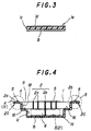
- the metal-base wiring board 1a in this embodiment has a three-layer structure consisting of an aluminum film 1b, polyimide resin 1c and copper foil 1d as shown in Fig. 3. Namely, the polyimide resin 1c is attached between the aluminum film 1b and copper foil 1d.
- the wiring conductors 2 and grounding conductor 3 are formed on the copper foil 1d of the metal-base wiring board 1a as shown in Fig. 2. Therefore, the inner surface of the enclosure member 1 is formed by the wiring conductors 2, grounding conductor 3 and the polyimide resin 1 on which the conductors 2 and 3 are formed, while the entire aluminum film 1b as outer surface of the enclosure member 1 forms an electromagnetic shielding surface.
- the aluminum film 1b as the outer surface is 0.2 mm thick
- the polyimide resin 1c as the intermediate layer is 40 ⁇ m
- the copper foil 1d as the inner surface is 35 ⁇ m.
- the thickness of these layers should preferably be selected so that during forming, by drawing, of the enclosure member 1 into the above-mentioned form of a shallow tray, the polyimide resin 1c and copper foil 1d will not peeled off the aluminum film 1b;
- the insulation layer thickness should range from 20 to 60 ⁇ m, the copper foil thickness range from 18 to 20 ⁇ m and the base metal thickness range from 0.1 to 3.0 mm.
- the aluminum film is used as base metal in view of its drawability, but for a better effect of shielding, a metal of Fe or Cu family should preferably be used for the base metal. Since it needs no rust-proofing treatment, nickel silver should preferably be used. Further, the insulation layer may be made of a resin in an epoxy family in stead of the polyimide family.
- the inner surface of the tray-like enclosure member 1 has a substantially flat bottom 12 on which grounding conductor 3 is formed, a first wall 14 rising from the circumferential edge of the bottom 12, a step 16 contiguous to the first wall 14 and substantially parallel to the bottom 12, a second wall 18 rising from the circumferential edge of the bottom 14, and a circumferential edge 20 continuous to the second wall 18 and substantially parallel to the bottom 14.
- a portion of a concavity 13 defined by the bottom 12, first wall 14, step 16 and second wall 18, that is, a concavity defined by the bottom 12 and second wall 14, has a substantial volume for housing the bare Semiconductor chip 6.
- the level of the step 16 is nearly coincident with the top of the bare semiconductor chip 6 when housed in the enclosure member 1 as joined to the grounding conductor 3.
- Multiple wiring conductors 2a corresponding to the terminal electrodes of the bare semiconductor chip 6 are provided in parallel to each other on the step 16, second wall 18 and circumferential edge 20. Each of these wiring conductors 2a has one end thereof disposed on the step 16 while the other end is disposed on the circumferential edge 20.
- the one end of the wiring conductor 2a on the step 16 is to be electrically connected to the terminal electrode of the bare semiconductor chip 6 by means of a thin wire 6 made of Au or Al by the wire bonding method, while the other end on the circumferential edge 20 is to be electrically connected by soldering to a printed wire (not shown) on a circuit board 9 which will be further discussed later, namely, the bare semiconductor chip 6 is surface-mounted with the face down.
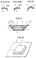
- the bare semiconductor chip 6 and fine wire 7 thus electrically connected are buried in a mold resin 8 by the drip coating method as shown in Fig. 7.
- the step 16 is formed on the inner surface of the enclosure member 1 so that the terminal electrode of the bare semiconductor chip 6 is efficiently electrically connected to the wiring conductor 2a by wire bonding, but the step 16 is unnecessary depending upon the type of the semiconductor chip used.
- the four wiring conductors 2b extending from the grounding conductor 3 formed on the bottom 14 run over the step 16, second wall 18 and circumferential edge 20 and are electrically connected to the aluminum film 1b.
- These ground wiring conductors 2b are so formed on the metal-base wiring board 1a as to have a length over the cutting line indicated with a dash line as shown in Fig. 2.
- the ground wiring conductors 2b pressed and remain as not cut off but as joined to the outer surface of the enclosure member, that is, the aluminum film 1b. This is shown as enlarged in scale in Fig. 5(b). Because of such punching, the wiring for grounding the aluminum film 1b as electromagnetic shield becomes unnecessary.
- a plurality of conductors 2a for connection to the terminal electrodes of the bare semiconductor chip 6 are formed somewhat short of the cutting line so that they do not remain not cut off when the metal-base wiring board 1a is cut. This is shown as enlarged in scale in Fig. 5(a). As shown, the polyimide resin 1c is exposed at the position indicated with 4 to provide a mutual isolation the wiring conductor 2a and the aluminum film 1b forming the outer surface of the enclosure member 1.
- a semiconductor device having a large number of wiring conductors 2a and grounding conductors 2b formed on the circumferential edge 20 of the enclosure member 1 is disposed on printed wires with the opening 13 thereof down to electrically connect the conductors to the printed wires of the circuit board 9 by the reflow soldering process.
- the circumferential edge 20 of the enclosure member 1 has a projection 5 extending in a direction perpendicular to the wiring conductors 2 as shown in Figs. 4 and 5 .
- the wiring conductors 2 are in substantial line contact with the printed wires (not shown) on the circuit board 9 to provide a satisfactory electrical connection between them when the enclosure member 1 is surface-mounted on the circuit board 9 with the face thereof down as shown in Fig. 8.
- the printed wires on the circuit board 9 have a cream solder already applied as printed in positions corresponding to the wiring conductors 2.
- the entire enclosure member 1 disposed on the circuit board 9 is moved for a predetermined time through a heating zone, so that the cream solder is melted, flows toward the surface of the projections 5 on the corresponding wiring conductors and is set there.
- the practical advantage of the projection 5 provided along the circumferential edge of the enclosure member 1 is that it can securely maintain the physical contact between the wiring conductors 2 and printed wires on the circuit board 9 even when the enclosure member 1 is moved in the heating zone and make it easier for an excess melted solder to escape in a direction perpendicular to the extending direction of the projection 5 than in case the surface of contact between the wiring conductors 2 and the printed wires on the circuit board 9 is flat.
- the projection 5 may have formed on the end thereof a smaller projection 5a corresponding to each wiring conductor 2.
- These small projections 5a are substantially semispheric and have a smaller curvature than that of the projection 5, so that the wiring conductor 2 can be in substantial point contact with the printed wire on the circuit board 9.
- the practical advantage of the small projection 5a on the end of the projection 5 can be found in case there are provided a large number of wiring conductors 2 and thus the distance between the adjacent wiring conductors is short, namely the wiring conductors are disposed with a fine pitch.
- the excess melted solder can escape easily in the extending direction of the projection 5 as well as in a direction perpendicular to the extending direction, whereby it is possible to prevent a solder bridge from being formed between the wiring conductors.
- a single enclosure member 1 is formed from a single flat metal-base wiring board 1a.
- a plurality of enclosure members can be formed from a single metal-base wiring board 1a in practice. Namely, a plurality of conductor patterns shown in Fig. 2 is formed as etched on the copper foil 1d of a single metal-base wiring board 1a beforehand, the metal-base wiring board 1a is cut by punching along the dash-line to form a plurality of wiring boards. These wiring boards are drawn into enclosure members each having the form of a shallow tray. Namely, this method assures a high mass-producibility of such enclosure member.
- the enclosure member 1 has formed grounding conductors 3 formed on the bottom 12 thereof. However, it is of course that the grounding conductors 3 are not necessary depending upon the type of the semiconductor chip 6. And many wiring conductors 2 are disposed along the whole circumferential edge of the enclosure member 1. Depending upon the type of the semiconductor chip 6, however, the wiring conductors 2 are disposed along one to three of the four circumferential edges of the enclosure member 1 as the case may be. In this case, grounding conductors 2b may be appropriately disposed on the other circumferential edge or all the other circumferential edges may be formed as grounding conductor in order to enhance the Joining strength and shielding effect when the enclosure member is surface-mounted.
- a bare semiconductor chip is buried in an enclosure member having itself an electromagnetic shield, so that the semiconductor device needs no separate shielding means as in the prior art.
- the packaging density is considerably improved, the number of parts is reduced and manufacturing costs can be noticeably decreased.
- many identical leadless packages can be formed from an extremely thin metal-base wiring board. That is, such leadless packages can be produced with a high mass-producibility. Since the leadless package is so constructed as to be surface-mounted with the face down, the flat bottom thereof conveniently receives a part or parts, so such leadless packages can be automatically transported from one to another station and mechanically mounted on a circuit board.
- the semiconductor device according to the present invention includes a leadless package for base semiconductor chips such as IC, LSI, etc. as well as for thin film elements including thin-film L, C and R elements or combinations of them.
- Figs. 9 to 11 show a second embodiment of the semiconductor device according to the present invention.
- the reference numeral 21 indicates a leadless package or enclosure member which houses a double-sided mounting circuit board 26 on both sides of which a plurality of circuit elements 27 such as semiconductor chips is provided as will be discussed later.
- the enclosure member 21 has an opening 40 of a substantially same size as that of the double-sided mounting circuit board 26.
- the enclosure member 21 is formed by a single thin flat metal-base wiring board 31a having three layers, that is, a nickel silver film 31b, polyimide resin 31c and copper foil 31d (the later structure is not shown).
- the thickness of each layer in this embodiment is as follows.
- the nickel silver film 31b as outer surface is 0.15 mm thick
- the polyimide resin 31c as insulation layer is 20 ⁇ m
- the copper foil 31d as inner surface is 35 ⁇ m.
- the metal-base wiring board is used which has an aluminum film as the base layer since it can be easily drawn, but in this second embodiment, a metal-base wiring board 31a is used which has the nickel silver film 31b as the base layer since it needs no rust-proofing process, is highly elastic and provides a higher shielding effect.
- the insulation resin layer may be made of a resin in an epoxy family in stead of the polyimide family, as in the first embodiment.
- the enclosure member 21 made of such materials is formed by cutting, by punching, a metal-base wiring board 31a along a predetermined development line, bending or drawing into the form of a box.
- the wiring conductors 24 which will be described later are formed as etched beforehand on the copper foil 31d of the metal-base wiring board before bent or drawn.
- the inner surface of the enclosure member 1 is defined by the wiring conductors 24 and the polyimide resin on which the conductors are formed, and the outer surface is defined by the entire nickel silver film 31b to form an electromagnetic shielding surface.
- the wiring conductors 24 include a plurality of circuit connecting conductors 24a and grounding conductors 24b.
- the circuit connecting conductors 24a and grounding conductors 24b have each the one end thereof so disposed inside the enclosure member 21 as to be connected to the terminal electrode formed on the circumferential edge of the double-sided mounting circuit board 26 and which are connected to a circuit element 27 such as semiconductor chip or the like, while the other end is so disposed outside over the opening end of the enclosure member 21 as to be connected to the wiring electrode on the motherboard 30. More particularly, the grounding conductors 24b are extended to outside the enclosure member 21 and connected to the nickel silver film 31b as the outer surface of the enclosure member 21.
- grounding conductors 24b are so formed already on the metal-base wiring board 31a as to have a length over the cutting line. When the metal-base wiring board 31a is cut as punched, the grounding conductors 31a remain as not cut off but as flattened to have an electrical contact with the nickel silver film 31b.
- the enclosure member 21 may have an internal wiring conductor 24c formed on the bottom thereof.
- a circuit element 28 may be disposed inside the enclosure member 21 as well as on the double-sided mounting circuit board 26 as shown in Fig. 12.
- the internal wiring conductor 24c may be so formed as to connect the circuit element 28 to the terminal electrodes of the double-sided mounting circuit board 26, or it may be so extended to outside over the opening end of the enclosure member 21 as to be connected to the wiring electrodes on the motherboard 30.
- the enclosure member 21 has formed on the lateral wall thereof a plurality of projections 23 which are used to position the double-sided mounting circuit board 26 in place inside the enclosure member 21.
- each lateral wall has formed thereon two projections 23a which engage on the upper surface of the double-sided mounting circuit board 26 and two projections 23b which engage the rear surface of the double-sided mounting circuit board 26.
- the double-sided mounting circuit board 26 is inserted from the opening 40 and fixed as fitted between the projections 23a and 23b. Since the enclosure member 21 is made from a metal-base wiring board 31a having the nickel silver film 31b as the base layer, the double-sided mounting circuit board 26 can be easily fitted between the projections 23a and 23b.
- the circumferential end face of the double-sided mounting circuit board 26 abuts the lateral wall of the enclosure member 21 so that the upper and rear surfaces of the latter will be blocked by the plurality of projections 23a and 23b from being moved up and down.
- the terminal electrodes formed on the circumferential edge of the double-sided mounting circuit board 26 fitted between the projections 23a and 23b, and connected to the circuit element 27 such as semiconductor chip or the like, are in contact and connected as soldered with the ends, respectively, of the circuit connecting conductors 24a.
- the opening end of the enclosure member 1 is bent outwardly and over the outer surface thereof as shown in Fig. 11 to form a bend 22 having a U-shaped section.
- the wiring conductors 24 including the circuit connecting conductors 24a are extended outwardly from inside the enclosure member 21 through the bend 22.
- the wiring conductors 24 are in substantially line contact with the wiring electrodes on the motherboard 30 along the bending line of the bend 22 and soldered as they are to the wiring electrodes on the motherboard 30.
- This soldering may be done by the reflow soldering process as in the first embodiment, whereby a satisfactory physical contact and electrical connection can be assured between the wiring conductors 24 and the wiring electrodes on the motherboard 30.
- a small projection may be formed in a position along the bending line of the bend 22 correspondingly to each wiring conductor 24. These small projections have a smaller curvature than the bend 22 has and the wiring conductors 24 can have substantial point contact with the printed wires on the motherboard 30.
- the practical advantage of such small projections provided in positions along the bending line of the bend 22 lies in that the plurality of wiring conductors 24 are disposed with a fine pitch and it is possible for the excess melted solder to escape in a direction along the bending line of the bend 22 as well as in a direction perpendicular to that direction, thereby permitting to block a solder bridge from being formed between the wiring conductors 24.
- a double-sided mounting circuit board and electronic parts can be fixed as closely packed within the box-shaped enclosure member having itself an electromagnetic shield and the enclosure member itself can be surface-mounted on the motherboard.
- Such fixation and surface-mounting can be done by the reflow soldering process. Therefore, the assembling time can be considerably reduced and thus manufacturing costs can be decreased.
- the box-shaped enclosure members can be formed from a single thin, flat metal-base wiring board and not only the double-sided mounting circuit board but also other electronic parts can be disposed as closely packed inside the enclosure member, the packaging density is considerably improved.
Landscapes
- Engineering & Computer Science (AREA)
- Microelectronics & Electronic Packaging (AREA)
- Shielding Devices Or Components To Electric Or Magnetic Fields (AREA)
Applications Claiming Priority (4)
| Application Number | Priority Date | Filing Date | Title |
|---|---|---|---|
| JP85864/91 | 1991-03-27 | ||
| JP85865/91 | 1991-03-27 | ||
| JP3085864A JP2952286B2 (ja) | 1991-03-27 | 1991-03-27 | ベアチップリードレスパッケージ |
| JP3085865A JP2598344B2 (ja) | 1991-03-27 | 1991-03-27 | 両面実装基板用リードレスパッケージケース |
Publications (3)
| Publication Number | Publication Date |
|---|---|
| EP0506090A2 true EP0506090A2 (de) | 1992-09-30 |
| EP0506090A3 EP0506090A3 (en) | 1993-05-26 |
| EP0506090B1 EP0506090B1 (de) | 1997-01-08 |
Family
ID=26426866
Family Applications (1)
| Application Number | Title | Priority Date | Filing Date |
|---|---|---|---|
| EP92105319A Expired - Lifetime EP0506090B1 (de) | 1991-03-27 | 1992-03-27 | Halbleiteranordnung mit elektromagnetischer Abschirmung |
Country Status (3)
| Country | Link |
|---|---|
| US (1) | US5352925A (de) |
| EP (1) | EP0506090B1 (de) |
| DE (1) | DE69216452T2 (de) |
Cited By (3)
| Publication number | Priority date | Publication date | Assignee | Title |
|---|---|---|---|---|
| US6509629B2 (en) * | 2000-08-24 | 2003-01-21 | Mitsubishi Denki Kabushiki Kaisha | Power module |
| US6691296B1 (en) * | 1998-02-02 | 2004-02-10 | Matsushita Electric Industrial Co., Ltd. | Circuit board design aiding |
| CN106252339A (zh) * | 2016-08-11 | 2016-12-21 | 国网辽宁省电力有限公司电力科学研究院 | 一种高密度射频多芯片封装结构 |
Families Citing this family (18)
| Publication number | Priority date | Publication date | Assignee | Title |
|---|---|---|---|---|
| US5639990A (en) * | 1992-06-05 | 1997-06-17 | Mitsui Toatsu Chemicals, Inc. | Solid printed substrate and electronic circuit package using the same |
| US5869889A (en) * | 1997-04-21 | 1999-02-09 | Lsi Logic Corporation | Thin power tape ball grid array package |
| US6288344B1 (en) * | 1999-08-20 | 2001-09-11 | Cardiac Pacemakers, Inc. | Integrated EMI shield utilizing a hybrid edge |
| US6717241B1 (en) * | 2000-08-31 | 2004-04-06 | Micron Technology, Inc. | Magnetic shielding for integrated circuits |
| DE10102119C1 (de) * | 2001-01-18 | 2002-04-04 | Vishay Semiconductor Gmbh | Optoelektronisches Bauelement mit Leiterstreifenaufbau und Verfahren zu seiner Herstellung |
| DE10146854B4 (de) * | 2001-09-24 | 2009-05-20 | Infineon Technologies Ag | Elektronisches Bauteil mit wenigstens einem Halbleiterchip und Verfahren zur Herstellung eines elektronischen Bauteils mit wenigstens einem Halbleiterchip |
| US6834791B2 (en) * | 2002-01-24 | 2004-12-28 | Nas Interplex Inc. | Solder-bearing components and method of retaining a solder mass therein |
| WO2003061894A1 (en) * | 2002-01-24 | 2003-07-31 | Interplex Nas, Inc. | Solder-bearing components including a solder-bearing electromagnetic shield and method of retaining a solder mass therein |
| US6796485B2 (en) * | 2002-01-24 | 2004-09-28 | Nas Interplex Inc. | Solder-bearing electromagnetic shield |
| US20070119620A1 (en) * | 2005-11-29 | 2007-05-31 | Rodriguez Jose F | Flexible circuit shields |
| TWI409924B (zh) * | 2007-09-12 | 2013-09-21 | 日月光半導體製造股份有限公司 | 半導體封裝體及其製造方法 |
| CN102378565A (zh) * | 2010-08-19 | 2012-03-14 | 环旭电子股份有限公司 | 盖体及使用该盖体的电子装置 |
| JP2012069764A (ja) | 2010-09-24 | 2012-04-05 | On Semiconductor Trading Ltd | 回路装置およびその製造方法 |
| KR101330770B1 (ko) * | 2011-11-16 | 2013-11-18 | 엘지이노텍 주식회사 | 백라이트 유닛용 절곡 인쇄회로기판 |
| US9250651B2 (en) | 2013-04-24 | 2016-02-02 | Google Technology Holdings LLC | Electronic device with folded display |
| TWI690043B (zh) * | 2016-02-17 | 2020-04-01 | 瑞昱半導體股份有限公司 | 積體電路裝置 |
| JP6815880B2 (ja) * | 2017-01-25 | 2021-01-20 | 株式会社ディスコ | 半導体パッケージの製造方法 |
| KR102822198B1 (ko) * | 2020-04-17 | 2025-06-18 | 삼성전자주식회사 | 쉴드 캔을 포함하는 전자 장치 |
Family Cites Families (4)
| Publication number | Priority date | Publication date | Assignee | Title |
|---|---|---|---|---|
| US4147889A (en) * | 1978-02-28 | 1979-04-03 | Amp Incorporated | Chip carrier |
| US4551746A (en) * | 1982-10-05 | 1985-11-05 | Mayo Foundation | Leadless chip carrier apparatus providing an improved transmission line environment and improved heat dissipation |
| JPS6445134A (en) * | 1987-08-14 | 1989-02-17 | Hitachi Ltd | Semiconductor device |
| JPH03120746A (ja) * | 1989-10-03 | 1991-05-22 | Matsushita Electric Ind Co Ltd | 半導体素子パッケージおよび半導体素子パッケージ搭載配線回路基板 |
-
1992
- 1992-03-26 US US07/857,420 patent/US5352925A/en not_active Expired - Fee Related
- 1992-03-27 DE DE69216452T patent/DE69216452T2/de not_active Expired - Fee Related
- 1992-03-27 EP EP92105319A patent/EP0506090B1/de not_active Expired - Lifetime
Cited By (4)
| Publication number | Priority date | Publication date | Assignee | Title |
|---|---|---|---|---|
| US6691296B1 (en) * | 1998-02-02 | 2004-02-10 | Matsushita Electric Industrial Co., Ltd. | Circuit board design aiding |
| US6509629B2 (en) * | 2000-08-24 | 2003-01-21 | Mitsubishi Denki Kabushiki Kaisha | Power module |
| CN106252339A (zh) * | 2016-08-11 | 2016-12-21 | 国网辽宁省电力有限公司电力科学研究院 | 一种高密度射频多芯片封装结构 |
| CN106252339B (zh) * | 2016-08-11 | 2019-01-25 | 国网辽宁省电力有限公司电力科学研究院 | 一种高密度射频多芯片封装结构 |
Also Published As
| Publication number | Publication date |
|---|---|
| DE69216452D1 (de) | 1997-02-20 |
| EP0506090B1 (de) | 1997-01-08 |
| EP0506090A3 (en) | 1993-05-26 |
| US5352925A (en) | 1994-10-04 |
| DE69216452T2 (de) | 1997-07-31 |
Similar Documents
| Publication | Publication Date | Title |
|---|---|---|
| US5352925A (en) | Semiconductor device with electromagnetic shield | |
| KR960003766B1 (ko) | 플래스틱 핀 그리드 어레이 패키지 제조 방법 | |
| EP0720232B1 (de) | Viel-chip-modul | |
| US4819041A (en) | Surface mounted integrated circuit chip package and method for making same | |
| EP0004148A1 (de) | Elektrisches Verbindungsstück zur Montage einer elektronischen Vorrichtung auf ein Substrat | |
| EP0001892A1 (de) | Leitergitter und Gehäuse zum Herstellen von elektrischen Anschlüssen an elektronischen Bauelementen | |
| US20040232452A1 (en) | Module component | |
| US4668032A (en) | Flexible solder socket for connecting leadless integrated circuit packages to a printed circuit board | |
| EP0330372A2 (de) | Integrierte Hybridschaltung mit Wärmesenke | |
| US6847115B2 (en) | Packaged semiconductor device for radio frequency shielding | |
| US5455741A (en) | Wire-lead through hole interconnect device | |
| US6329594B1 (en) | Integrated circuit package | |
| US5596171A (en) | Package for a high frequency semiconductor device and methods for fabricating and connecting the same to an external circuit | |
| US6320762B1 (en) | Fixed conductive pin for printed wiring substrate electronics case and method of manufacture therefor | |
| US5665649A (en) | Process for forming a semiconductor device base array and mounting semiconductor devices thereon | |
| CN118352850A (zh) | 一种光学驱动组件及其制造方法 | |
| CN111613598A (zh) | 具有集成emi屏蔽的半导体装置 | |
| US6717822B1 (en) | Lead-frame method and circuit module assembly including edge stiffener | |
| US4611092A (en) | Surface mount package for toroids | |
| JP2598344B2 (ja) | 両面実装基板用リードレスパッケージケース | |
| WO1996030943A1 (en) | Thin profile integrated circuit package | |
| EP4513548A1 (de) | Elektronisches bauelement und anordnung | |
| JPH1197820A (ja) | 電磁シールド用導体パターンが形成された回路基板 | |
| JPH07221427A (ja) | 表面実装用パッケージ及びパッケージ実装装置 | |
| GB2265760A (en) | Electromagnetically shielding printed circuit boards |
Legal Events
| Date | Code | Title | Description |
|---|---|---|---|
| PUAI | Public reference made under article 153(3) epc to a published international application that has entered the european phase |
Free format text: ORIGINAL CODE: 0009012 |
|
| AK | Designated contracting states |
Kind code of ref document: A2 Designated state(s): DE FR GB |
|
| PUAL | Search report despatched |
Free format text: ORIGINAL CODE: 0009013 |
|
| AK | Designated contracting states |
Kind code of ref document: A3 Designated state(s): DE FR GB |
|
| 17P | Request for examination filed |
Effective date: 19931125 |
|
| 17Q | First examination report despatched |
Effective date: 19950215 |
|
| GRAG | Despatch of communication of intention to grant |
Free format text: ORIGINAL CODE: EPIDOS AGRA |
|
| GRAH | Despatch of communication of intention to grant a patent |
Free format text: ORIGINAL CODE: EPIDOS IGRA |
|
| RAP1 | Party data changed (applicant data changed or rights of an application transferred) |
Owner name: GOYO ELECTRONICS CO., LTD. Owner name: KOKUSAI ELECTRIC CO., LTD. |
|
| GRAH | Despatch of communication of intention to grant a patent |
Free format text: ORIGINAL CODE: EPIDOS IGRA |
|
| GRAA | (expected) grant |
Free format text: ORIGINAL CODE: 0009210 |
|
| AK | Designated contracting states |
Kind code of ref document: B1 Designated state(s): DE FR GB |
|
| REF | Corresponds to: |
Ref document number: 69216452 Country of ref document: DE Date of ref document: 19970220 |
|
| ET | Fr: translation filed | ||
| PLBE | No opposition filed within time limit |
Free format text: ORIGINAL CODE: 0009261 |
|
| STAA | Information on the status of an ep patent application or granted ep patent |
Free format text: STATUS: NO OPPOSITION FILED WITHIN TIME LIMIT |
|
| 26N | No opposition filed | ||
| REG | Reference to a national code |
Ref country code: FR Ref legal event code: CD Ref country code: FR Ref legal event code: CA |
|
| REG | Reference to a national code |
Ref country code: FR Ref legal event code: CD Ref country code: FR Ref legal event code: CA |
|
| REG | Reference to a national code |
Ref country code: GB Ref legal event code: IF02 |
|
| PGFP | Annual fee paid to national office [announced via postgrant information from national office to epo] |
Ref country code: GB Payment date: 20041229 Year of fee payment: 14 Ref country code: DE Payment date: 20041229 Year of fee payment: 14 |
|
| PGFP | Annual fee paid to national office [announced via postgrant information from national office to epo] |
Ref country code: FR Payment date: 20050324 Year of fee payment: 14 |
|
| PG25 | Lapsed in a contracting state [announced via postgrant information from national office to epo] |
Ref country code: GB Free format text: LAPSE BECAUSE OF NON-PAYMENT OF DUE FEES Effective date: 20060327 |
|
| PG25 | Lapsed in a contracting state [announced via postgrant information from national office to epo] |
Ref country code: DE Free format text: LAPSE BECAUSE OF NON-PAYMENT OF DUE FEES Effective date: 20061003 |
|
| GBPC | Gb: european patent ceased through non-payment of renewal fee |
Effective date: 20060327 |
|
| REG | Reference to a national code |
Ref country code: FR Ref legal event code: ST Effective date: 20061130 |
|
| PG25 | Lapsed in a contracting state [announced via postgrant information from national office to epo] |
Ref country code: FR Free format text: LAPSE BECAUSE OF NON-PAYMENT OF DUE FEES Effective date: 20060331 |