EP0504882A2 - Optisches Wellenleiterbauelement und Verfahren für dessen Verbindung mit einer optischen Faser - Google Patents
Optisches Wellenleiterbauelement und Verfahren für dessen Verbindung mit einer optischen Faser Download PDFInfo
- Publication number
- EP0504882A2 EP0504882A2 EP92104790A EP92104790A EP0504882A2 EP 0504882 A2 EP0504882 A2 EP 0504882A2 EP 92104790 A EP92104790 A EP 92104790A EP 92104790 A EP92104790 A EP 92104790A EP 0504882 A2 EP0504882 A2 EP 0504882A2
- Authority
- EP
- European Patent Office
- Prior art keywords
- cladding
- optical waveguide
- core
- waveguide device
- optical
- Prior art date
- Legal status (The legal status is an assumption and is not a legal conclusion. Google has not performed a legal analysis and makes no representation as to the accuracy of the status listed.)
- Withdrawn
Links
Images


Classifications
-
- G—PHYSICS
- G02—OPTICS
- G02B—OPTICAL ELEMENTS, SYSTEMS OR APPARATUS
- G02B6/00—Light guides; Structural details of arrangements comprising light guides and other optical elements, e.g. couplings
- G02B6/24—Coupling light guides
- G02B6/26—Optical coupling means
- G02B6/30—Optical coupling means for use between fibre and thin-film device
-
- G—PHYSICS
- G02—OPTICS
- G02B—OPTICAL ELEMENTS, SYSTEMS OR APPARATUS
- G02B6/00—Light guides; Structural details of arrangements comprising light guides and other optical elements, e.g. couplings
- G02B6/10—Light guides; Structural details of arrangements comprising light guides and other optical elements, e.g. couplings of the optical waveguide type
- G02B6/12—Light guides; Structural details of arrangements comprising light guides and other optical elements, e.g. couplings of the optical waveguide type of the integrated circuit kind
- G02B6/122—Basic optical elements, e.g. light-guiding paths
-
- G—PHYSICS
- G02—OPTICS
- G02B—OPTICAL ELEMENTS, SYSTEMS OR APPARATUS
- G02B6/00—Light guides; Structural details of arrangements comprising light guides and other optical elements, e.g. couplings
- G02B6/24—Coupling light guides
- G02B6/42—Coupling light guides with opto-electronic elements
- G02B6/4201—Packages, e.g. shape, construction, internal or external details
- G02B6/4249—Packages, e.g. shape, construction, internal or external details comprising arrays of active devices and fibres
Definitions
- the present invention relates to an optical waveguide device and a method for connecting an optical waveguide and an optical fiber using the optical waveguide device.
- optical waveguide device In the field of optical communication or optical transmission, various optical devices such as optical switches and optical couplers are used in addition to optical transmitters, optical receivers, and optical transmission lines.
- optical waveguide device As one of the types of such optical devices, there is an optical waveguide device.
- the optical waveguide device is arranged in such a way that an optical waveguide is formed on a substrate and a light beam is controlled while it is confined in the optical waveguide. Because of its structure, the optical waveguide device has such advantages that it can be easily miniaturized and produced on a mass scale using the planar technique and, in addition, that electric field or magnetic field can be applied thereto effectively.
- an object of the present invention is to provide an optical waveguide device which can be easily connected with an optical fiber.
- Another object of the present invention is to provide a method for easily connecting an optical waveguide and an optical fiber using the optical waveguide device.
- an optical waveguide device comprising a substrate having a top surface, a first cladding with a uniform thickness formed on the substrate, a core formed on the first cladding, a recognizable thin layer formed on the first cladding on both sides of the core, the thin layer defining a reference plane which is parallel to the top surface of the substrate and lies substantially in the same plane as the bottom surface of the core, and a second cladding formed on the first cladding so as to cover the core.
- an optical waveguide device comprising a substrate having a top surface, a first cladding with a uniform thickness formed on the substrate, a core formed on the first cladding, a reference layer with the same thickness as the core formed on the first cladding on both sides of the core, the reference layer defining a reference plane lying in the same plane as the top surface of the core, and a second cladding formed on the first cladding so as to cover the core.
- the connection of the optical waveguide device with an optical fiber can be achieved by bringing the reference plane into contact with a plane which is in a predetermined relative position to the optical fiber and making only a planar positioning adjustment.
- the connection of the optical waveguide device with the optical fiber can be achieved using smaller man-hours than positional adjustment than in the conventional connecting method.
- the present invention by providing a plane in a predetermined relative position to an optical fiber to which the optical waveguide device is to be connected, makes it possible to make positioning adjustment only by planar sliding between the plane and the reference plane and achieve the connection between the optical fiber and the optical waveguide device with a high optical coupling efficiency.
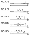
- a manufacturing process of an optical waveguide device of an embodiment of the present invention will be described.
- a first cladding 4 having SiO2 as its main component and having a relatively low refractive index is formed with a uniform thickness on a substrate 2 of Si for example by a CVD method and a visually recognizable Si thin film layer 6, which defines a reference plane, is formed on the first cladding 4 at its opposite edge portions.
- a core layer 8 having a higher refractive index than the first cladding 4 is formed on the first cladding 4 and Si thin film layer 6 and, on the core layer 8, Si patterns 10 in a shape corresponding to the shape of cores to be produced are formed.
- the core layer 8 can be formed of SiO2 doped with germanium or titanium.
- the portion of the core layer 8 where the Si patterns 10 are not formed is removed by etching, whereby a plurality of cores 8a of a predetermined shape are produced as show in FIG. 1(C), and then, a second cladding 12, of the same quality as the first cladding 4, is formed on the first cladding 4 so as to cover the cores 8a. Since the visually recognizable Si thin film layer 6 is formed on the first cladding 4, the etching of the core layer 8 can be stopped when the core layer is removed to the level of the Si thin film layer 6. If the Si thin film layer 6 were not formed, because the first cladding 4 and the core layer 8 are transparent, it would be very difficult to stop etching of the core layer 8 at the desired position.
- the Si thin film layer 6 being approximately 0.1 - 0.3 ⁇ m thick, is very thin, its top surface is virtually lies in the same plane as the bottom surface of the cores 8a. After the etching of the core layer 8 has been finished, the Si patterns 10 remaining on the cores 8a are removed.
- a mask 14 is formed on the second cladding 12 so as to cover the cores 8a and the exposed portion of the second cladding 12 is removed by etching.
- that portion of the second cladding 12 is removed and as a result the Si thin film layer 6 defining the reference plane appears uncovered on both sides of the cores 8a.
- the Si thin film layer 6 defining the reference plane can be formed lying virtually in the same plane as the bottom surfaces of the cores 8a, the positioning adjustments between the cores 8a and optical fibers can be achieved easily and reliably by using the reference plane as described later in detail.
- the cladding covering cores (the second cladding in the present embodiment) is 10 to 20 ⁇ m thick and this thickness is liable to fluctuate according to manufacturing conditions. Therefore, it is not advantageous to use the top surface of the second cladding 12 as the reference plane. In order to secure highly precise relative position between the reference plane and the core, it is preferable to form the reference plane on the first cladding 4 as in this embodiment.
- the visually recognizable reference plane was formed on the first cladding 4, it is also practicable, when etching the core layer 8, to leave portions of the core layer 8 on both sides of the cores 8a unetched and use the top surface of the core layer 8 thus left unetched as the reference plane.
- the reference plane is lying in the same plane as the top surfaces of the cores 8a, and thus, the same as in the above described embodiment, highly precise relative position between the reference plane and the cores 8a can be secured.
- FIG. 2 a method for connecting an optical waveguide with an optical fiber using the optical waveguide device 16 manufactured in the manufacturing process of FIG. 1 will be described.
- a rectangular opening 20 capable of receiving the second cladding 12 of the optical waveguide device 16.
- V grooves 22a and 22b are formed between the end faces in the lengthwise direction of the substrate 18 and the wall surfaces of the opening 20, in parallel, for receiving the optical fibers 28 to be connected.
- the pitch between the V grooves 22a and 22b is the same as the pitch between the cores 8a of the optical waveguide device 16.
- the respective V grooves 22a are aligned with the respective V grooves 22b.
- the substrate 18 further has two V grooves 24 provided on both sides of the opening 20 extending between both end faces of the substrate in its lengthwise direction.
- the V grooves 24 are virtually parallel to each other and the V grooves 24 are also virtually parallel to the V grooves 22a and 22b, but they need not be precisely parallel.
- Reference numeral 26 denotes a columnar rod partly received in the V groove 24.
- the V groove 24 is formed deeper than the V grooves 22a and 22b and the columnar rod 26 is larger in diameter than the optical fiber 28.
- the optical fibers 28, and the columnar rods 26 are seated in the V grooves 22a and 22b, and 24, respectively, of the substrate 18 and, then, the optical waveguide device 16 is mounted on the substrate 18 in such a way that the Si thin film layer 6 defining the reference plane of the optical waveguide device 16 comes into contact with the columnar rods 26.
- the shapes of the V grooves 22a, 22b, and 24 and the diameters of the optical fibers 28 and the columnar rods 26 are set so that each core 8a of the waveguide and the core of the optical fiber 28 are lying in the same plane at this time.
- the optical fiber 28 can be brought into alignment with the core 8a of the waveguide by adjusting the optical waveguide device 16 only in a plane parallel to the surface of the substrate 18, and hence the connection work is quite easy.
- the positioning adjustment of the optical waveguide device 16 relative to the optical fiber 28 is carried out, by introducing a laser beam into the optical fiber 28 received in the V groove 22a and connecting the optical fiber received in the V groove 22b to an optical power meter, so that the maximum optical coupling efficiency may be obtained.
- the optical waveguide device 16 and the optical fiber 28 are fixed to the substrate 18 with a boding agent.
- the V grooves 22a, 22b, and 24 can be formed with high precision for example by anisotropic etching of silicon.
- the relative position between the reference plane and the core 8a of the waveguide can be set up with high precision. Therefore, once the end face of one of the cores 8a of the optical waveguide device 16 has been connected with the optical fiber 28, another optical fiber 28 to be connected to the other core can be brought into accurate confrontation with the core 8a by pushing the optical fiber against the end face of the waveguide along the V groove 22a.
- the substrate 18 together with the columnar rods 26 may be cut into two laterally around the center in the longitudinal direction, and connection of the optical waveguide device and the optical fiber may be made using each of the divided parts.
- the positioning adjustments of the divided optical waveguide devices with respect to the optical fibers must be made for both end faces in the lengthwise direction of the divided optical waveguide devices 16 individually.
- FIG. 3 a method for connecting optical fibers and optical waveguides according to another embodiment of the present invention will be described.
- a substrate 30 made of stainless steel two each of tube ferrules 32 similarly made of stainless steel, in contact with each other, are fixed on the input side and the output side of the optical waveguide device, respectively.
- the ferrules 32 on the input side are aligned with their corresponding ferrules 32 on the output side.
- An optical fiber 28 is placed in and fixed to each of small central holes of the ferrules 32.
- the ferrules 32 and the columnar rods 34 are fixed to the substrate 30 for example by laser welding.
- the optical waveguide device 16 is mounted on the columnar rods 34, and then, only by giving a planar movement to the optical waveguide device 16, that is, by sliding the reference plane of the optical waveguide device 16 along the plane on the columnar rods 34, the positioning adjustment between the cores 8a of the optical waveguide device and the cores of the optical fibers 28 can be achieved easily.
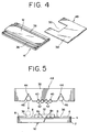
- FIG. 4 and FIG. 5 a method for connecting an optical waveguide device and optical fibers according to a further embodiment of the present invention will be described.
- an optical waveguide device 16' having its reference plane on the top surface of the core layer 8 is used.
- the core layer 8 there are formed two grooves 36 on both sides of the cores 8a.
- Reference numeral 48 denotes a fiber array assembly with a plurality of optical fibers 42 fixed in V grooves 40 formed in a plate 38.
- the plate 38 there are formed two V grooves 44 on both sides of the optical fibers 42.
- a columnar rod 46 is partially received.
- the pitch between the V grooves 40 and the pitch between the cores 8a of the optical waveguide device 16' are equal and the distance between the V grooves 44 and the distance between the grooves 36 are equal.
- At one end portion of the plate 38 there is formed a rectangular cutting 50 and the end faces of the optical fibers 42 are all terminated at the surface of the wall extending in the lateral direction of the walls defining the cutting 50.
- the fiber array assembly 48 is mounted on the optical waveguide device 16' with the columnar rods 46 interposed between the V grooves 44 and the grooves 36.
- the width of the groove 36, the shapes of the V grooves 40 and 44, and the diameters of the optical fiber 42 and the columnar rods 46 are set up so that the cores of the optical fibers 42 and the cores 8a of the optical waveguide device lie in the same plane at this time.
- the end faces of the cores of the optical fibers 42 and the end faces of the cores 8a of the optical waveguide device 16' can be brought into confrontation and contact with each other.
- a bonding agent By fixing the fiber array assembly 48 to the optical waveguide device 16' in this state with a bonding agent, permanent connections between the optical fibers and the cores of the optical waveguides can be realized.
- the optical fiber array and the optical waveguide device can be connected without the need for adjustment.
- the present invention was applied to a quartz type optical waveguide, but the present invention is not limited to that. It can also be applied to an optical waveguide device formed of a plastic material such as polymethyl methacrylate.
Landscapes
- Physics & Mathematics (AREA)
- General Physics & Mathematics (AREA)
- Optics & Photonics (AREA)
- Engineering & Computer Science (AREA)
- Microelectronics & Electronic Packaging (AREA)
- Optical Couplings Of Light Guides (AREA)
- Mechanical Coupling Of Light Guides (AREA)
- Optical Integrated Circuits (AREA)
Applications Claiming Priority (2)
| Application Number | Priority Date | Filing Date | Title |
|---|---|---|---|
| JP78268/91 | 1991-03-19 | ||
| JP3078268A JPH04291205A (ja) | 1991-03-19 | 1991-03-19 | 導波路型光デバイス |
Publications (2)
| Publication Number | Publication Date |
|---|---|
| EP0504882A2 true EP0504882A2 (de) | 1992-09-23 |
| EP0504882A3 EP0504882A3 (en) | 1993-10-27 |
Family
ID=13657236
Family Applications (1)
| Application Number | Title | Priority Date | Filing Date |
|---|---|---|---|
| EP19920104790 Withdrawn EP0504882A3 (en) | 1991-03-19 | 1992-03-19 | Optical waveguide device and method for connecting optical waveguide and optical fiber using the optical waveguide device |
Country Status (4)
| Country | Link |
|---|---|
| US (1) | US5218663A (de) |
| EP (1) | EP0504882A3 (de) |
| JP (1) | JPH04291205A (de) |
| CA (1) | CA2063310A1 (de) |
Cited By (10)
| Publication number | Priority date | Publication date | Assignee | Title |
|---|---|---|---|---|
| GB2293248A (en) * | 1994-09-07 | 1996-03-20 | Northern Telecom Ltd | Optical waveguide component coupling using mating substrates |
| FR2727768A1 (fr) * | 1994-12-05 | 1996-06-07 | Alcatel Nv | Procede pour former une couche de silice a eliminer ulterieurement et procede pour rapporter un composant en optique integree |
| US5611014A (en) * | 1994-12-07 | 1997-03-11 | Lucent Technologies Inc. | Optoelectronic device connecting techniques |
| US5656120A (en) * | 1994-07-28 | 1997-08-12 | Ngk Insulators, Ltd. | Method of fixing optical fiber array to substrate |
| WO1998012585A1 (en) * | 1996-09-17 | 1998-03-26 | Telefonaktiebolaget Lm Ericsson (Publ) | Method for manufacturing an optoelectrical component and an optoelectrical component manufactured according to the method |
| FR2773222A1 (fr) * | 1997-12-31 | 1999-07-02 | Samsung Electronics Co Ltd | Structure pour connecter des fibres optiques a un guide d'onde optique |
| FR2799553A1 (fr) * | 1999-10-12 | 2001-04-13 | France Telecom | Ajustement de l'assemblage d'un composant optique miniature forme par report d'une puce de circuit integre optique sur une plate-forme de connexion de fibres optiques |
| GB2374156A (en) * | 2001-04-02 | 2002-10-09 | Kamelian Ltd | Aligning array of optical fibres with waveguides of optical device |
| US6728450B2 (en) | 2001-04-02 | 2004-04-27 | Kamelian Limited, A Body Corporate | Alignment of optical fibers with an optical device |
| US9939579B2 (en) * | 2000-10-26 | 2018-04-10 | Neophotonics Corporation | Multilayered optical structures |
Families Citing this family (26)
| Publication number | Priority date | Publication date | Assignee | Title |
|---|---|---|---|---|
| US5412748A (en) * | 1992-12-04 | 1995-05-02 | Kabushiki Kaisha Toshiba | Optical semiconductor module |
| US5343544A (en) * | 1993-07-02 | 1994-08-30 | Minnesota Mining And Manufacturing Company | Integrated optical fiber coupler and method of making same |
| US5367593A (en) * | 1993-09-03 | 1994-11-22 | Motorola, Inc. | Optical/electrical connector and method of fabrication |
| US5511138A (en) * | 1994-06-27 | 1996-04-23 | Motorola | Interlocking waveguide and method of making |
| TW281731B (de) * | 1994-08-26 | 1996-07-21 | Akzo Nobel Nv | |
| SE514116C2 (sv) | 1994-10-19 | 2001-01-08 | Ericsson Telefon Ab L M | Förfarande för framställning av en kapslad optokomponent, gjutform för kapsling av en optokomponent och tryckanordning för gjutform |
| JPH09113767A (ja) * | 1995-09-29 | 1997-05-02 | Motorola Inc | 光伝送構造を整合するための電子部品 |
| US5659648A (en) * | 1995-09-29 | 1997-08-19 | Motorola, Inc. | Polyimide optical waveguide having electrical conductivity |
| DE19700549A1 (de) * | 1997-01-10 | 1998-07-16 | Alsthom Cge Alcatel | Vorrichtung zur präzisen Anordnung von mikrooptischen Bauteilen auf einem Träger |
| US6754428B1 (en) * | 2001-03-14 | 2004-06-22 | Zygo Corporation | Fiber array alignment substrate |
| US6744953B2 (en) * | 2001-09-07 | 2004-06-01 | Agilent Technologies, Inc. | Planar optical waveguide with alignment structure |
| US7295742B2 (en) * | 2002-05-31 | 2007-11-13 | Matsushita Electric Industrial Co., Ltd. | Optical element and method for producing the same |
| JP2005128419A (ja) * | 2003-10-27 | 2005-05-19 | Nec Corp | 光導波路構造およびその作製方法 |
| KR100584115B1 (ko) | 2003-12-24 | 2006-05-30 | 전자부품연구원 | 광 스플리터 및 그의 제조방법 |
| USD611628S1 (en) * | 2006-06-20 | 2010-03-09 | Panasonic Corporation | Lighting apparatus |
| US7447405B1 (en) * | 2006-10-23 | 2008-11-04 | International Business Machines Corporation | Ferrule for optical wave guide |
| USD586764S1 (en) * | 2007-02-09 | 2009-02-17 | Panasonic Corporation | Light source of light-emitting diode |
| USD580889S1 (en) * | 2007-02-09 | 2008-11-18 | Panasonic Corporation | Light source of light-emitting diode |
| USD580377S1 (en) * | 2007-02-09 | 2008-11-11 | Panasonic Corporation | Light source of light-emitting diode |
| USD580890S1 (en) * | 2007-02-09 | 2008-11-18 | Panasonic Corporation | Light source of light-emitting diode |
| US10620377B1 (en) * | 2015-04-01 | 2020-04-14 | National Technology & Engineering Solutions Of Sandia, Llc | Kinematic chip to chip bonding |
| JP6467339B2 (ja) * | 2015-12-22 | 2019-02-13 | 日本電信電話株式会社 | 光信号処理装置 |
| US10048455B2 (en) * | 2016-01-18 | 2018-08-14 | Cisco Technology, Inc. | Passive fiber array connector alignment to photonic chip |
| USD825148S1 (en) * | 2016-06-08 | 2018-08-14 | Troy Horning | Clothing accessory to prevent slippage |
| US10288812B1 (en) * | 2018-03-12 | 2019-05-14 | Corning Incorporated | Fiber optic-to-waveguide coupling assembly with overlap for edge coupling |
| US10656339B2 (en) | 2018-03-14 | 2020-05-19 | Cisco Technology, Inc. | Fiber to chip alignment using passive vgroove structures |
Family Cites Families (7)
| Publication number | Priority date | Publication date | Assignee | Title |
|---|---|---|---|---|
| FR2596529B1 (fr) * | 1986-03-28 | 1988-05-13 | Thomson Csf | Guide d'onde optique en materiau semiconducteur, laser appliquant ce guide d'onde et procede de realisation |
| JPS63311212A (ja) * | 1987-06-12 | 1988-12-20 | Sumitomo Electric Ind Ltd | 光導波路装置と、光導波路の実装方法 |
| JPS63316009A (ja) * | 1987-06-19 | 1988-12-23 | Nec Corp | 光結合構造 |
| FR2623915B1 (fr) * | 1987-11-26 | 1990-04-13 | Corning Glass Works | Procede de production d'un composant optique integre en verre comprenant des tranchees de positionnement et de fixation de fibres optiques en alignement avec des guides d'ondes et composants ainsi produits |
| JPH01234806A (ja) * | 1988-03-16 | 1989-09-20 | Sumitomo Electric Ind Ltd | 光導波路装置 |
| FR2658307A1 (fr) * | 1990-02-13 | 1991-08-16 | Thomson Csf | Guide d'onde optique integre et procede de realisation. |
| US5119460A (en) * | 1991-04-25 | 1992-06-02 | At&T Bell Laboratories | Erbium-doped planar optical device |
-
1991
- 1991-03-19 JP JP3078268A patent/JPH04291205A/ja not_active Withdrawn
-
1992
- 1992-03-13 US US07/850,872 patent/US5218663A/en not_active Expired - Fee Related
- 1992-03-18 CA CA002063310A patent/CA2063310A1/en not_active Abandoned
- 1992-03-19 EP EP19920104790 patent/EP0504882A3/en not_active Withdrawn
Cited By (17)
| Publication number | Priority date | Publication date | Assignee | Title |
|---|---|---|---|---|
| US5656120A (en) * | 1994-07-28 | 1997-08-12 | Ngk Insulators, Ltd. | Method of fixing optical fiber array to substrate |
| US5574811A (en) * | 1994-09-07 | 1996-11-12 | Northern Telecom Limited | Method and apparatus for providing optical coupling between optical components |
| GB2293248A (en) * | 1994-09-07 | 1996-03-20 | Northern Telecom Ltd | Optical waveguide component coupling using mating substrates |
| GB2293248B (en) * | 1994-09-07 | 1998-02-18 | Northern Telecom Ltd | Providing optical coupling between optical components |
| US5736429A (en) * | 1994-12-05 | 1998-04-07 | Alcatel N.V. | Method of forming a layer of silica to be eliminated subsequently and method for mounting an integrated optical component |
| FR2727768A1 (fr) * | 1994-12-05 | 1996-06-07 | Alcatel Nv | Procede pour former une couche de silice a eliminer ulterieurement et procede pour rapporter un composant en optique integree |
| EP0716321A1 (de) * | 1994-12-05 | 1996-06-12 | Alcatel N.V. | Methode zur Herstellung einer Ätz-Stoppschicht aus Silizium für ein Bauteil der integrierten Optik |
| US5611014A (en) * | 1994-12-07 | 1997-03-11 | Lucent Technologies Inc. | Optoelectronic device connecting techniques |
| WO1998012585A1 (en) * | 1996-09-17 | 1998-03-26 | Telefonaktiebolaget Lm Ericsson (Publ) | Method for manufacturing an optoelectrical component and an optoelectrical component manufactured according to the method |
| US5930438A (en) * | 1996-09-17 | 1999-07-27 | Telefonaktiebolaget Lm Ericsson | Method for manufacturing an optoelectrical component and an optoelectrical component manufactured according to the method |
| FR2773222A1 (fr) * | 1997-12-31 | 1999-07-02 | Samsung Electronics Co Ltd | Structure pour connecter des fibres optiques a un guide d'onde optique |
| GB2332956A (en) * | 1997-12-31 | 1999-07-07 | Samsung Electronics Co Ltd | Arrangement platform for connecting optical fibers to optical waveguide |
| FR2799553A1 (fr) * | 1999-10-12 | 2001-04-13 | France Telecom | Ajustement de l'assemblage d'un composant optique miniature forme par report d'une puce de circuit integre optique sur une plate-forme de connexion de fibres optiques |
| WO2001027672A1 (fr) * | 1999-10-12 | 2001-04-19 | Highwave Optical Technologies | Ajustement de l'assemblage d'un composant optique miniature forme par report d'une puce de circuit integre optique sur une plate-forme de connexion de fibres optiques |
| US9939579B2 (en) * | 2000-10-26 | 2018-04-10 | Neophotonics Corporation | Multilayered optical structures |
| GB2374156A (en) * | 2001-04-02 | 2002-10-09 | Kamelian Ltd | Aligning array of optical fibres with waveguides of optical device |
| US6728450B2 (en) | 2001-04-02 | 2004-04-27 | Kamelian Limited, A Body Corporate | Alignment of optical fibers with an optical device |
Also Published As
| Publication number | Publication date |
|---|---|
| US5218663A (en) | 1993-06-08 |
| JPH04291205A (ja) | 1992-10-15 |
| CA2063310A1 (en) | 1992-09-20 |
| EP0504882A3 (en) | 1993-10-27 |
Similar Documents
| Publication | Publication Date | Title |
|---|---|---|
| US5218663A (en) | Optical waveguide device and method for connecting optical waveguide and optical fiber using the optical waveguide device | |
| EP0571924B1 (de) | Verfahren zum Verbinden eines optischen Wellenleiters mit einer optischen Faser | |
| US5613024A (en) | Alignment of optical fiber arrays to optical integrated circuits | |
| US6118917A (en) | Optical fiber passive alignment apparatus using alignment platform | |
| CA1309240C (en) | Method of connecting optical fibers | |
| US6157759A (en) | Optical fiber passive alignment apparatus and method therefor | |
| CA2107850A1 (en) | Optical waveguide component and a manufacturing method therefor | |
| JP2615400B2 (ja) | 無調整光コネクタ | |
| JP2719353B2 (ja) | 多心光端子 | |
| EP1253452A2 (de) | Optische Fasermatrixanordnung | |
| US20030202768A1 (en) | High density optical fiber array | |
| JPH02280104A (ja) | 接続端子台 | |
| CN1118715C (zh) | 用于连接光纤和光波导的结构 | |
| US4402568A (en) | Method and apparatus for an optical four-gate coupler | |
| US20040247248A1 (en) | Passive alignment between waveguides and optical components | |
| US20030091290A1 (en) | Optical fiber right angle transition | |
| JP4172097B2 (ja) | ロッドレンズ付き光ファイバ配列部品の製造方法 | |
| JP3450068B2 (ja) | 光導波路の結合構造 | |
| JP3591967B2 (ja) | 光ガイドの接続構造 | |
| JPH09159882A (ja) | 光素子と光ファイバの結合構造及び結合方法 | |
| JPH01300207A (ja) | 光フアイバアレイの製造方法 | |
| JPS61267010A (ja) | 光導波回路及びその製造方法 | |
| JP2843338B2 (ja) | 光導波路・光ファイバ接続コネクタ | |
| JP3243021B2 (ja) | 光導波路素子の作製方法 | |
| JP3298975B2 (ja) | 光結合器と光ファイバとの接続構造および接続方法 |
Legal Events
| Date | Code | Title | Description |
|---|---|---|---|
| PUAI | Public reference made under article 153(3) epc to a published international application that has entered the european phase |
Free format text: ORIGINAL CODE: 0009012 |
|
| AK | Designated contracting states |
Kind code of ref document: A2 Designated state(s): DE FR GB |
|
| PUAL | Search report despatched |
Free format text: ORIGINAL CODE: 0009013 |
|
| AK | Designated contracting states |
Kind code of ref document: A3 Designated state(s): DE FR GB |
|
| 17P | Request for examination filed |
Effective date: 19940216 |
|
| 17Q | First examination report despatched |
Effective date: 19960830 |
|
| RHK1 | Main classification (correction) |
Ipc: G02B 6/30 |
|
| STAA | Information on the status of an ep patent application or granted ep patent |
Free format text: STATUS: THE APPLICATION IS DEEMED TO BE WITHDRAWN |
|
| 18D | Application deemed to be withdrawn |
Effective date: 19970111 |