EP0503667A2 - Méthode d'opération pour CRC et unité de synchronisme HEC (Détection d'erreur en tête) pour la méthode de commutation ATM - Google Patents
Méthode d'opération pour CRC et unité de synchronisme HEC (Détection d'erreur en tête) pour la méthode de commutation ATM Download PDFInfo
- Publication number
- EP0503667A2 EP0503667A2 EP19920104404 EP92104404A EP0503667A2 EP 0503667 A2 EP0503667 A2 EP 0503667A2 EP 19920104404 EP19920104404 EP 19920104404 EP 92104404 A EP92104404 A EP 92104404A EP 0503667 A2 EP0503667 A2 EP 0503667A2
- Authority
- EP
- European Patent Office
- Prior art keywords
- crc
- operation result
- crc operation
- value
- data
- Prior art date
- Legal status (The legal status is an assumption and is not a legal conclusion. Google has not performed a legal analysis and makes no representation as to the accuracy of the status listed.)
- Granted
Links
Images


Classifications
-
- H—ELECTRICITY
- H04—ELECTRIC COMMUNICATION TECHNIQUE
- H04L—TRANSMISSION OF DIGITAL INFORMATION, e.g. TELEGRAPHIC COMMUNICATION
- H04L1/00—Arrangements for detecting or preventing errors in the information received
- H04L1/004—Arrangements for detecting or preventing errors in the information received by using forward error control
- H04L1/0056—Systems characterized by the type of code used
- H04L1/0061—Error detection codes
-
- H—ELECTRICITY
- H04—ELECTRIC COMMUNICATION TECHNIQUE
- H04L—TRANSMISSION OF DIGITAL INFORMATION, e.g. TELEGRAPHIC COMMUNICATION
- H04L1/00—Arrangements for detecting or preventing errors in the information received
- H04L1/004—Arrangements for detecting or preventing errors in the information received by using forward error control
- H04L1/0045—Arrangements at the receiver end
- H04L1/0052—Realisations of complexity reduction techniques, e.g. pipelining or use of look-up tables
-
- H—ELECTRICITY
- H04—ELECTRIC COMMUNICATION TECHNIQUE
- H04L—TRANSMISSION OF DIGITAL INFORMATION, e.g. TELEGRAPHIC COMMUNICATION
- H04L1/00—Arrangements for detecting or preventing errors in the information received
- H04L1/004—Arrangements for detecting or preventing errors in the information received by using forward error control
- H04L1/0072—Error control for data other than payload data, e.g. control data
-
- H—ELECTRICITY
- H04—ELECTRIC COMMUNICATION TECHNIQUE
- H04L—TRANSMISSION OF DIGITAL INFORMATION, e.g. TELEGRAPHIC COMMUNICATION
- H04L7/00—Arrangements for synchronising receiver with transmitter
- H04L7/04—Speed or phase control by synchronisation signals
- H04L7/048—Speed or phase control by synchronisation signals using the properties of error detecting or error correcting codes, e.g. parity as synchronisation signal
-
- H—ELECTRICITY
- H04—ELECTRIC COMMUNICATION TECHNIQUE
- H04Q—SELECTING
- H04Q11/00—Selecting arrangements for multiplex systems
- H04Q11/04—Selecting arrangements for multiplex systems for time-division multiplexing
- H04Q11/0428—Integrated services digital network, i.e. systems for transmission of different types of digitised signals, e.g. speech, data, telecentral, television signals
- H04Q11/0478—Provisions for broadband connections
-
- H—ELECTRICITY
- H04—ELECTRIC COMMUNICATION TECHNIQUE
- H04L—TRANSMISSION OF DIGITAL INFORMATION, e.g. TELEGRAPHIC COMMUNICATION
- H04L12/00—Data switching networks
- H04L12/54—Store-and-forward switching systems
- H04L12/56—Packet switching systems
- H04L12/5601—Transfer mode dependent, e.g. ATM
- H04L2012/5672—Multiplexing, e.g. coding, scrambling
- H04L2012/5673—Coding or scrambling
-
- H—ELECTRICITY
- H04—ELECTRIC COMMUNICATION TECHNIQUE
- H04L—TRANSMISSION OF DIGITAL INFORMATION, e.g. TELEGRAPHIC COMMUNICATION
- H04L12/00—Data switching networks
- H04L12/54—Store-and-forward switching systems
- H04L12/56—Packet switching systems
- H04L12/5601—Transfer mode dependent, e.g. ATM
- H04L2012/5672—Multiplexing, e.g. coding, scrambling
- H04L2012/5674—Synchronisation, timing recovery or alignment
Definitions
- the present invention relates to a CRC (Cyclic Redundancy Check) operating method for performing a CRC operation on an encoded word and to an HEC (Head Error Checker) synchronizing unit for detecting an error in a header of a cell and synchronizing a cell in an ATM switching method.
- CRC Cyclic Redundancy Check
- HEC Head Error Checker
- a typical method of detecting and correcting an error in data used in a data process or data communication, etc. is a cyclic redundancy check (hereinafter referred to as a CRC).
- CRC cyclic redundancy check
- a CRC code can be obtained as a polynomial code indicating a remainder of a division by dividing by mod (modulo) 2 and by an appropriately generated polynomial in the binary representation comprising predetermined length data to be processed. Then, the CRC code is applied to the original data to be processed.
- An encoded polynomial comprising an encoded word necessarily comprises a cyclic code divided by the above described generated polynomial.
- an encoded word formed by adding a CRC code When an encoded word formed by adding a CRC code is decoded, it is segmented in the same length units as in the encoding process. Then, a CRC operation is performed in which the encoded polynomial comprising encoded words of predetermined length is divided by the same generated polynomial as that used in the encoding process. If the remainder is "0", it means that no errors have arisen in the encoded word from the encoding process to the decoding process. However, a remainder other than "0" means an error has arisen.
- An example of a circuit using a CRC operation is an HEC synchronizing circuit in an ATM switching method.
- ATM Asynchronous Transfer Mode
- communication data are divided into fixed lengths of 53 bytes. Then, each cell is transmitted after being multiplexed to the time slots in the transmission line.
- a large-capacity, high-speed communication network can thus be realized by autonomously switching the cell with a hardware switch according to the destination information added at the header part of each cell.
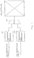
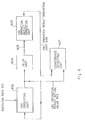
- FIG. 1 shows the general configuration of an ATM switching unit.
- Each cell is transmitted via a large capacity ATM transmission line (optical transmission line) 101 at a transmission speed of 600Mbps (megabits/second), for example.
- Each transmission line 101 is terminated by a transmission line terminal unit 102, multiplexed by a multiplexer (MUX) 103 and then switched by an ATM switch 104.
- MUX multiplexer
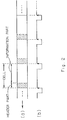
- each cell is multiplexed as shown by (a) of Figure 2 to a predetermined 53-byte time slot and transmitted in the direction indicated by the arrow shown by (a) of Figure 2.
- Each cell comprises a header part containing its destination information, etc., and an information part containing communication information.
- a multiplexed cell is re-multiplexed to a plurality of transmission lines after being inputted from each ATM transmission line 101. Therefore, the cell input timing through the ATM transmission line 101 must be exactly synchronized.
- the synchronizing operation is realized as an operation by a transmission line terminal unit 102 of detecting the head of a cell header applied through each of the ATM transmission lines 101.
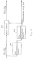
- FIG 3 shows the general configuration of each of the transmission line terminal units 102 for realizing the above described synchronizing operation.
- An HEC (described later) synchronizing circuit 301 detects the input timing of the header part of a cell 304 inputted from the transmission line 101.
- a cell synchronization determining circuit 302 determines the stable input timing of a cell by detecting in the HEC synchronizing circuit 301 the repetition of the input timing of a header part of a plurality of cells 304. Then, the circuit 302 outputs a cell synchronizing pulse 305 as shown in Figure 2.
- a cell 304 temporarily stored by a delay circuit 303 is outputted toward the MUX 103 shown in Figure 1 according to the timing shown in (a) and (b) of Figure 9.
- each of the cells 304 transmitted from each of the transmission line terminal units 102 is multiplexed according to the cell synchronizing pulse 305 provided by each of the transmission line terminal units 102.
- a header part of a cell comprises 5-byte data, the last byte of which is called an HEC (Header Error Checker).
- the HEC is a CRC code added to 4-byte data transmitted as destination information on the sending side. That is, on the sending side, a one-byte CRC code can be obtained as a remainder of a division by dividing a polynomial in the binary representation comprising the above described 4-byte data to be transmitted by the generated polynomial x8 + x2 + x + 1.
- the 5-byte data of a header part of a sending cell can be generated by adding the CRC code to the 4-byte data to be transmitted.
- the HEC synchronizing circuit 301 ( Figure 3) sequentially retrieves 5-serial-byte data by moving each of their positions forward by one byte each. Then, a CRC operation is performed such that a binary polynomial comprising 5-byte-data to be received is divided by the generated polynomial used on the sending side. As indicated by the principle of the above described CRC operation, the remainder of the division in which a 5-byte coded-word polynomial is divided by a generated polynomial used on the sending side must be "0" if the 5-byte data of a header part are correctly extracted on the receiving side.
- the HEC synchronizing circuit 301 must detect as current input timing of an error-free header part of a cell 304 ( Figure 3) the input timing of 5-byte data to be received when a remainder "0" is obtained in the above described CRC operation. That is, the HEC synchronizing circuit 301 detects the input timing of a header part and simultaneously detects errors therein.
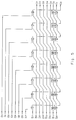
- Figure 4 shows a configuration sample of the prior art technology of the HEC synchronizing circuit for realizing the detecting operation for a header part.
- the HEC synchronizing circuit 301 must sequentially retrieve 5-serial-byte data by moving each of their positions forward by one byte each. Then, a CRC operation is performed such that a binary polynomial comprising 5-byte-data to be received is divided by the generated polynomial used on the sending side.
- the data is sequentially received in a byte unit, stored in a flip-flop (FF) 4020, sequentially shifted in a byte unit in FF4021 - FF4024, and 5-byte receiving data are retrieved as the output of FF4020 - 4024.
- FF flip-flop
- each CRCC 401 a CRC operation is performed such that each byte in the 5-byte data is divided by a generated polynomial x8 + x2 + x + 1.
- an operation result obtained by the operation in the previous CRCC 401 (the remainder after dividing each byte datum by a generated polynomial) is provided to the next CRCC 401.
- the all "0" data are applied as an initial value to the first CRCC 401.
- Figure 5 shows the circuit configurations of each of the CRCCs 4011 - 4015 shown in Figure 4.
- a0 - a7 are received data outputted from the FF 402
- b0 - b7 are results of the CRC operation in the previous CRCC 401
- c0 - c7 are results of the CRC operation in the present CRCC 401.
- a7, b7, and c7 are MSBs, that is, the most significant bits
- a0, b0, and c0 are LSBs, that is, the least significant bits.
- the circuit configuration shown in Figure 5 is well-known for performing a CRC operation and comprises a combination of exclusive logical sum (EOR) elements.
- the conventional HEC synchronizing circuit requires five serially connected CRC operating circuits (CRCC) 4011 - 4015, and the hardware is configured in a large scale. Specifically, in the ATM switching method, the hardware must be configured in the smallest possible scale because 1-byte data are processed at a very high clock speed of 18.75 - 75 MHz.
- CRC CRC operating circuits
- the above described problem is not limited to an HEC synchronizing circuit in an ATM switching method, but also occurs in a CRC operating unit for sequentially performing a CRC operation to detect the segmentation of data containing a CRC code and for detecting errors in the data.
- the present invention has been developed based on the above described background, and an object of the present invention is to realize a CRC operation in small scale hardware.
- the number of serially connected CRC operating circuits must correspond to the data length of a header part.
- a CRC operation for conducting the HEC synchronization can be realized only by one CRC operating unit and one CRC operation result derivation unit. Taking a coset into account according to the CCITT (International Telegraph and Telephone Consultative Committee) recommendations, the hardware can be configured in a smaller scale than in the prior art technology.
- Figure 6 is a block diagram for explaining the principle of the present invention, and shows an HEC synchronizing unit for detecting errors in the header part of a cell in the asynchronous transfer mode (ATM) switching method and for performing a cell synchronizing operation.
- ATM asynchronous transfer mode
- a CRC operating unit 602 performs a cyclic redundancy check (CRC) in which received data 601 are divided by a predetermined generated polynomial with a CRC operation result actual value 603 obtained in the previous operation as an initial value in response to received data 601 applied in a byte unit. Then, it outputs the CRC operation result actual value 603 as a remainder.
- CRC cyclic redundancy check
- a delay unit 604 delays the output of the CRC operation result actual value 603 by the time in which a header part of the received data 601 takes to be inputted.
- a CRC operation result derivation unit 605 outputs a value as a CRC operation result derivation value 606 as if it were obtained as a result of a CRC operation performed for all the receiving data of a header part including a CRC code of the length of the above described header part using as an initial value the CRC operation result actual value 603 outputted by the delay unit 604.
- the unit 605 comprises a plurality of logical circuits for outputting a value as a CRC operation result derivation value 606 as if it were obtained as a result of a CRC operation performed for all the receiving data of a header part including a CRC code of the length of the above described header part using an initial value having one bit value different from the values of the other bits.
- Each logical circuit is provided for each initial value having a different value bit placed at a different position.
- Each of the logical circuits is connected such that the CRC operation result derivation value 606 can be obtained as an exclusive logical sum of output values of the logical circuits each corresponding to an initial value having a different value at a different bit position .
- a coincidence detecting unit 607 compares the CRC operation result actual value 603 outputted by the CRC operating unit 602 with the CRC operation result derivation value 606 outputted by the CRC operation result derivation unit 605. It then detects the input timing of received data containing no errors in the header part provided with a CRC code.
- the above described configuration of the present invention relates to an HEC synchronizing unit in the ATM switching method.
- the present invention is not limited to this application, but can be used to detect the segmentation of data containing a CRC code by sequentially performing a CRC operation for detecting errors in data.
- the operation result of the CRC operation of the header part takes a unique value in response to the initial value.
- the CRC operation result derivation unit 605 (corresponding to the CCR) performs a deriving operation to derive as the CRC operation result derivation value 606 an operation result in response to any initial value.
- the CRC operating unit 602 performs a CRC operation for each piece of sequentially received data in a byte unit, and the CRC operation result actual value 603 obtained by each CRC operation is used as the initial value of the next CRC operation.
- the CRC operation result actual value 603 obtained in the CRC operation performed on the 5th byte (in the HEC portion) of a 5-byte header part is equal to the CRC operation result derivation value 606 derived by the CRC operation result derivation unit 605 using the initial value used when a CRC operation is performed for the byte four bytes before the present one, that is, the first byte of the header part.
- the initial value is equal to the CRC operation result actual value 603 obtained in the CRC operation performed for the 5 bytes before the present byte.
- the delay unit 604 delays the CRC operation result actual value 603 by 5 bytes corresponding to the data length of a header part, for example. Then, the CRC operation result derivation unit 605 derives the CRC operation result derivation value 606 as if it were obtained as a result of a CRC operation performed for the whole 5-byte header using as an initial value the CRC operation result actual value 603 for the data 5 bytes before the present received data 601 (data to be processed) in the present CRC operation.
- CRC operation result derivation value 606 is compared with the CRC operation result actual value 603, the input timing of receiving data containing no errors in a header part can be detected as the timing indicating "coincidence" between these values, thus establishing the HEC synchronization.
- the general configuration of the ATM switching unit related to the preferred embodiment of the present invention is the same as that shown in Figure 1.
- the block configuration of a transmission line terminal unit 102 ( Figure 1) for realizing an HEC synchronizing operation is the same as that shown in Figure 3.
- the feature of the preferred embodiment described below resides in a practical configuration of the HEC synchronizing circuit 301. Before explaining the configuration, the operational principle of the preferred embodiment is described.
- one-byte data comprising all "0s” are applied as an initial value to the first CRCC 401, and an operation result of a CRC operation in each of the CRCCs 401 is provided to the next CRCC 401.
- the input timing of a 5-byte header part is detected with the operation result in the 5th CRCC 4015 obtained as "0".
- an initial value since an initial value must be set as all "0s", five CRCCs for performing a CRC operation in a byte unit must be connected, and the hardware is thus configured in a large scale.
- a result of a CRC operation for a 5-byte header part (a remainder of a division in which the 5-byte data of a header part is divided by a generated polynomial using the above described initial value) is uniquely obtained in response to an initial value when a CRC operation is performed for a 5-byte header part and when an initial value in the operation does not comprise all "0s" but any other initial values.
- Figure 13 shows results of operations in which only one bit in an initial value comprising eight bits, that is, one byte, contains "1" when a CRC operation is performed for a 5-byte header part.
- a result of a CRC operation performed for a 5-byte header part can be derived when an initial value can be any value. That is, in any initial value comprising 8 bits, a bit indicating the value "1" is extracted, and an operation result of an initial value having the above described bit as the only bit containing the value "1" is extracted from Figure 13.
- a result of a CRC operation performed on a 5-byte header part comprising the above described initial value can be derived as a value sequentially indicating exclusive OR for each bit in each operation result. For example, when an 8-bit initial value is "00100101", the 0-th, 2nd, and 5th bits indicate "1".
- a result of a CRC operation for a 5-byte header part can be derived as the value "10001001" obtained by sequentially calculating an exclusive logical sum for each bit of the operation results "01100010", “10001111”, and "01100100” obtained in (a), (c), and (f) in Figure 13.
- the present preferred embodiment is based on the above described fact. That is, a CRC operation is performed on each piece of sequentially received 1-byte data, and a result obtained in each CRC operation is used as the initial value of the next CRC operation.
- the result obtained in the CRC operation performed for the 5th byte of a 5-byte header part is equal to the operation result derived according to Figure 13 for the initial value used when a CRC operation is performed on the byte four bytes before the present one, that is, the first byte of the header part.
- the initial value is equal to the result of the CRC operation for the byte 5 bytes before the present one.
- a circuit is provided to derive a value as if it were obtained as a result of a CRC operation performed for a 5-byte header part using as an initial value the result of the CRC operation for the data which is 5 bytes before those to be processed in the present CRC operation.
- the input timing of the 5th byte of the header part that is, the HEC portion, is detected as the timing at which the derivation result and the result of the CRC operation for the data being processed are equivalent. The synchronization of a header part can thus be established.
- Figure 7 shows the principle for explaining the present preferred embodiment for realizing the above described operations.
- Receiving data 705 sequentially applied in a byte unit from an ATM transmission line 101 ( Figure 1) are temporarily stored in the FF7040 and then applied to a CRC operating circuit (CRCC) 701.
- CRCC CRC operating circuit
- the CRCC 701 performs for the receiving data 705 applied in a byte unit from the FF7040 a CRC operation in which the above described receiving data 705 are divided by the generated polynomial x8 + x2 + x + 1 using as an initial value a CRC operation result actual value 706 obtained in the previous CRC operation, and then it outputs as a remainder an 8-bit CRC operation result actual value 706.
- the CRC operation result actual value 706 is delayed by 5 input timings by the five serially connected FF 7041 - 7045, and applied to a CRC code correcting circuit (CCR) 702.
- CCR CRC code correcting circuit
- the CCR 702 outputs a value as an 8-bit CRC operation result derivation value 707 as if it were obtained as a result of a CRC operation performed for a 5-byte header part using as an initial value the CRC operation result actual value 706 outputted by the CRCC 701 5 input timings before the present process timing, that is, the initial value used in the CRCC 701 which is 4 input timings before the present process timing.
- a coincidence detecting circuit 703 compares the 8-bit CRC operation result actual value 706 outputted by the CRCC 701 with an 8-bit CRC operation result derivation value 707 outputted by the CCR 702. If all corresponding bits of these values coincide, a determination output 708 indicating coincidence is outputted.
- the FF 7040 - 7045 operate according to a clock CLK synchronized with the input timing of the received data 705.
- the transmission speed of the ATM transmission line 101 shown in Figure 1 is 600 Mbps
- Figure 8 shows the first typical configuration sample of a circuit.
- the CCR 702 comprises a plurality of exclusive logical sum elements (EOR).
- Bit signals c0 - c7 (MSB on the side of c7) corresponds to each bit of the CRC operation result actual value 706 inputted to the FF 7045 shown in Figure 7 and outputted from the CRCC 701 5 input timings before the present process timing, that is, each bit of the initial value in the CRCC 701 4 input timings before the present process timing.
- Bit signals D0 - D7 correspond to each bit of the CRC operation result actual value 706 shown in Figure 7.
- Each of 8010 - 8017 enclosed in dotted lines performs a conversion process indicated by (a) - (h) shown in Figure 13.
- the 8010 is a circuit unit for outputting "01100010" when the 0-th bit c0 of an initial value indicates "1" and the 1st bit c1 to the 7th bit c7 indicate "0".
- An exclusive logical sum is sequentially obtained in a bit unit for each operation result shown in Figure 13 by connecting each of the portions 8010 - 8017 enclosed in dotted lines through an exclusive logical sum element as shown in Figure 8.
- an exclusive logical sum element is applied to the bit position where "1" is outputted by a corresponding portion 801 enclosed in dotted lines according to Figure 13.
- a byte data applied to the portion 8017 comprise all "0s" as shown in Figure 8.
- Figure 9 shows an operational timing chart for explaining the principle configuration of the present preferred embodiment shown in Figures 5, 7, and 8.
- the receiving data 705 are entered in a byte unit as shown by (a) of Figure 9 after synchronized with the clock CLK, having a frequency of 75MHz, for example, as shown by (b) of Figure 9.
- the data are stored by the FF 7040 at the rise timing of the clock CLK, and the output is applied to the CRCC 701 at the timing shown by (c) of Figure 9.
- the CRC operation result actual value 706 is outputted from the CRCC 701 to the coincidence detecting circuit 703.
- the content of the CRC operation result derivation value 707 is outputted from the CCR 702, and it is a derivation value corresponding to the CRC operation result actual value 706 outputted from the CRCC 701 5 input timings before the present process timing as shown by (d) of Figure 9.
- the following values can be obtained at the timing at which the 5th byte of a header part, that is, the portion B HEC of the HEC, is applied to the CRCC 701.
- a53 shown by (d) of Figure 9 can be obtained from the FF 7045 as the CRC operation result actual value 706 at 5 inputs timing before the present process timing corresponding to A53, that is, the 53rd byte (last byte) of the previous cell of the present cell.
- the CRC operation result derivation value 707 corresponding to a53 can be obtained from the CCR 702. If there are no errors in the data of the header part, a determination output 708 indicating coincidence is outputted by the coincidence detecting circuit 703.
- Figure 10 shows the second example of a circuit configuration.
- the portions 8010 - 8017 enclosed in broken lines can be connected in any order according to the characteristics of an exclusive logical sum.
- each exclusive logical sum element is omitted.
- five exclusive logical sum elements can be omitted if an initial value c7 is directly applied to the next portion 801 enclosed in broken lines.
- a CCR 702 can be configured with the smallest possible number of elements, and the circuit scale can thus be further reduced.
- Figure 11 shows a practical configuration for explaining the preferred embodiment of the HEC synchronizing circuit 301 shown in Figure 3 of the present invention.
- the basic configuration and operation are the same as those of Figure 7.
- the CCR 1102 corresponds to the CCR 702 shown in Figure 7
- the coincidence detecting circuit 1103 corresponds to the circuit 703 shown in Figure 7
- the FFs 11040 - 11045 correspond to the FFs 7040 - 7045
- the receiving data 1105 correspond to the data 705 shown in Figure 7
- the CRC operation result actual value 1106 corresponds to the value 706 shown in Figure 7
- the CRC operation result derivation value 1107 corresponds to the value 707 shown in Figure 7
- the determination output 1108 corresponds to the output 708 shown in Figure 7.
- Figure 11 differs from that of Figure 7 in that it comprises only two CRCCs 11011 and 11012, two additional FFs 11047 and 11048 for retaining each output, an AND element 610, and an exclusive logical element 611.
- the configuration of the preferred embodiment shown in Figure 11 follows the circuit configuration according to the CCITT recommendations.
- an exclusive logical sum is calculated with each bit of a CRC code obtained as a CRC operation result and each bit of a code called "coset” indicating "01010101", and the operation result is stored as an HEC in the header part of a cell according to the recommendations when on a sending side of a cell a CRC operation is performed for 4-byte header data and a 1-byte HEC is added to the data. Therefore, on the receiving side, an exclusive logical sum is calculated again for the HEC portion with the receiving data 1105 outputted by the FF 11040 and the above described coset "01010101" to decode the original CRC code, and then perform a CRC operation.
- the exclusive logical sum element 611 and CRCC 11012 shown in Figure 11 are provided to perform the necessary processes involved.
- the exclusive logical sum element 611 is used as an element to obtain an exclusive logical sum for each bit using 1-byte (8-bit) receiving data 1105 provided by the FF 11040 and 8-bit coset "01010101".
- Figure 12 is an operational timing chart for explaining the practical configuration of the preferred embodiment shown in Figure 11.
- the 5th byte of a header part that is, the HEC portion B HEC
- the exclusive logical sum element 611 subtracts a coset from the HEC data, and they are inputted to the CRCC 11012.
- a b HEC shown by (f) of Figure 12 is outputted as a CRC operation result true value 1109 by the FF 11048
- an a53 shown by (h) of Figure 12 corresponding to A53, the 53rd byte (last byte) and the previous cell of the present input cell is obtained as a CRC operation result actual value 1106.
- a CRC operation result derivation value 1107 corresponding to the above described a53 can be obtained by the CCR 1102. If no errors have arisen in the data of the header part, a determination output 1108 indicating a coincidence is outputted by the coincidence detecting circuit 1103.
- the configuration shown in Figure 11 differs from that shown in Figure 7 in a clock for operating each FF 1104.
- a transmission method called SONET is used in the ATM transmission line 101 shown in Figure 1. Therefore, in the preferred embodiment shown in Figure 11, a signal component of a pulse OH indicating overhead of the SONET is subtracted from an AND element 610.
- the resultant clock FF CLK operates each FF 1104.
- no FF 1104 continues its operation if the receiving data 1105 equals the overhead of the SONET.
- an HEC synchronizing circuit 301 ( Figure 3) can be realized in conformity with the CCITT recommendations related to the ATM switching method.
Applications Claiming Priority (3)
| Application Number | Priority Date | Filing Date | Title |
|---|---|---|---|
| JP48406/91 | 1991-03-13 | ||
| JP4840691 | 1991-03-13 | ||
| JP4840691A JP2655547B2 (ja) | 1991-03-13 | 1991-03-13 | Crc演算方法及びatm交換方式におけるhec同期装置 |
Publications (3)
| Publication Number | Publication Date |
|---|---|
| EP0503667A2 true EP0503667A2 (fr) | 1992-09-16 |
| EP0503667A3 EP0503667A3 (en) | 1993-05-19 |
| EP0503667B1 EP0503667B1 (fr) | 2002-01-30 |
Family
ID=12802426
Family Applications (1)
| Application Number | Title | Priority Date | Filing Date |
|---|---|---|---|
| EP19920104404 Expired - Lifetime EP0503667B1 (fr) | 1991-03-13 | 1992-03-13 | Méthode d'opération pour CRC et unité de synchronisme HEC (Détection d'erreur en tête) pour la méthode de commutation ATM |
Country Status (5)
| Country | Link |
|---|---|
| US (1) | US5345451A (fr) |
| EP (1) | EP0503667B1 (fr) |
| JP (1) | JP2655547B2 (fr) |
| CA (1) | CA2062855C (fr) |
| DE (1) | DE69232384T2 (fr) |
Cited By (7)
| Publication number | Priority date | Publication date | Assignee | Title |
|---|---|---|---|---|
| EP0632613A1 (fr) * | 1993-06-29 | 1995-01-04 | Motorola, Inc. | Méthode et appareil de restitution de données dans un système de radio communication |
| EP0682790A1 (fr) * | 1993-11-22 | 1995-11-22 | Motorola, Inc. | Procede et systeme de synchronisation de codeurs et decodeurs des reseaux de telecommunications en cas de detection d'erreurs |
| EP0838969A2 (fr) * | 1996-10-24 | 1998-04-29 | AT&T Corp. | Mise en trame rapide du protocol ATM, utilisé seul, par le contrÔle des erreurs dans l'en-tête |
| GB2323503A (en) * | 1997-03-05 | 1998-09-23 | Nec Corp | ATM cell synchronisation circuit |
| WO1999026448A1 (fr) * | 1997-11-13 | 1999-05-27 | Virata Limited | Synchronisation de trains de bits |
| EP1496637A1 (fr) * | 2001-10-29 | 2005-01-12 | Samsung Electronics Co., Ltd. | Dispositif et procédé pour la transmission/réception d'informations de détection d'erreur dans un système de communications |
| CN102195750A (zh) * | 2010-03-03 | 2011-09-21 | 株式会社日立制作所 | 数据传送装置及数据传送系统 |
Families Citing this family (30)
| Publication number | Priority date | Publication date | Assignee | Title |
|---|---|---|---|---|
| ES2068105B1 (es) * | 1992-11-30 | 1995-11-01 | Alcatel Standard Electrica | Metodo y dispositivo de deteccion y correccion de errores en cabeceras de celulas atm. |
| SE501884C2 (sv) * | 1993-10-12 | 1995-06-12 | Ellemtel Utvecklings Ab | Synkroniserande kretsarrangemang fastställer gräns mellan konsekutiva paket |
| KR970004256B1 (ko) * | 1994-06-29 | 1997-03-26 | 한국전기통신공사 | 순환코드를 이용한 프레임/버스트 동기 및 에러 검출장치 |
| US5771249A (en) * | 1994-09-02 | 1998-06-23 | Toyo Communication Equipment Co., Ltd. | ATM cell synchronous system |
| US5530806A (en) * | 1994-12-15 | 1996-06-25 | At&T Corp. | Method and apparatus for storing and retrieving routing information in a network node |
| KR970009756B1 (ko) * | 1994-12-23 | 1997-06-18 | 한국전자통신연구원 | 에러 정정 및 프레임 복구용 순환 선로 부호화 장치 |
| JP3454962B2 (ja) * | 1995-03-23 | 2003-10-06 | 株式会社東芝 | 誤り訂正符号の符号器及び復号器 |
| JP3234130B2 (ja) * | 1995-05-30 | 2001-12-04 | 三菱電機株式会社 | 誤り訂正符号復号化方法およびこの方法を用いる回路 |
| FR2759227B1 (fr) * | 1997-02-04 | 1999-04-16 | Fihem | Procede pour associer des donnees a des cellules atm |
| JP3575215B2 (ja) * | 1997-03-05 | 2004-10-13 | 株式会社日立製作所 | パケット通信方法及び通信端末装置 |
| US6038694A (en) * | 1997-03-24 | 2000-03-14 | Cisco Systems, Inc. | Encoder for producing a checksum associated with changes to a frame in asynchronous transfer mode systems |
| US6061741A (en) * | 1997-05-28 | 2000-05-09 | International Business Machines Corporation | Method and apparatus for synchronization of connectionless applications across a network by using simple encryption tokens |
| US5923681A (en) * | 1998-02-24 | 1999-07-13 | Tektronix, Inc. | Parallel synchronous header correction machine for ATM |
| US6678842B1 (en) | 1998-12-14 | 2004-01-13 | Agere Systems Inc. | Communications system and associated deskewing methods |
| US6909727B1 (en) | 1998-12-14 | 2005-06-21 | Agere Systems Inc. | Communications system and associated methods with out-of-band control |
| US6775302B1 (en) | 1998-12-14 | 2004-08-10 | Agere Systems Inc. | Communications system with symmetrical interfaces and associated methods |
| US6675327B1 (en) | 1998-12-14 | 2004-01-06 | Agere Systems Inc. | Communications system including lower rate parallel electronics with skew compensation and associated methods |
| US6480977B1 (en) | 1999-10-29 | 2002-11-12 | Worldcom, Inc. | Multi-protocol monitor |
| US6535925B1 (en) * | 1999-11-09 | 2003-03-18 | Telefonaktiebolaget L M Ericsson (Publ) | Packet header compression using division remainders |
| US20020155936A1 (en) * | 2001-04-23 | 2002-10-24 | Wied Randy C. | Modular pouch machine |
| US6804220B2 (en) * | 2001-05-07 | 2004-10-12 | Qualcomm Incorporated | Method and apparatus for generating control information for packet data |
| US6928608B2 (en) * | 2001-08-14 | 2005-08-09 | Optix Networks Ltd. | Apparatus and method for accelerating cyclic redundancy check calculations |
| JP2003078421A (ja) * | 2001-09-04 | 2003-03-14 | Canon Inc | 符号系列の先頭位置検出方法とその装置、それを用いた復号方法とその装置 |
| US6968492B1 (en) * | 2002-03-28 | 2005-11-22 | Annadurai Andy P | Hardware-efficient CRC generator for high speed communication networks |
| US20040158794A1 (en) * | 2002-07-19 | 2004-08-12 | Niesen Joseph W. | Reduced overhead CRC functionality for packets and link layer superframes |
| US7320101B1 (en) * | 2003-08-19 | 2008-01-15 | Altera Corporation | Fast parallel calculation of cyclic redundancy checks |
| US7613991B1 (en) | 2003-08-19 | 2009-11-03 | Altera Corporation | Method and apparatus for concurrent calculation of cyclic redundancy checks |
| CN1798014B (zh) * | 2004-12-20 | 2010-04-28 | 华为技术有限公司 | 一种循环冗余编码定帧方法 |
| US8082480B2 (en) | 2007-06-27 | 2011-12-20 | Presagis | Distributed checksum computation |
| EP2096884A1 (fr) | 2008-02-29 | 2009-09-02 | Koninklijke KPN N.V. | Réseau de télécommunication et procédé d'accès de réseau en fonction du temps |
Citations (2)
| Publication number | Priority date | Publication date | Assignee | Title |
|---|---|---|---|---|
| EP0003480A2 (fr) * | 1977-12-30 | 1979-08-22 | Siemens Aktiengesellschaft | Dispositif pour convertir des informations binaires à l'aide de bits de contrôle |
| EP0396403A1 (fr) * | 1989-05-04 | 1990-11-07 | Nortel Networks Corporation | Synchronisation de trame d'un train de données |
Family Cites Families (4)
| Publication number | Priority date | Publication date | Assignee | Title |
|---|---|---|---|---|
| US4397020A (en) * | 1980-09-11 | 1983-08-02 | Bell Telephone Laboratories, Incorporated | Error monitoring in digital transmission systems |
| US4700350A (en) * | 1986-10-07 | 1987-10-13 | Douglas Phillip N | Multiple phase CRC generator |
| JP2816223B2 (ja) * | 1990-03-02 | 1998-10-27 | 株式会社日立製作所 | セル同期回路 |
| CA2059396C (fr) * | 1991-01-16 | 1996-10-22 | Hiroshi Yamashita | Dispositif compact servant a verifier les erreurs d'en-tete dans des cellules en mode de transfert asynchrone |
-
1991
- 1991-03-13 JP JP4840691A patent/JP2655547B2/ja not_active Expired - Fee Related
-
1992
- 1992-03-10 US US07/848,170 patent/US5345451A/en not_active Expired - Lifetime
- 1992-03-12 CA CA 2062855 patent/CA2062855C/fr not_active Expired - Fee Related
- 1992-03-13 EP EP19920104404 patent/EP0503667B1/fr not_active Expired - Lifetime
- 1992-03-13 DE DE1992632384 patent/DE69232384T2/de not_active Expired - Fee Related
Patent Citations (2)
| Publication number | Priority date | Publication date | Assignee | Title |
|---|---|---|---|---|
| EP0003480A2 (fr) * | 1977-12-30 | 1979-08-22 | Siemens Aktiengesellschaft | Dispositif pour convertir des informations binaires à l'aide de bits de contrôle |
| EP0396403A1 (fr) * | 1989-05-04 | 1990-11-07 | Nortel Networks Corporation | Synchronisation de trame d'un train de données |
Non-Patent Citations (1)
| Title |
|---|
| ELECTRONICS AND COMMUNICATIONS IN JAPAN vol. 73, no. 5, 1 May 1990, NEW YORK US pages 99 - 108 TOKUHIRO KITAMI 'Synchronization method employing a cyclic redundancy check in an asynchronous transport system' * |
Cited By (11)
| Publication number | Priority date | Publication date | Assignee | Title |
|---|---|---|---|---|
| EP0632613A1 (fr) * | 1993-06-29 | 1995-01-04 | Motorola, Inc. | Méthode et appareil de restitution de données dans un système de radio communication |
| EP0682790A1 (fr) * | 1993-11-22 | 1995-11-22 | Motorola, Inc. | Procede et systeme de synchronisation de codeurs et decodeurs des reseaux de telecommunications en cas de detection d'erreurs |
| EP0682790A4 (fr) * | 1993-11-22 | 1998-05-20 | Motorola Inc | Procede et systeme de synchronisation de codeurs et decodeurs des reseaux de telecommunications en cas de detection d'erreurs. |
| EP0838969A2 (fr) * | 1996-10-24 | 1998-04-29 | AT&T Corp. | Mise en trame rapide du protocol ATM, utilisé seul, par le contrÔle des erreurs dans l'en-tête |
| EP0838969A3 (fr) * | 1996-10-24 | 1999-03-24 | AT&T Corp. | Mise en trame rapide du protocol ATM, utilisé seul, par le contrÔle des erreurs dans l'en-tête |
| GB2323503A (en) * | 1997-03-05 | 1998-09-23 | Nec Corp | ATM cell synchronisation circuit |
| GB2323503B (en) * | 1997-03-05 | 1999-02-10 | Nec Corp | ATM cell synchronization circuit |
| WO1999026448A1 (fr) * | 1997-11-13 | 1999-05-27 | Virata Limited | Synchronisation de trains de bits |
| EP1496637A1 (fr) * | 2001-10-29 | 2005-01-12 | Samsung Electronics Co., Ltd. | Dispositif et procédé pour la transmission/réception d'informations de détection d'erreur dans un système de communications |
| CN102195750A (zh) * | 2010-03-03 | 2011-09-21 | 株式会社日立制作所 | 数据传送装置及数据传送系统 |
| CN102195750B (zh) * | 2010-03-03 | 2015-04-01 | 株式会社日立制作所 | 数据传送装置及数据传送系统 |
Also Published As
| Publication number | Publication date |
|---|---|
| US5345451A (en) | 1994-09-06 |
| EP0503667A3 (en) | 1993-05-19 |
| JPH04284753A (ja) | 1992-10-09 |
| DE69232384D1 (de) | 2002-03-14 |
| EP0503667B1 (fr) | 2002-01-30 |
| DE69232384T2 (de) | 2002-09-12 |
| CA2062855C (fr) | 1997-04-01 |
| JP2655547B2 (ja) | 1997-09-24 |
| CA2062855A1 (fr) | 1992-09-14 |
Similar Documents
| Publication | Publication Date | Title |
|---|---|---|
| US5345451A (en) | Cyclic redundancy check operating method and a head error checker synchronizing unit in an asynchronous transfer mode switching process | |
| EP0448074B1 (fr) | Dispositif de synchronisation de cellules transmises en mode de transfert asynchrone | |
| US5384774A (en) | Asynchronous transfer mode (ATM) payload synchronizer | |
| US7710980B2 (en) | Synchronization system and method | |
| EP0600380B1 (fr) | Procédé et dispositif de détection et correction des erreurs dans les segments de tête des cellules ATM | |
| EP0735728B1 (fr) | Procédé de codage 5B4T | |
| US7370263B1 (en) | Hardware efficient CRC generator for high speed communication networks | |
| US5402429A (en) | Error detection and correction device to detect and correct single bit errors in a transmitted sequence of bits | |
| US4796282A (en) | Frame synchronization detection system | |
| US6873621B2 (en) | System for controlling AAL1 cell bandwidth | |
| EP1142242B1 (fr) | Systeme de communication et procedes de redressement correspondants | |
| JPH07177159A (ja) | 一連の異なるエンティティの形で供給される所与のアプリケーション用の情報のatmセルによる伝送方法及びこの方法を実施するための装置 | |
| US7126950B2 (en) | Method and system for transmission and reception of asynchronously multiplexed signals | |
| US5694405A (en) | Encoder and decoder of an error correcting code | |
| US6487176B1 (en) | Measuring method and measuring device for data communication networks | |
| US5280484A (en) | Time-division multiplex communication system with a synchronizing circuit at the receiving end which responds to the coding of words inserted in the transmitted information | |
| US20030118184A1 (en) | Parallel distributed sample descrambling apparatus of passive optical network and method thereof | |
| JP2967748B2 (ja) | Atmセル同期回路 | |
| EP0737390B1 (fr) | Dispositif permettant d'etablir des frontieres de cellules dans un train de bits et de calculer le code de redondance cyclique (crc) | |
| JP2952051B2 (ja) | Atmにおけるセル同期演算回路 | |
| US6449277B1 (en) | Interleaver for parallel 8 bit cell of ATM systems and a method therefor | |
| JP3045879B2 (ja) | 伝送速度不一致検出装置 | |
| KR100267277B1 (ko) | 통신시스템의 셀 경계 식별 장치 | |
| KR970005732B1 (ko) | 비동기전달모드 시스템에서의 순환잉여검사 코드 계산 및 검출장치 | |
| KR19980020862A (ko) | 비동기 전송모드(atm) 셀 기반 전송방식의 프레임 동기장치 |
Legal Events
| Date | Code | Title | Description |
|---|---|---|---|
| PUAI | Public reference made under article 153(3) epc to a published international application that has entered the european phase |
Free format text: ORIGINAL CODE: 0009012 |
|
| AK | Designated contracting states |
Kind code of ref document: A2 Designated state(s): DE FR GB |
|
| PUAL | Search report despatched |
Free format text: ORIGINAL CODE: 0009013 |
|
| AK | Designated contracting states |
Kind code of ref document: A3 Designated state(s): DE FR GB |
|
| 17P | Request for examination filed |
Effective date: 19930608 |
|
| 17Q | First examination report despatched |
Effective date: 19990715 |
|
| GRAG | Despatch of communication of intention to grant |
Free format text: ORIGINAL CODE: EPIDOS AGRA |
|
| GRAG | Despatch of communication of intention to grant |
Free format text: ORIGINAL CODE: EPIDOS AGRA |
|
| GRAH | Despatch of communication of intention to grant a patent |
Free format text: ORIGINAL CODE: EPIDOS IGRA |
|
| RBV | Designated contracting states (corrected) |
Designated state(s): DE FR |
|
| GRAH | Despatch of communication of intention to grant a patent |
Free format text: ORIGINAL CODE: EPIDOS IGRA |
|
| GRAA | (expected) grant |
Free format text: ORIGINAL CODE: 0009210 |
|
| AK | Designated contracting states |
Kind code of ref document: B1 Designated state(s): DE FR |
|
| REF | Corresponds to: |
Ref document number: 69232384 Country of ref document: DE Date of ref document: 20020314 |
|
| ET | Fr: translation filed | ||
| PLBE | No opposition filed within time limit |
Free format text: ORIGINAL CODE: 0009261 |
|
| STAA | Information on the status of an ep patent application or granted ep patent |
Free format text: STATUS: NO OPPOSITION FILED WITHIN TIME LIMIT |
|
| 26N | No opposition filed | ||
| PGFP | Annual fee paid to national office [announced via postgrant information from national office to epo] |
Ref country code: DE Payment date: 20080306 Year of fee payment: 17 Ref country code: FR Payment date: 20080311 Year of fee payment: 17 |
|
| REG | Reference to a national code |
Ref country code: FR Ref legal event code: ST Effective date: 20091130 |
|
| PG25 | Lapsed in a contracting state [announced via postgrant information from national office to epo] |
Ref country code: DE Free format text: LAPSE BECAUSE OF NON-PAYMENT OF DUE FEES Effective date: 20091001 |
|
| PG25 | Lapsed in a contracting state [announced via postgrant information from national office to epo] |
Ref country code: FR Free format text: LAPSE BECAUSE OF NON-PAYMENT OF DUE FEES Effective date: 20091123 |