EP0503595A2 - Belichtungsvorrichtung - Google Patents
Belichtungsvorrichtung Download PDFInfo
- Publication number
- EP0503595A2 EP0503595A2 EP92104183A EP92104183A EP0503595A2 EP 0503595 A2 EP0503595 A2 EP 0503595A2 EP 92104183 A EP92104183 A EP 92104183A EP 92104183 A EP92104183 A EP 92104183A EP 0503595 A2 EP0503595 A2 EP 0503595A2
- Authority
- EP
- European Patent Office
- Prior art keywords
- exposure apparatus
- refractive body
- laser light
- flat plane
- light
- Prior art date
- Legal status (The legal status is an assumption and is not a legal conclusion. Google has not performed a legal analysis and makes no representation as to the accuracy of the status listed.)
- Withdrawn
Links
Images


Classifications
-
- G—PHYSICS
- G03—PHOTOGRAPHY; CINEMATOGRAPHY; ANALOGOUS TECHNIQUES USING WAVES OTHER THAN OPTICAL WAVES; ELECTROGRAPHY; HOLOGRAPHY
- G03F—PHOTOMECHANICAL PRODUCTION OF TEXTURED OR PATTERNED SURFACES, e.g. FOR PRINTING, FOR PROCESSING OF SEMICONDUCTOR DEVICES; MATERIALS THEREFOR; ORIGINALS THEREFOR; APPARATUS SPECIALLY ADAPTED THEREFOR
- G03F7/00—Photomechanical, e.g. photolithographic, production of textured or patterned surfaces, e.g. printing surfaces; Materials therefor, e.g. comprising photoresists; Apparatus specially adapted therefor
- G03F7/20—Exposure; Apparatus therefor
-
- G—PHYSICS
- G03—PHOTOGRAPHY; CINEMATOGRAPHY; ANALOGOUS TECHNIQUES USING WAVES OTHER THAN OPTICAL WAVES; ELECTROGRAPHY; HOLOGRAPHY
- G03F—PHOTOMECHANICAL PRODUCTION OF TEXTURED OR PATTERNED SURFACES, e.g. FOR PRINTING, FOR PROCESSING OF SEMICONDUCTOR DEVICES; MATERIALS THEREFOR; ORIGINALS THEREFOR; APPARATUS SPECIALLY ADAPTED THEREFOR
- G03F7/00—Photomechanical, e.g. photolithographic, production of textured or patterned surfaces, e.g. printing surfaces; Materials therefor, e.g. comprising photoresists; Apparatus specially adapted therefor
- G03F7/70—Microphotolithographic exposure; Apparatus therefor
- G03F7/70408—Interferometric lithography; Holographic lithography; Self-imaging lithography, e.g. utilizing the Talbot effect
-
- G—PHYSICS
- G02—OPTICS
- G02B—OPTICAL ELEMENTS, SYSTEMS OR APPARATUS
- G02B5/00—Optical elements other than lenses
- G02B5/001—Axicons, waxicons, reflaxicons
-
- G—PHYSICS
- G02—OPTICS
- G02B—OPTICAL ELEMENTS, SYSTEMS OR APPARATUS
- G02B5/00—Optical elements other than lenses
- G02B5/18—Diffraction gratings
- G02B5/1876—Diffractive Fresnel lenses; Zone plates; Kinoforms
-
- G—PHYSICS
- G03—PHOTOGRAPHY; CINEMATOGRAPHY; ANALOGOUS TECHNIQUES USING WAVES OTHER THAN OPTICAL WAVES; ELECTROGRAPHY; HOLOGRAPHY
- G03H—HOLOGRAPHIC PROCESSES OR APPARATUS
- G03H1/00—Holographic processes or apparatus using light, infrared or ultraviolet waves for obtaining holograms or for obtaining an image from them; Details peculiar thereto
- G03H1/04—Processes or apparatus for producing holograms
- G03H1/0402—Recording geometries or arrangements
- G03H2001/0439—Recording geometries or arrangements for recording Holographic Optical Element [HOE]
Definitions
- the present invention relates to an apparatus capable of exposing concentric circular periodic grating patterns.
- FIG.1 shows a constitutional drawing of an exposure apparatus in this conventional example.
- numeral 1 is a laser apparatus of such as Ar or He-Cd laser
- numeral 2 is a shutter
- numerals 50 and 51 are reflecting mirrors
- numeral 3 is a variable attenuator
- numeral 5 is a beam expander lens
- numeral 6 is a spatial filter
- numeral 7 is a collimator lens
- numerals 52 and 53 are convex lenses
- numeral 10 is a sample substrate
- numeral 11 is a photosensitive film formed over the sample substrate.
- the laser light passes through this aperture, to be converted into a plane-wave beam whose diameter is expanded by the collimator lens 7 (insertion of the spatial filter 6 is for removing noises caused by defects or stains on lenses and mirrors).
- This plane-wave beam is converted into a converging light 54a by a convex lens 52 having a long focal length, while a part of this converging light is converted into a diverging light 54b by a convex lens having a short focal length. Then, these two light fluxes are projected onto a sample substrate 10.
- FIG.2(a) is an explanatory drawing showing the principle of forming a periodic pattern by an exposure apparatus of prior art
- FIG.2(b) is an explanatory sectional view of a grating after the development.
- an interference pattern produced by the light fluxes 54a and 54b of a wavelength ⁇ which impinge the substrate surface with respective incident angles of ⁇ A and ⁇ B , has a period ⁇ in the direction including the incident plane (in the direction of radius vector) and it is expressed by the following Equation 1.
- ⁇ / ⁇ 1/(sin ⁇ A + sin ⁇ B ).
- Equation 1 On the photosensitive film after the development, is obtained a grating 55 of a concentric circular shape as shown in FIG.2(b).
- a grating pattern obtained by an exposure apparatus of prior part is limited to a chirped grating (such as grating lens, Fresnel lens) in accordance with a modulation characteristic wherein the pitch at the center of the pattern is zero; and it is not capable of exposing a concentric circular periodic grating pattern having other modulation characteristic than the above-mentioned characteristic (such as concentric grating coupler, concentric focusing grating coupler).
- a chirped grating such as grating lens, Fresnel lens
- the present invention purposes to offer an exposure apparatus, which is simple, of low cost, and giving an excellent accuracy in its pattern periodicity and uniformity, and further is capable of exposing concentric circular periodic patterns with modulated pitch in the radial direction.
- the exposure apparatus of the present invention comprises: a laser light source, a refractive body for letting the laser light transmit therethrough and refract, and a photosensitive film formed on a flat plane which is substantially perpendicular to the optical axis of the laser light, wherein the improvement is that the refracting surface of said refractive body is a surface of revolution having the optical axis as its axis of revolution, light fluxes refracting at respective paired diagonal generatrices of the refracting surface intersect to each other in the vicinity of the optical axis, and interfere to each other to form a fringe having concentric circular periodic bright and dark parts, whereto the photosensitive film is exposed.
- concentric circular periodic grating patterns having pitch modulated in the radius vector direction can be exposed with a good contrast, and a fine control of the period modulation is also achievable by the position adjustment of the exposure plane.
- the exposure region can be specified, and a combination of grating patterns with different exposure conditions on the same exposure plane becomes possible.
- the apparatus can be constituted with a simple combination of a laser light source and low-cost optical elements.
- the accuracy of the periodic pattern is determined by the accuracy of optical lenses which generally have the long actually working history as the high-accuracy fabricated elements, an excellent periodicity accuracy is achievable.
- the exposure area is determined by the size of the lens, exposures of large area become possible.
- FIG.3 shows a cross-sectional view of a constitutional drawing of an exposure apparatus of one embodiment of the present invention.
- light emitted from a laser light source 1 is led through a shutter 2, a variable attenuator 3, a quarter-wave plate 4, a beam expander lens 5, a spatial filter 6, a collimator lens 7, a ND filter 8a, a patterning mask 8b, an interference lens 9, to a photosensitive film which is formed on a sample substrate 10.
- the ND filter 8a has different transmissions with boundaries of circle or a group of circles whose center is set at the optical axis of the system
- the patterning mask 8b is a light-masking film, which has a pattern of axial symmetry formed on a transparent substrate.
- the symmetric axis (center axis) of the light-masking film 8b is adjusted in a manner to coincide with the center axis 9L of the interference lens 9, by means of a known X-Y axis translation stage.
- the interference lens 9 has a form of rotation symmetry with respect to its axis 9L, an incident surface 9P of a flat plane, and an exit surface 9S formed in a surface of revolution close to the circular conical surface.
- the interference lens 9 is constituted on or fixed to the X-Y axis translation stage and also on an X-Y axis tilting stage, and thereby, the center axis 9L is adjusted in a manner to coincide with the optical axis of the laser beam 101.
- the sample substrate 10 is constituted on or fixed to an X-Y-Z axis translation stage and also on or to an X-Y axis tilting stage, and thereby it is adjustable in a manner that the surface of the sample substrate 10 intersects perpendicularly with respect to the center axis 9L, as well as, is adjustable along the axis 9L, namely in the direction along an arrow mark 13.
- transmission of the light issued from the laser light source 1 is controlled by a shutter 2, and its light intensity is adjusted stepwisely by a variable attenuator.
- This light beam is converted into a circularly polarized light by letting it pass through the quarter-wave plate 4, being converted into a converging beam by the beam expander lens 5 and then being focused inside a circular aperture of the spatial filter 6.
- the filter 6 passes through the filter 6, the light is converted into a plane wave whose beam diameter is expanded by the collimator lens 7.
- This plane wave passes through the ND filter 8a and then the patterning mask 8b. Thereby, a fraction of the plane wave is attenuated and masked, and then hits the incident surface 9P of the interference lens 9 at right angle.
- the plane wave is refracted at the exit surface 9S as shown by light rays 12a, 12b, 12A, and 12B, finally to be projected onto the photosensitive film 11.
- the insertion of the quarter-wave plate 4 is in order to keep the rotation symmetry of the light as a vector wave by making it into a circularly polarized light. This is in order to keep the rotation symmetry of the interference fringe.
- light rays 12a and 12A and light rays 12b and 12B are respectively placed at mutually diagonal positions with respect to the center axis 9L on the same circle.
- the light ray 12a interferes with the light ray 12B which is on a circle slightly inside a circle whereon the light ray 12a is
- the light ray 12A interferes with the light ray 12b which is on a circle slightly inside a circle on which the light ray 12A is.
- a concentric circular interference fringe having its center on the center axis 9L is formed.
- a concentric circular periodic grating pattern can be formed.
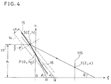
- FIG.4 shows a relation between a sectional shape of the exit surface of the interference lens and the refracted light rays in the exposure apparatus of the embodiment of the present invention.
- the exit surface 9S of the interference lens is formed as a surface of revolution having a curve 16 as its generatrix curve and a ⁇ axis (center axis 9L) as its axis of revolution.
- the curve 16 has two asymptotes which are parallel straight lines 14 and 15 both forming the intersecting angle ⁇ with respect to the ⁇ axis, and has an inflection point P.
- Equation 2 h/h0 is obtained from Equation 2
- ⁇ is obtained from Equation 3
- ⁇ is obtained from Equation 4
- r/h0 is obtained from Equation 5, respectively.
- curves 1 - 25 takes z/h0 as their parameters, and they are drawn in an order by which the photosensitive film surface 11S is leaving from the point Q.
- FIG.6 is a calculated result showing a relation between the patterning pitch ⁇ / ⁇ and the radius vector
- curves 1 through 25 correspond respectively to curve numbers in FIG.5. They are drawn in an order that the photosensitive film surface 11S is leaving from the point Q.
- a point C on the curve 13 corresponds to the points A and B in FIG.5.
- the patterning pitch can effectively be made narrow accompanying to an increase of the radius vector, it is suitable to the exposure of grating patterns having a large pitch modulation ratio (ratio of maximum pitch at the innermost circle to the minimum pitch at the outermost circle) as is required in a grating lens or concentric circular focusing grating coupler.
- the pitch modulation of the grating pattern can be finely adjusted since, for example, the curve 13 is replaced by the curve 14. Therefore, the fabrication error of the interference lens or its other fabrication/adjustment errors can also be compensated by the position adjustment of the exposure plane.
- FIG.7 is a calculated result showing a relation between the light intensity I/I0 on the exposure plane and the radius vector
- FIG.8 shows the relation between cross-sectional shapes of the patterning mask and the cross-sectional shapes of the interference regions in the embodiment of the present invention.
- the patterning mask 8b makes the light masking of a region other than a central circular region 18 which is concentric with the center axis 9L of the interference lens 9
- the cross-section of the interference region along the optical axis becomes an almost rhomb shape 19.
- the mask 8b makes the light masking of a region other than a circular ring region 20 which is concentric with the center axis 9L as shown in FIG.8(b) also, the cross-section of the interference region becomes also substantially rhomb shape 21.
- the mask 8b makes the light masking of regions other than a circular region 22 and a circular ring region 23 which are concentric with the center axis 9L as shown in FIG.8(c)
- the cross-section of the interference regions become plural of substantially rhomb shapes 24, 25, 26, and 27.
- those regions touching with these rhomb shape regions, 28a, 28b, 28c, 28d, and 29a, 29b, 29c, 29d, 29e, 29f, 29g, 29h are regions in which the light passes through but interference does not take place (no two light fluxes to make mutual interference exist), and other regions 30a, 30b, 30c, 30d, 30e, 30f, 30g, 30h, and 31 are regions through which the light does not pass at all.
- curves 1 to 14 take z/h0 as their parameter and are drawn in an order that the photosensitive film surface 11S is leaving from the point Q of FIG.4. Different from the result of FIG.5, curves become multivalued functions with respect to r.
- FIG.10 is a ray-trace of refracted light of an exposure apparatus in the embodiment of the present invention.
- the refracting surface generated from a generatrix curve 16 based on Equation 2 forms a convex surface at outer side of its inflection point P while it forms a concave surface at inner side. Therefore, light rays 17a which is refracted at outer side of the point P form a converging light, whereas the rays 17b which is refracted at inner side of the point P form a diverging light.
- Equation 7 A calculated result from Equation 7 showing the relation between the patterning pitch ⁇ / ⁇ and the radius vector
- curves 1 to 22 correspond respectively to curve numbers in FIG.5. From a comparison between FIG.6 and FIG.11, for those curves 9 through 21, contrast becomes less than 70 % for almost all the region wherein the pitch modulation takes place.
- FIG.12 is a calculated result showing the relation between the patterning pitch ⁇ / ⁇ and the radius vector
- under a condition of a contrast less than 70 % ( ⁇ 0.7) in case of inserting an ND filter 8a of T0 0.1 (10 %). And it is understood that thus the contrast is improved largely.
- light pathlength difference between those two light fluxes caused by the insertion of the ND filter 8a is small, and hence also from this point of view, it relaxes the condition for obtaining a good exposure contrast.
- the exposure contrast can be improved, by making the ND filter to be a filter having stepwisely different transmissions with circular boundaries, whose radii correspond to the distances of respective inflection points from the optical axis, and by optimizing the transmission of respective regions sandwiched by respective circles.
- the embodiment of the present invention has the following features: (1) Since the optical system for generating the interference light fluxes can be composed of a single rotation-symmetric interference lens, adjustment of the optical system is accomplished only by paying attention to the concentricity of the optical axis and of the interference lens. Therefore, as long as the accuracy of the interference lens is sufficient, even for a grating pattern having a narrow pitch, it becomes easy to obtain a high accuracy as well as a uniformity in its periodicity. (2) It is possible to obtain a grating pitch which is less than the wavelength. (3) It is possible to expose a periodic grating of concentric circular shape starting directly from zero-radius. (4) It is possible to modulate effectively the period of a grating pattern in the radius vector direction.
- the period modulation of a grating pattern can be finely controlled by adjusting the position of the exposure plane. (6) By a suitable combination with a patterning mask, the exposure region can be specified. (7) By an optimization of the ND filter, a good exposure contrast can be obtained. (8) When the feasibility of fabrication of the interference lens is achieved, a large area grating can easily be made.
- the generatrix curve 16 (FIG.4) of the exit surface 9S of the interference lens can follow other equation than Equation 2.
- a generatrix curve is a curve having a point of inflection, and in particular, the curve generates a convex surface outside of this point, while it generates a concave surface inside of this point, then in such case, an interference, which is made between the light refracting at the outside and the the light refracting at the inside, can form a periodic pattern, which has a large pitch modulation ratio in the radius vector direction.
- the generatrix curve 16 is a straight line (that is, the exit surface is a circular cone), a periodic pattern of a constant pitch can be formed.
- the ND filter 8a or the patterning mask 8b can also be placed between the interference lens 9 and the sample substrate 10, thereby it is possible to balance the light intensity between two light fluxes or to form regions wherein no lights pass at all as in the embodiment, and it is also possible to make exposures independently to each region by a combination of patterning masks 8b.
- the second embodiment has a completely same optical arrangement as that of the first embodiment, excluding the shape of the patterning mask.
- FIG.13 shows a relation between the shape of the patterning mask and light interference regions on a plane normal to the optical axis in the second embodiment of the present invention.
- a patterning mask 8b is a mask which masks light in areas other than those axial symmetric shape
- numeral 33 is a pair of fan-shaped rings
- numeral 34 designates a pair of fan-shapes, and their centers coincide with the center axis 9L of the interference lens
- the interference regions are on an axial symmetric shape 35 (fan-shaped ring pair) as shown in FIG.13(b).
- Shapes 36 and 37 sandwiching the shape 35 are non-interference regions wherein the light passes through but interference does not take place (wherein no two light fluxes to make mutual interference exist).
- Interference regions in FIG.13(b) correspond to cross-sectional shapes of interference regions shown in FIG.8(c) which are shown by cutting out by a plane 32 which is normal to the center axis 9L, a shape 36 (fan-shaped ring pair) correspond to regions 29a and 29d. And in FIG.13(b), a shape 37 (fan-shaped ring pair) corresponds to regions 28a and 28b.
- the patterning mask 8b is a mask which makes light masking in areas other than those axial symmetric shapes 33' and 34' (where numeral 33' is a shape resulted by subtracting the shape of 33 (of FIG.13(a)) from its corresponding circular ring, and numeral 34' is a shape resulted by subtracting the shape of 34 (of FIG.13(a)) from its corresponding circle), as shown in FIG.13(d), the interference region is on a shape 35' which is resulted by subtracting shapes 36 and 37 from their corresponding circular ring.
- Shapes 36' and 37' are also shapes which are resulted by subtracting the shapes 36 and 37 respectively from their corresponding circular rings, and they are regions wherein the light passes through but interference does not take place (there are no two light fluxes to make mutual interference exist).
- the shape of the transmission region is not limited to such the shape as the fan-shape or the fan-shaped circular ring, a suitable combination of those masking patterns can specify regions on which the periodic pattern be formed as long as it is a patterning masks of making an axial symmetric masking.
- the third embodiment has a completely same configuration as that of the first embodiment excluding that the interference lens is placed in a direction which is opposite to that in the first embodiment.
- FIG.14 shows a relation between the cross-sectional shape of the patterning mask and the cross-section of the light interference regions in the third embodiment of the present invention. Since this embodiment gives the same result as in FIG.8, the same numerals are given to the same parts in this figure, and their detailed explanations are omitted here.
- both of the incident surface 9P and the exit surface 9S of the interference lens 9 can be made to be surfaces of revolution of curves, they can give the same effect as in the first and the third embodiments.
Landscapes
- Physics & Mathematics (AREA)
- General Physics & Mathematics (AREA)
- Optics & Photonics (AREA)
- Exposure And Positioning Against Photoresist Photosensitive Materials (AREA)
- Exposure Of Semiconductors, Excluding Electron Or Ion Beam Exposure (AREA)
Applications Claiming Priority (2)
| Application Number | Priority Date | Filing Date | Title |
|---|---|---|---|
| JP3047878A JP2663734B2 (ja) | 1991-03-13 | 1991-03-13 | 露光装置 |
| JP47878/91 | 1991-03-13 |
Publications (2)
| Publication Number | Publication Date |
|---|---|
| EP0503595A2 true EP0503595A2 (de) | 1992-09-16 |
| EP0503595A3 EP0503595A3 (en) | 1992-11-25 |
Family
ID=12787646
Family Applications (1)
| Application Number | Title | Priority Date | Filing Date |
|---|---|---|---|
| EP19920104183 Withdrawn EP0503595A3 (en) | 1991-03-13 | 1992-03-11 | Exposure apparatus |
Country Status (4)
| Country | Link |
|---|---|
| US (1) | US5307184A (de) |
| EP (1) | EP0503595A3 (de) |
| JP (1) | JP2663734B2 (de) |
| KR (1) | KR920018460A (de) |
Cited By (2)
| Publication number | Priority date | Publication date | Assignee | Title |
|---|---|---|---|---|
| EP0725307A3 (de) * | 1995-01-31 | 1997-08-20 | Oki Electric Ind Co Ltd | Wellenlangenumwandlungsvorrichtung mit einem nichgebeugten Strahl |
| CN100592137C (zh) * | 2007-12-07 | 2010-02-24 | 南京大学 | 任意偏振分布矢量光束的生成装置 |
Families Citing this family (22)
| Publication number | Priority date | Publication date | Assignee | Title |
|---|---|---|---|---|
| WO1998021629A2 (en) * | 1996-11-15 | 1998-05-22 | Diffraction, Ltd. | In-line holographic mask for micromachining |
| JP3762209B2 (ja) * | 2000-09-29 | 2006-04-05 | 株式会社東芝 | 設計パターン補正方法及び設計パターン検証方法 |
| US6538776B2 (en) * | 2001-03-20 | 2003-03-25 | Imation Corp. | Self-referenced holographic storage |
| SG143981A1 (en) * | 2001-08-31 | 2008-07-29 | Semiconductor Energy Lab | Laser irradiation method, laser irradiation apparatus, and method of manufacturing a semiconductor device |
| US7286743B2 (en) * | 2002-03-01 | 2007-10-23 | Jds Uniphase Corporation | High dynamic range integrated receiver |
| US6954580B2 (en) * | 2002-03-01 | 2005-10-11 | Jds Uniphase Corporation | Optical receiver with high dynamic range |
| US7019917B2 (en) * | 2002-12-03 | 2006-03-28 | Pentax Corporation | Lens barrel |
| US7387922B2 (en) * | 2003-01-21 | 2008-06-17 | Semiconductor Energy Laboratory Co., Ltd. | Laser irradiation method, method for manufacturing semiconductor device, and laser irradiation system |
| US6762865B1 (en) * | 2003-02-07 | 2004-07-13 | Imation Corp. | Self-referenced holography using diffusive element |
| US7239594B2 (en) * | 2003-02-07 | 2007-07-03 | Imation Corp. | Self-referenced holography using element formed on a holographic medium |
| US6775037B1 (en) * | 2003-03-20 | 2004-08-10 | K Laser Technology, Inc. | Grating matrix recording system |
| US7057779B2 (en) | 2003-05-21 | 2006-06-06 | K Laser Technology, Inc. | Holographic stereogram device |
| US7088482B2 (en) * | 2004-02-10 | 2006-08-08 | Imation Corp. | Holographic recording techniques using first and second portions of a spatial light modulator |
| US7088481B2 (en) * | 2004-02-10 | 2006-08-08 | Imation Corp. | Holographic recording techniques using reference zone of spatial light modulator |
| CN100541722C (zh) | 2004-03-26 | 2009-09-16 | 株式会社半导体能源研究所 | 激光辐照方法和激光辐照装置 |
| US8525075B2 (en) | 2004-05-06 | 2013-09-03 | Semiconductor Energy Laboratory Co., Ltd. | Laser irradiation apparatus |
| US7088488B2 (en) * | 2004-07-13 | 2006-08-08 | Imation Corp. | Spatial light modulator device with diffusive element |
| US7202919B2 (en) * | 2004-07-13 | 2007-04-10 | Imation Corp. | Holographic data storage with PDLC spatial light modulator generating reference and object beams |
| US8304313B2 (en) * | 2004-08-23 | 2012-11-06 | Semiconductor Energy Laboratory Co., Ltd. | Semiconductor device and its manufacturing method |
| CN103472687B (zh) * | 2013-09-16 | 2015-02-18 | 中国科学院上海光学精密机械研究所 | 光刻环形照明模式产生装置 |
| WO2016004511A1 (en) * | 2014-07-11 | 2016-01-14 | National Research Council Of Canada | Forming an optical grating with an apparatus providing an adjustable interference pattern |
| US12135443B2 (en) * | 2021-03-12 | 2024-11-05 | Lawrence Livermore National Security, Llc | Holographic plasma lenses |
Family Cites Families (9)
| Publication number | Priority date | Publication date | Assignee | Title |
|---|---|---|---|---|
| US2770166A (en) * | 1951-07-06 | 1956-11-13 | Nat Res Dev | Improvements in and relating to optical apparatus for producing multiple interference patterns |
| US3523732A (en) * | 1967-03-07 | 1970-08-11 | Us Army | Active optical ranging device producing multiple source images |
| FR1565640A (de) * | 1968-03-20 | 1969-05-02 | ||
| JPS53129665A (en) * | 1977-04-19 | 1978-11-11 | Nippon Telegr & Teleph Corp <Ntt> | Hologram recording apparatus of standard patterns and printed "kanji" identifying apparatus by holography |
| JPS5933631A (ja) * | 1982-08-19 | 1984-02-23 | Ricoh Co Ltd | 光デイスク用基板に案内溝を形成する方法 |
| US4598987A (en) * | 1984-11-26 | 1986-07-08 | Clegg John E | Conic camera |
| CA1257392A (en) * | 1985-03-20 | 1989-07-11 | Masayuki Kato | Optical pickup with hologram lenses |
| FR2646251B1 (fr) * | 1989-04-21 | 1991-08-09 | France Etat | Dispositif holographique perfectionne en lumiere incoherente |
| US5111312A (en) * | 1989-07-18 | 1992-05-05 | Stewart Bob W | Coupling mechanism for efficient conversion of axisymmetric beam profiles into profiles suitable for diffraction-free transmission in free space |
-
1991
- 1991-03-13 JP JP3047878A patent/JP2663734B2/ja not_active Expired - Lifetime
-
1992
- 1992-03-11 EP EP19920104183 patent/EP0503595A3/en not_active Withdrawn
- 1992-03-13 KR KR1019920004127A patent/KR920018460A/ko not_active Ceased
-
1993
- 1993-04-19 US US08/047,349 patent/US5307184A/en not_active Expired - Lifetime
Cited By (3)
| Publication number | Priority date | Publication date | Assignee | Title |
|---|---|---|---|---|
| EP0725307A3 (de) * | 1995-01-31 | 1997-08-20 | Oki Electric Ind Co Ltd | Wellenlangenumwandlungsvorrichtung mit einem nichgebeugten Strahl |
| US5963359A (en) * | 1995-01-31 | 1999-10-05 | Oki Electric Industry Co., Ltd. | Wavelength conversion device employing non-diffracting beam |
| CN100592137C (zh) * | 2007-12-07 | 2010-02-24 | 南京大学 | 任意偏振分布矢量光束的生成装置 |
Also Published As
| Publication number | Publication date |
|---|---|
| EP0503595A3 (en) | 1992-11-25 |
| US5307184A (en) | 1994-04-26 |
| JPH04283750A (ja) | 1992-10-08 |
| JP2663734B2 (ja) | 1997-10-15 |
| KR920018460A (ko) | 1992-10-22 |
Similar Documents
| Publication | Publication Date | Title |
|---|---|---|
| US5307184A (en) | Exposure apparatus | |
| US5920380A (en) | Apparatus and method for generating partially coherent illumination for photolithography | |
| KR950003823B1 (ko) | 노출 장치 및 방법 | |
| KR950004968B1 (ko) | 투영노광 장치 | |
| CA2061499C (en) | Imaging method for manufacture of microdevices | |
| US5903356A (en) | Position detecting apparatus | |
| KR0166612B1 (ko) | 패턴노광방법 및 그 장치와 그것에 이용되는 마스크와 그것을 이용하여 만들어진 반도체 집적회로 | |
| US7505112B2 (en) | Multiple exposure method | |
| US6128068A (en) | Projection exposure apparatus including an illumination optical system that forms a secondary light source with a particular intensity distribution | |
| EP0526242B1 (de) | Bildprojektionsverfahren und Herstellungsverfahren von Halbleiterbauteilen unter Verwendung desselben | |
| EP0476931A2 (de) | Phasenverschiebungsvorrichtung und Lasergerät unter Verwendung desselben | |
| KR960010023B1 (ko) | 투영노광(投影露光) 방법 및 투영노광용 광학 마스크 | |
| JPH0611609A (ja) | 露光装置 | |
| US5985491A (en) | Reflectors for photolithographic projection and related systems and methods | |
| KR100431883B1 (ko) | 노광방법 및 투영 노광 장치 | |
| JP3997199B2 (ja) | 露光方法及び装置 | |
| JPH08327318A (ja) | 位置検出装置 | |
| JP4936499B2 (ja) | 露光装置および露光方法 | |
| JPH06124870A (ja) | 投影露光装置及び露光方法 | |
| JP2006135346A (ja) | 露光方法及び装置 | |
| JPH07134203A (ja) | 露光装置 | |
| KR100289737B1 (ko) | 렌즈수차측정장치및이를이용한수차측정방법 | |
| CA2216296C (en) | Imaging method for manufacture of microdevices | |
| JPH08202044A (ja) | 露光装置 | |
| KR19990026083A (ko) | 변형조명장치 및 그 형성방법 |
Legal Events
| Date | Code | Title | Description |
|---|---|---|---|
| PUAI | Public reference made under article 153(3) epc to a published international application that has entered the european phase |
Free format text: ORIGINAL CODE: 0009012 |
|
| 17P | Request for examination filed |
Effective date: 19920311 |
|
| AK | Designated contracting states |
Kind code of ref document: A2 Designated state(s): DE FR GB |
|
| PUAL | Search report despatched |
Free format text: ORIGINAL CODE: 0009013 |
|
| AK | Designated contracting states |
Kind code of ref document: A3 Designated state(s): DE FR GB |
|
| 17Q | First examination report despatched |
Effective date: 19961108 |
|
| STAA | Information on the status of an ep patent application or granted ep patent |
Free format text: STATUS: THE APPLICATION IS DEEMED TO BE WITHDRAWN |
|
| 18D | Application deemed to be withdrawn |
Effective date: 19970319 |