EP0501683A2 - Technique for enhanced two-dimensional imaging - Google Patents
Technique for enhanced two-dimensional imaging Download PDFInfo
- Publication number
- EP0501683A2 EP0501683A2 EP92301435A EP92301435A EP0501683A2 EP 0501683 A2 EP0501683 A2 EP 0501683A2 EP 92301435 A EP92301435 A EP 92301435A EP 92301435 A EP92301435 A EP 92301435A EP 0501683 A2 EP0501683 A2 EP 0501683A2
- Authority
- EP
- European Patent Office
- Prior art keywords
- light
- line
- feature
- gradient
- intensity
- Prior art date
- Legal status (The legal status is an assumption and is not a legal conclusion. Google has not performed a legal analysis and makes no representation as to the accuracy of the status listed.)
- Granted
Links
Images
Classifications
-
- G—PHYSICS
- G01—MEASURING; TESTING
- G01N—INVESTIGATING OR ANALYSING MATERIALS BY DETERMINING THEIR CHEMICAL OR PHYSICAL PROPERTIES
- G01N21/00—Investigating or analysing materials by the use of optical means, i.e. using sub-millimetre waves, infrared, visible or ultraviolet light
- G01N21/84—Systems specially adapted for particular applications
- G01N21/88—Investigating the presence of flaws or contamination
- G01N21/8806—Specially adapted optical and illumination features
-
- G—PHYSICS
- G06—COMPUTING; CALCULATING OR COUNTING
- G06V—IMAGE OR VIDEO RECOGNITION OR UNDERSTANDING
- G06V10/00—Arrangements for image or video recognition or understanding
- G06V10/10—Image acquisition
- G06V10/12—Details of acquisition arrangements; Constructional details thereof
- G06V10/14—Optical characteristics of the device performing the acquisition or on the illumination arrangements
- G06V10/145—Illumination specially adapted for pattern recognition, e.g. using gratings
-
- G—PHYSICS
- G06—COMPUTING; CALCULATING OR COUNTING
- G06V—IMAGE OR VIDEO RECOGNITION OR UNDERSTANDING
- G06V10/00—Arrangements for image or video recognition or understanding
- G06V10/10—Image acquisition
- G06V10/12—Details of acquisition arrangements; Constructional details thereof
- G06V10/14—Optical characteristics of the device performing the acquisition or on the illumination arrangements
- G06V10/147—Details of sensors, e.g. sensor lenses
-
- G—PHYSICS
- G01—MEASURING; TESTING
- G01N—INVESTIGATING OR ANALYSING MATERIALS BY DETERMINING THEIR CHEMICAL OR PHYSICAL PROPERTIES
- G01N21/00—Investigating or analysing materials by the use of optical means, i.e. using sub-millimetre waves, infrared, visible or ultraviolet light
- G01N21/84—Systems specially adapted for particular applications
- G01N21/88—Investigating the presence of flaws or contamination
- G01N21/95—Investigating the presence of flaws or contamination characterised by the material or shape of the object to be examined
- G01N21/956—Inspecting patterns on the surface of objects
- G01N2021/95638—Inspecting patterns on the surface of objects for PCB's
- G01N2021/95646—Soldering
Definitions
- This invention relates to a method and apparatus for achieving an enhanced two-dimensional image of an object such that the object is contrasted from its surrounding background.
- Machine vision technology is now being employed in many industries for the purpose of rapidly accomplishing inspection of articles with very high accuracy.
- machine vision systems are currently being employed to inspect populated circuit boards prior to soldering to detect missing and misplaced components as well as to inspect unpopulated boards prior to component placement to detect missing and misplaced solder paste deposits.
- U.S. Patent 4,811,410 issued on March 7, 1989, in the names of I. Amir et al. (herein incorporated by reference), there is disclosed a circuit board inspection system comprised of a light source for illuminating a strip of area running across the surface of the board with light of substantially constant intensity.
- a linescan camera is provided for detecting the intensity of the light reflected from the illuminated strip.
- the output signal of the camera is processed by a vision system which initially serves to winnow the data so that only the data representing the image of predetermined regions of interest in the strip (where defects are more likely) is retained.
- the retained data is then processed to detect the presence of defects, if any, in the strip.
- the Amir et al. vision system has proven itself capable of detecting defects such as missing and misplaced components and solder paste deposits
- a lack of contrast between the features on the board i.e., the components and/or solder paste deposits
- the features of interest on the circuit board have a very low contrast with respect to the background and, as a consequence, the intensity of the light reflected from such features is often not appreciably greater than the light reflected from the board itself. Because the contrast between the circuit board and the features of interest is usually not very high, defect detection is difficult.
- a technique for obtaining a two-dimensional image of a raised light-reflective topological feature (i.e., a component or a solder deposit) having a greater reflectivity than that of its surrounding, lower height background, to enhance the contrast between the feature and the background.
- the method is coupled out by first illuminating the feature and its surrounding background with a gradient-profile light beam directed thereat at an angle. The intensity of the beam decreases laterally between the beam edges, and therefore the beam is said to have a gradient profile.
- the intensity of the light reflected upward by the feature and its surrounding area will be proportional to the height of the feature or surrounding area from which such light is reflected.
- the image of the feature and its surrounding area illuminated by the gradient-profile beam are captured with an image-acquisition device (e.g., a linescan camera) positioned directly there- above.
- the captured image is processed by a vision system which serves to determine the reflectance intensity associated with the feature and its surrounding background.
- the reflectance intensity will be proportional to the height of the feature and surrounding area and a higher reflectance intensity will be associated with the feature than its surrounding background because the feature is presumed to be at a greater height. In this way, the contrast between the feature and its surrounding area is enhanced. Likewise, if the feature is lower, the feature will look duller than its surrounding.
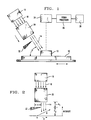
- FIG. 1 is a side view of a substrate 10 (e.g., a circuit board) having at least one raised, light-reflective topological feature 12 on the board surface, such as a solder paste deposit, or an active or passive surface mount component.
- a substrate 10 e.g., a circuit board
- a solder paste deposit e.g., a solder paste deposit
- an active or passive surface mount component e.g., an inspection is usually coupled out to assure that none of the features 12 are missing or mis- positioned.
- the feature 12 is a solder paste deposit, it is far less costly to reprint the deposits, should any be found to be missing or misplaced, rather than to wait until after the placement of components on the circuit board.
- Automated inspection of the substrate 10 using a conventional machine vision system is fraught with the difficulty that the surface of the feature 12 may be diffuse, as is often the case with solder paste deposits and with a large majority of active and passive components.
- the light reflected vertically upward from feature 12 is often not significantly brighter than that reflected from the surface of the substrate 10 surrounding the feature.
- the lack of contrast between the feature 12 and the area on the substrate 10 surrounding it makes detection of defects difficult.
- Such enhancement may be accomplished, in accordance with my invention, by directing a line of light 14, having a gradient intensity profile, at the feature 12 at an angle 0 relative to the surface of the substrate 10. It is important that the line of light 14, whose longitudinal axis extends into the plane of the drawing, have a gradient profile, that is, an intensity which decreases linearly along the zaxis. Referring both to FIGS.
- the line of light 14 is generated by a light source 16, typically, a well-controlled mercury or halogen lamp, whose light rays 18 are directed into a circle-to-line converter 20, typically a fiber optic bundle, which transform the rays 18 into the line of light 14 such that the longitudinal axis of the line extends into the plane of the drawing.
- a generally opaque wedge 22 is placed in front of the circle-to-line converter 22 to partially obstruct the line of line 14 so as to advantageously alter its profile (intensity) so that it is no longer constant but now has a linear gradient.
- the wedge 22 When placed in front of the circle-toline converter 20, the wedge 22, which is opaque, partially obstructs the line 14 so that at a point A directly underneath the wedge, no light is received. Conversely, at a point B which lies in the same plane as, but is laterally spaced from, the point A, all of the light from the line of light 14 is received. Within the region between the points A and B, the wedge 22 will obstruct the line of light 14 by creating a shadow in which there is not a sharp transition between light and dark, but rather a more gradual transition.
- the profile of the light illuminating the region between A and B will have a linear gradient.
- Equation (1) can be re-written as:
- the gradient of line of light 14 produced by placing the wedge 22 in front of the circle-to-line converter 20 can be controlled by varying the ratio between h 1 to h 2 . Note that it is possible to place the wedge 22 and the circle-to-line converter 20 as close as possible to the feature 12.
- the intensity 1 of light reflected vertically upwardly will vary in accordance with the height (z axis position) of the reflecting surface, assuming the reflectivity the substrate is everywhere equal. If the gradient profile of the line of light 14 is assumed to be linear, then the reflectance intensity can be given by the relationship: where a, b and k are constants.
- the reflecting surface height (Z) varies along the x axis of the substrate 10 because of the presence of the feature 12.
- the reflecting surface height can be given by:
- the resultant reflectivity intensity obtained by directing the gradient-profile line of light 14 at the substrate 10 will be greater in the region of the feature 12, owing to its greater height, than in the region surrounding to the feature which is typically of a lower height.
- the increase in the reflectance intensity attributed to the feature as a consequence of the use of a gradient-profile beam serves to enhance the contrast between the feature and the substrate.
- the image of the substrate 10 and the feature 12 is captured with the aid of a linescan camera 24 of a type well known in the art which serves to image a thin strip of area on the substrate running along the y axis parallel to the line of light 14.
- the output of the camera 24 is coupled to a vision processor 26 identical to the vision processor described in the aforementioned '410 patent.
- the vision processor 26 serves to process the output signal of the camera 24 to initially winnow the data so that only the image data representative of predetermined regions of interest within the strip imaged by the camera is retained. The retained image data is then processed by the vision processor 26 to determine the intensity of the light reflected from the regions of interest within the strip imaged by the linescan camera 24.
- a monitor 28 is coupled to the vision processor 24 for displaying reflectance intensity information from the processor.
- the linescan camera advantageously serves to capture the image of a thin strip of area running along the yaxis.
- the strip which is imaged thereby can be made to coincide with the strip illuminated by the gradient profile beam of light 14. In this way, the gradient profile of the illumination of the imaged strip will be well defined.
- the use of a two-dimensional array-type camera, in place of the linescan camera 24, would require strongly limiting the allowed gradient (and with it the image enhancement capabilities) in order to avoid camera saturation on one side of the image and a very dull image on the other.
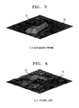
- FIG. 3 is an image of the substrate 10 and the feature 12 thereon, as captured by the camera 24 and processed by the image processor 24, when the substrate and feature are spanned by the camera and the line of light 14.
- FIG. 4 is an image of the substrate 10 and the feature 12 thereon, as captured by the camera 22 and processed by the image processor 24, when the substrate and feature are spanned by the camera and a line of light having a substantially uniform intensity profile.
- the contrast between the feature 12 and the surrounding area on the substrate 10 surrounding the feature in FIG. 3 is much greater.
- the contrast between the feature 12 and line area on the substrate 10 surrounding the feature is not very high, making it difficult to distinguish between the feature and the surrounding substrate area.
- the foregoing discloses a technique for enhancing the contrast between a light-reflective topological feature and its surrounding background within a captured image by illuminating the feature and its surrounding image with light having a gradient profile.
Landscapes
- Engineering & Computer Science (AREA)
- Physics & Mathematics (AREA)
- General Physics & Mathematics (AREA)
- Health & Medical Sciences (AREA)
- General Health & Medical Sciences (AREA)
- Multimedia (AREA)
- Theoretical Computer Science (AREA)
- Analytical Chemistry (AREA)
- Pathology (AREA)
- Chemical & Material Sciences (AREA)
- Computer Vision & Pattern Recognition (AREA)
- Biochemistry (AREA)
- Artificial Intelligence (AREA)
- Immunology (AREA)
- Life Sciences & Earth Sciences (AREA)
- Vascular Medicine (AREA)
- Length Measuring Devices By Optical Means (AREA)
- Investigating Materials By The Use Of Optical Means Adapted For Particular Applications (AREA)
- Image Processing (AREA)
- Image Analysis (AREA)
- Image Input (AREA)
- Supply And Installment Of Electrical Components (AREA)
Abstract
Description
- This invention relates to a method and apparatus for achieving an enhanced two-dimensional image of an object such that the object is contrasted from its surrounding background.
- Machine vision technology is now being employed in many industries for the purpose of rapidly accomplishing inspection of articles with very high accuracy. Within the electronics industry, machine vision systems are currently being employed to inspect populated circuit boards prior to soldering to detect missing and misplaced components as well as to inspect unpopulated boards prior to component placement to detect missing and misplaced solder paste deposits. In U.S. Patent 4,811,410, issued on March 7, 1989, in the names of I. Amir et al. (herein incorporated by reference), there is disclosed a circuit board inspection system comprised of a light source for illuminating a strip of area running across the surface of the board with light of substantially constant intensity. A linescan camera is provided for detecting the intensity of the light reflected from the illuminated strip. The output signal of the camera is processed by a vision system which initially serves to winnow the data so that only the data representing the image of predetermined regions of interest in the strip (where defects are more likely) is retained. The retained data is then processed to detect the presence of defects, if any, in the strip. By simultaneously spanning the circuit board with the light source and the camera, the entire surface of the board can thus be inspected for defects.
- While the Amir et al. vision system has proven itself capable of detecting defects such as missing and misplaced components and solder paste deposits, a lack of contrast between the features on the board (i.e., the components and/or solder paste deposits) can adversely affect the accuracy of inspection which is also the case for other conventional inspection systems. Often, the features of interest on the circuit board have a very low contrast with respect to the background and, as a consequence, the intensity of the light reflected from such features is often not appreciably greater than the light reflected from the board itself. Because the contrast between the circuit board and the features of interest is usually not very high, defect detection is difficult.
- Thus, there is a need for an improved two-dimensional imaging technique which advantageously enhances the boundary region between an object and its surrounding background to facilitate detection of the presence and position of the object.
- Briefly, in accordance with a preferred embodiment of the invention, a technique is disclosed for obtaining a two-dimensional image of a raised light-reflective topological feature (i.e., a component or a solder deposit) having a greater reflectivity than that of its surrounding, lower height background, to enhance the contrast between the feature and the background. The method is coupled out by first illuminating the feature and its surrounding background with a gradient-profile light beam directed thereat at an angle. The intensity of the beam decreases laterally between the beam edges, and therefore the beam is said to have a gradient profile. By illuminating the feature with an angularly-directed gradient-profile beam, the intensity of the light reflected upward by the feature and its surrounding area will be proportional to the height of the feature or surrounding area from which such light is reflected. The image of the feature and its surrounding area illuminated by the gradient-profile beam are captured with an image-acquisition device (e.g., a linescan camera) positioned directly there- above. The captured image is processed by a vision system which serves to determine the reflectance intensity associated with the feature and its surrounding background. If we assume that the surface reflectance is not much different from the object (otherwise good contrast will be achieved in any event), then the reflectance intensity will be proportional to the height of the feature and surrounding area and a higher reflectance intensity will be associated with the feature than its surrounding background because the feature is presumed to be at a greater height. In this way, the contrast between the feature and its surrounding area is enhanced. Likewise, if the feature is lower, the feature will look duller than its surrounding.
-
- FIG. 1 is a simplified view of a substrate, showing the manner in which the image of a topological feature on the substrate may be may be enhanced by the technique of the present invention;
- FIG. 2 is a schematic view of a mechanism for generating a gradient profile line of light for enhancing the image in the manner taught in FIG. 1;
- FIG. 3 is a representation of the image of the substrate of FIG. 1 obtained by the enhancement technique of the present invention; and.
- FIG. 4 is a representation of the image of the substrate of FIG. 1 obtained by a conventional two-dimensional imaging system.
- FIG. 1 is a side view of a substrate 10 (e.g., a circuit board) having at least one raised, light-reflective
topological feature 12 on the board surface, such as a solder paste deposit, or an active or passive surface mount component. In the course of fabricating thesubstrate 10, an inspection is usually coupled out to assure that none of thefeatures 12 are missing or mis- positioned. In the event that thefeature 12 is a solder paste deposit, it is far less costly to reprint the deposits, should any be found to be missing or misplaced, rather than to wait until after the placement of components on the circuit board. By the same token, it is far less costly to detect missing or misplaced components prior to solder-bonding to the circuit board than afterwards. - Automated inspection of the
substrate 10 using a conventional machine vision system, such as the one described in the aforementioned '410 patent, is fraught with the difficulty that the surface of thefeature 12 may be diffuse, as is often the case with solder paste deposits and with a large majority of active and passive components. The light reflected vertically upward fromfeature 12 is often not significantly brighter than that reflected from the surface of thesubstrate 10 surrounding the feature. The lack of contrast between thefeature 12 and the area on thesubstrate 10 surrounding it makes detection of defects difficult. - To overcome this difficulty, I have developed a novel technique which advantageously serves to enhance the contrast between the raised, light-reflective
topological feature 12 and thesubstrate 10. Such enhancement may be accomplished, in accordance with my invention, by directing a line of light 14, having a gradient intensity profile, at thefeature 12 at an angle 0 relative to the surface of thesubstrate 10. It is important that the line of light 14, whose longitudinal axis extends into the plane of the drawing, have a gradient profile, that is, an intensity which decreases linearly along the zaxis. Referring both to FIGS. 2 and 3, the line of light 14 is generated by alight source 16, typically, a well-controlled mercury or halogen lamp, whoselight rays 18 are directed into a circle-to-line converter 20, typically a fiber optic bundle, which transform therays 18 into the line of light 14 such that the longitudinal axis of the line extends into the plane of the drawing. A generallyopaque wedge 22 is placed in front of the circle-to-line converter 22 to partially obstruct the line of line 14 so as to advantageously alter its profile (intensity) so that it is no longer constant but now has a linear gradient. - To understand how the profile of the line of light 14 is altered by the
wedge 22, reference should be had to FIG. 2. When placed in front of the circle-toline converter 20, thewedge 22, which is opaque, partially obstructs the line 14 so that at a point A directly underneath the wedge, no light is received. Conversely, at a point B which lies in the same plane as, but is laterally spaced from, the point A, all of the light from the line of light 14 is received. Within the region between the points A and B, thewedge 22 will obstruct the line of light 14 by creating a shadow in which there is not a sharp transition between light and dark, but rather a more gradual transition. If, in the absence of thewedge 22, the light illuminabng the region between A and B would be of uniform intensity (which would be true if the distance between the points A and B is small), then when the wedge is placed in front of the circle-to-line converter 20, the profile of the light illuminating the region between A and B will have a linear gradient. - Assuming that the light striking the region between A and B is uniform in its illumination, the intensity 1 at any point z in mis region will be given by the relationship:

where Imax is the maximum illumination intensity. Equation (1) can be re-written as: -


then substituting eq.(3) into eq.(2) yields -

- Thus, the gradient of line of light 14 produced by placing the
wedge 22 in front of the circle-to-line converter 20 can be controlled by varying the ratio between h1 to h2. Note that it is possible to place thewedge 22 and the circle-to-line converter 20 as close as possible to thefeature 12. - When the gradient-profile line of light 14 is directed at an acute angle at the
substrate 10, the intensity 1 of light reflected vertically upwardly will vary in accordance with the height (z axis position) of the reflecting surface, assuming the reflectivity the substrate is everywhere equal. If the gradient profile of the line of light 14 is assumed to be linear, then the reflectance intensity can be given by the relationship:
where a, b and k are constants. - The reflecting surface height (Z) varies along the x axis of the
substrate 10 because of the presence of thefeature 12. Under the conditions depicted in FIG. 1 where thefeature 12 is presumed to line between the coordinates 0 and xo, the reflecting surface height can be given by:
where
- Combining eq. (5) and (6) yields.
-

substrate 10 will be greater in the region of thefeature 12, owing to its greater height, than in the region surrounding to the feature which is typically of a lower height. The increase in the reflectance intensity attributed to the feature as a consequence of the use of a gradient-profile beam serves to enhance the contrast between the feature and the substrate. - Referring to FIG. 1, in a preferred embodiment, the image of the
substrate 10 and thefeature 12 is captured with the aid of alinescan camera 24 of a type well known in the art which serves to image a thin strip of area on the substrate running along the y axis parallel to the line of light 14. The output of thecamera 24 is coupled to avision processor 26 identical to the vision processor described in the aforementioned '410 patent. Thevision processor 26 serves to process the output signal of thecamera 24 to initially winnow the data so that only the image data representative of predetermined regions of interest within the strip imaged by the camera is retained. The retained image data is then processed by thevision processor 26 to determine the intensity of the light reflected from the regions of interest within the strip imaged by thelinescan camera 24. Amonitor 28 is coupled to thevision processor 24 for displaying reflectance intensity information from the processor. To obtain an image of the entire surface of thesubstrate 10, it is necessary to span or sweep the substrate with the line of light 14 and thecamera 24. Typically, this is accomplished by displacing thesubstrate 10 along the x-axis with the aid of an x-axis slide 30. - There is a distinct advantage to imaging the substrate with a
linescan camera 24 because the linescan camera advantageously serves to capture the image of a thin strip of area running along the yaxis. By prop- edy positioning thelinescan camera 24, the strip which is imaged thereby can be made to coincide with the strip illuminated by the gradient profile beam of light 14. In this way, the gradient profile of the illumination of the imaged strip will be well defined. In contrast, the use of a two-dimensional array-type camera, in place of thelinescan camera 24, would require strongly limiting the allowed gradient (and with it the image enhancement capabilities) in order to avoid camera saturation on one side of the image and a very dull image on the other. - FIG. 3 is an image of the
substrate 10 and thefeature 12 thereon, as captured by thecamera 24 and processed by theimage processor 24, when the substrate and feature are spanned by the camera and the line of light 14. By contrast, FIG. 4 is an image of thesubstrate 10 and thefeature 12 thereon, as captured by thecamera 22 and processed by theimage processor 24, when the substrate and feature are spanned by the camera and a line of light having a substantially uniform intensity profile. As compared to FIG. 4, the contrast between thefeature 12 and the surrounding area on thesubstrate 10 surrounding the feature in FIG. 3 is much greater. In fact, as seen in FIG. 4, the contrast between thefeature 12 and line area on thesubstrate 10 surrounding the feature is not very high, making it difficult to distinguish between the feature and the surrounding substrate area. - The foregoing discloses a technique for enhancing the contrast between a light-reflective topological feature and its surrounding background within a captured image by illuminating the feature and its surrounding image with light having a gradient profile.
- It is to be understood that the above-described embodiments are merely illustrative of the principles of the invention. Various modifications and changes may be made thereto by those skilled in the art which will embody the principles of the invention and fall within the spirit and scope thereof.
Claims (6)
Applications Claiming Priority (2)
| Application Number | Priority Date | Filing Date | Title |
|---|---|---|---|
| US662583 | 1984-10-19 | ||
| US07/662,583 US5097516A (en) | 1991-02-28 | 1991-02-28 | Technique for illuminating a surface with a gradient intensity line of light to achieve enhanced two-dimensional imaging |
Publications (3)
| Publication Number | Publication Date |
|---|---|
| EP0501683A2 true EP0501683A2 (en) | 1992-09-02 |
| EP0501683A3 EP0501683A3 (en) | 1994-10-12 |
| EP0501683B1 EP0501683B1 (en) | 2001-12-12 |
Family
ID=24658312
Family Applications (1)
| Application Number | Title | Priority Date | Filing Date |
|---|---|---|---|
| EP92301435A Expired - Lifetime EP0501683B1 (en) | 1991-02-28 | 1992-02-21 | Technique for enhanced two-dimensional imaging |
Country Status (4)
| Country | Link |
|---|---|
| US (1) | US5097516A (en) |
| EP (1) | EP0501683B1 (en) |
| JP (1) | JPH07113966B2 (en) |
| DE (1) | DE69232279T2 (en) |
Cited By (1)
| Publication number | Priority date | Publication date | Assignee | Title |
|---|---|---|---|---|
| EP1079420A2 (en) * | 1999-08-27 | 2001-02-28 | Shinko Electric Industries Co. Ltd. | Inspection apparatus |
Families Citing this family (79)
| Publication number | Priority date | Publication date | Assignee | Title |
|---|---|---|---|---|
| US6115491A (en) * | 1996-02-27 | 2000-09-05 | Cyberoptics Corporation | Apparatus and method for estimating background tilt and offset |
| US6049384A (en) * | 1996-02-27 | 2000-04-11 | Cyberoptics Corporation | Method and apparatus for three dimensional imaging using multi-phased structured light |
| US5920735A (en) * | 1997-01-16 | 1999-07-06 | Gelphman; Janet L. | Method and apparatus to observe the geometry of relative motion |
| US6236747B1 (en) | 1997-02-26 | 2001-05-22 | Acuity Imaging, Llc | System and method for image subtraction for ball and bumped grid array inspection |
| US5828449A (en) * | 1997-02-26 | 1998-10-27 | Acuity Imaging, Llc | Ring illumination reflective elements on a generally planar surface |
| US5943125A (en) * | 1997-02-26 | 1999-08-24 | Acuity Imaging, Llc | Ring illumination apparatus for illuminating reflective elements on a generally planar surface |
| US6118524A (en) * | 1997-02-26 | 2000-09-12 | Acuity Imaging, Llc | Arc illumination apparatus and method |
| US6201892B1 (en) | 1997-02-26 | 2001-03-13 | Acuity Imaging, Llc | System and method for arithmetic operations for electronic package inspection |
| US5926557A (en) * | 1997-02-26 | 1999-07-20 | Acuity Imaging, Llc | Inspection method |
| JPH11220298A (en) * | 1998-02-02 | 1999-08-10 | Matsushita Electric Ind Co Ltd | Electronic component mounting method |
| US6148113A (en) * | 1998-02-03 | 2000-11-14 | Micrografx, Inc. | System for stimulating the depth of field of an image in two dimensional space and method of operation |
| US6262803B1 (en) * | 1998-09-10 | 2001-07-17 | Acuity Imaging, Llc | System and method for three-dimensional inspection using patterned light projection |
| US6768812B1 (en) * | 1999-05-27 | 2004-07-27 | Cognex Corporation | Method for locating features on an object using varied illumination |
| JP4052498B2 (en) | 1999-10-29 | 2008-02-27 | 株式会社リコー | Coordinate input apparatus and method |
| JP2001184161A (en) | 1999-12-27 | 2001-07-06 | Ricoh Co Ltd | Method and device for inputting information, writing input device, method for managing written data, method for controlling display, portable electronic writing device, and recording medium |
| US6803906B1 (en) | 2000-07-05 | 2004-10-12 | Smart Technologies, Inc. | Passive touch system and method of detecting user input |
| ES2279823T3 (en) * | 2000-07-05 | 2007-09-01 | Smart Technologies Inc. | TACTILE SYSTEM BASED ON CAMERAS. |
| SE518640C2 (en) * | 2000-07-11 | 2002-11-05 | Mydata Automation Ab | Method, apparatus for applying a viscous medium to a substrate, apparatus for applying additional viscous medium and the use of screen printing |
| US20020015103A1 (en) * | 2000-07-25 | 2002-02-07 | Zhimin Shi | System and method of capturing and processing digital images with depth channel |
| JP3858571B2 (en) * | 2000-07-27 | 2006-12-13 | 株式会社日立製作所 | Pattern defect inspection method and apparatus |
| US7058204B2 (en) * | 2000-10-03 | 2006-06-06 | Gesturetek, Inc. | Multiple camera control system |
| US6650422B2 (en) * | 2001-03-26 | 2003-11-18 | Advanced Micro Devices, Inc. | Scatterometry techniques to ascertain asymmetry profile of features and generate a feedback or feedforward process control data associated therewith |
| US20040001144A1 (en) | 2002-06-27 | 2004-01-01 | Mccharles Randy | Synchronization of camera images in camera-based touch system to enhance position determination of fast moving objects |
| US6954197B2 (en) * | 2002-11-15 | 2005-10-11 | Smart Technologies Inc. | Size/scale and orientation determination of a pointer in a camera-based touch system |
| US8456447B2 (en) | 2003-02-14 | 2013-06-04 | Next Holdings Limited | Touch screen signal processing |
| US8508508B2 (en) * | 2003-02-14 | 2013-08-13 | Next Holdings Limited | Touch screen signal processing with single-point calibration |
| US7629967B2 (en) | 2003-02-14 | 2009-12-08 | Next Holdings Limited | Touch screen signal processing |
| US6710890B1 (en) * | 2003-02-26 | 2004-03-23 | Kla-Tencor Technologies Corporation | Substrate thickness determination |
| US7532206B2 (en) | 2003-03-11 | 2009-05-12 | Smart Technologies Ulc | System and method for differentiating between pointers used to contact touch surface |
| US7352892B2 (en) * | 2003-03-20 | 2008-04-01 | Micron Technology, Inc. | System and method for shape reconstruction from optical images |
| US20040184653A1 (en) * | 2003-03-20 | 2004-09-23 | Baer Richard L. | Optical inspection system, illumination apparatus and method for use in imaging specular objects based on illumination gradients |
| US7256772B2 (en) | 2003-04-08 | 2007-08-14 | Smart Technologies, Inc. | Auto-aligning touch system and method |
| US7411575B2 (en) | 2003-09-16 | 2008-08-12 | Smart Technologies Ulc | Gesture recognition method and touch system incorporating the same |
| US7274356B2 (en) | 2003-10-09 | 2007-09-25 | Smart Technologies Inc. | Apparatus for determining the location of a pointer within a region of interest |
| US7355593B2 (en) | 2004-01-02 | 2008-04-08 | Smart Technologies, Inc. | Pointer tracking across multiple overlapping coordinate input sub-regions defining a generally contiguous input region |
| US7232986B2 (en) * | 2004-02-17 | 2007-06-19 | Smart Technologies Inc. | Apparatus for detecting a pointer within a region of interest |
| US7460110B2 (en) | 2004-04-29 | 2008-12-02 | Smart Technologies Ulc | Dual mode touch system |
| US7492357B2 (en) * | 2004-05-05 | 2009-02-17 | Smart Technologies Ulc | Apparatus and method for detecting a pointer relative to a touch surface |
| US7538759B2 (en) | 2004-05-07 | 2009-05-26 | Next Holdings Limited | Touch panel display system with illumination and detection provided from a single edge |
| US8120596B2 (en) | 2004-05-21 | 2012-02-21 | Smart Technologies Ulc | Tiled touch system |
| US7234456B2 (en) * | 2004-10-14 | 2007-06-26 | Kee Action Sports | Device for feeding balls into the ball chamber of a handgun |
| US7428899B2 (en) * | 2004-10-14 | 2008-09-30 | Kee Action Sports I Llc | Device for storing projectile balls and feeding them into the projectile chamber of a gun |
| US20070017495A1 (en) * | 2004-10-14 | 2007-01-25 | Heddies Andresen | Procedure and device for feeding balls into the projectile chamber of a handgun |
| JP4353100B2 (en) * | 2005-01-21 | 2009-10-28 | パナソニック株式会社 | Electronic component mounting system and electronic component mounting method |
| WO2007033309A2 (en) * | 2005-09-13 | 2007-03-22 | National Paintball Supply, Inc. | Clutch and detection means for paintball marker loader |
| CA2625223A1 (en) * | 2005-10-06 | 2007-04-19 | Kee Action Sports I Llc | Self-regulation paintball agitator system |
| WO2007044822A2 (en) * | 2005-10-11 | 2007-04-19 | Kee Action Sports I Llc | Magnetic drive bypass system for paintball loader |
| US20070165007A1 (en) * | 2006-01-13 | 2007-07-19 | Gerald Morrison | Interactive input system |
| US20070205994A1 (en) * | 2006-03-02 | 2007-09-06 | Taco Van Ieperen | Touch system and method for interacting with the same |
| US9442607B2 (en) | 2006-12-04 | 2016-09-13 | Smart Technologies Inc. | Interactive input system and method |
| WO2008128096A2 (en) * | 2007-04-11 | 2008-10-23 | Next Holdings, Inc. | Touch screen system with hover and click input methods |
| US8094137B2 (en) | 2007-07-23 | 2012-01-10 | Smart Technologies Ulc | System and method of detecting contact on a display |
| WO2009029764A1 (en) * | 2007-08-30 | 2009-03-05 | Next Holdings, Inc. | Low profile touch panel systems |
| KR20100055516A (en) * | 2007-08-30 | 2010-05-26 | 넥스트 홀딩스 인코포레이티드 | Optical touchscreen with improved illumination |
| US8405636B2 (en) * | 2008-01-07 | 2013-03-26 | Next Holdings Limited | Optical position sensing system and optical position sensor assembly |
| US20090207144A1 (en) * | 2008-01-07 | 2009-08-20 | Next Holdings Limited | Position Sensing System With Edge Positioning Enhancement |
| US20090213093A1 (en) * | 2008-01-07 | 2009-08-27 | Next Holdings Limited | Optical position sensor using retroreflection |
| WO2009137355A2 (en) * | 2008-05-06 | 2009-11-12 | Next Holdings, Inc. | Systems and methods for resolving multitouch scenarios using software filters |
| US20090277697A1 (en) * | 2008-05-09 | 2009-11-12 | Smart Technologies Ulc | Interactive Input System And Pen Tool Therefor |
| US8902193B2 (en) * | 2008-05-09 | 2014-12-02 | Smart Technologies Ulc | Interactive input system and bezel therefor |
| US20090278794A1 (en) * | 2008-05-09 | 2009-11-12 | Smart Technologies Ulc | Interactive Input System With Controlled Lighting |
| US20100079385A1 (en) * | 2008-09-29 | 2010-04-01 | Smart Technologies Ulc | Method for calibrating an interactive input system and interactive input system executing the calibration method |
| US20110205189A1 (en) * | 2008-10-02 | 2011-08-25 | John David Newton | Stereo Optical Sensors for Resolving Multi-Touch in a Touch Detection System |
| US8339378B2 (en) * | 2008-11-05 | 2012-12-25 | Smart Technologies Ulc | Interactive input system with multi-angle reflector |
| US20100225588A1 (en) * | 2009-01-21 | 2010-09-09 | Next Holdings Limited | Methods And Systems For Optical Detection Of Gestures |
| US20100229090A1 (en) * | 2009-03-05 | 2010-09-09 | Next Holdings Limited | Systems and Methods for Interacting With Touch Displays Using Single-Touch and Multi-Touch Gestures |
| US8692768B2 (en) | 2009-07-10 | 2014-04-08 | Smart Technologies Ulc | Interactive input system |
| US20110095977A1 (en) * | 2009-10-23 | 2011-04-28 | Smart Technologies Ulc | Interactive input system incorporating multi-angle reflecting structure |
| JP5525798B2 (en) * | 2009-11-20 | 2014-06-18 | 株式会社ニューフレアテクノロジー | Charged particle beam drawing apparatus and method for correcting charging effect thereof |
| US20110221666A1 (en) * | 2009-11-24 | 2011-09-15 | Not Yet Assigned | Methods and Apparatus For Gesture Recognition Mode Control |
| US20110199387A1 (en) * | 2009-11-24 | 2011-08-18 | John David Newton | Activating Features on an Imaging Device Based on Manipulations |
| US20110205186A1 (en) * | 2009-12-04 | 2011-08-25 | John David Newton | Imaging Methods and Systems for Position Detection |
| US20110193969A1 (en) * | 2010-02-09 | 2011-08-11 | Qisda Corporation | Object-detecting system and method by use of non-coincident fields of light |
| US20110234542A1 (en) * | 2010-03-26 | 2011-09-29 | Paul Marson | Methods and Systems Utilizing Multiple Wavelengths for Position Detection |
| US8428338B1 (en) | 2011-03-14 | 2013-04-23 | Panasonic Corporation | Method of determining solder paste height and device for determining solder paste height |
| DE102011056611A1 (en) | 2011-12-19 | 2013-06-20 | Taurus Instruments Gmbh | Method for determining a particle property and for classifying a particle charge and device for carrying out the method |
| US20190116863A1 (en) | 2017-10-24 | 2019-04-25 | Rai Strategic Holdings, Inc. | Method for formulating aerosol precursor for aerosol delivery device |
| US10527557B2 (en) * | 2017-12-29 | 2020-01-07 | Radiant Vision Systems, LLC | Adaptive diffuse illumination systems and methods |
| TWI689869B (en) * | 2018-12-28 | 2020-04-01 | 致茂電子股份有限公司 | Image inspection method |
Citations (3)
| Publication number | Priority date | Publication date | Assignee | Title |
|---|---|---|---|---|
| US4533245A (en) * | 1982-09-30 | 1985-08-06 | Milliken Research Corporation | Inspection lighting system |
| EP0252547A1 (en) * | 1986-07-11 | 1988-01-13 | Picanol N.V. | Method for controlling the location of the weft threads in a fabric |
| US4811410A (en) * | 1986-12-08 | 1989-03-07 | American Telephone And Telegraph Company | Linescan inspection system for circuit boards |
Family Cites Families (31)
| Publication number | Priority date | Publication date | Assignee | Title |
|---|---|---|---|---|
| US2446628A (en) * | 1947-03-06 | 1948-08-10 | Eastman Kodak Co | Flatness testing apparatus |
| US3069654A (en) * | 1960-03-25 | 1962-12-18 | Paul V C Hough | Method and means for recognizing complex patterns |
| US3695771A (en) * | 1970-08-06 | 1972-10-03 | Andras M Bardos | Method and apparatus for inspecting surfaces |
| US3692414A (en) * | 1971-02-24 | 1972-09-19 | Harry L Hosterman | Non-contacting measuring probe |
| JPS5418145B1 (en) * | 1971-06-08 | 1979-07-05 | ||
| JPS4839750A (en) * | 1971-09-15 | 1973-06-11 | ||
| US4009965A (en) * | 1972-05-15 | 1977-03-01 | Timothy Reed Pryor | Method and apparatus for determining object dimension and other characteristics using diffraction waves |
| US3962681A (en) * | 1972-06-19 | 1976-06-08 | Recognition Equipment Incorporated | Page width optical character processing method and system |
| US3877814A (en) * | 1973-02-07 | 1975-04-15 | Ppg Industries Inc | Method of and apparatus for detecting concave and convex portions in a specular surface |
| US4113389A (en) * | 1976-04-19 | 1978-09-12 | Morton Kaye | Optical measurement system |
| DE2630209C3 (en) * | 1976-07-05 | 1981-02-12 | Erwin Sick Gmbh Optik-Elektronik, 7808 Waldkirch | Electro-optical sensing device |
| US4139302A (en) * | 1977-02-17 | 1979-02-13 | Dr. Ralph M. Grant Engineering Consultants, Inc. | Method and apparatus for interferometric deformation analysis |
| US4240750A (en) * | 1978-10-02 | 1980-12-23 | Hurd William A | Automatic circuit board tester |
| US4295198A (en) * | 1979-04-02 | 1981-10-13 | Cogit Systems, Inc. | Automatic printed circuit dimensioning, routing and inspecting apparatus |
| US4379308A (en) * | 1980-02-25 | 1983-04-05 | Cooper Industries, Inc. | Apparatus for determining the parameters of figures on a surface |
| US4319843A (en) * | 1980-02-25 | 1982-03-16 | Burleigh Instruments, Inc. | Interferometer apparatus for the direct measurement of wavelength and frequency |
| US4473842A (en) * | 1981-07-06 | 1984-09-25 | Tokyo Shibaura Denki Kabushiki Kaisha | Apparatus and method for examining printed circuit board provided with electronic parts |
| JPS58142487A (en) * | 1982-02-18 | 1983-08-24 | Fuji Electric Co Ltd | Feature extracting device |
| JPS58156273A (en) * | 1982-03-11 | 1983-09-17 | Hajime Sangyo Kk | Masking device of picture information |
| US4545070A (en) * | 1982-04-30 | 1985-10-01 | Fuji Electric Company, Ltd. | Pattern discriminator |
| US4578810A (en) * | 1983-08-08 | 1986-03-25 | Itek Corporation | System for printed circuit board defect detection |
| JPS60200103A (en) * | 1984-03-26 | 1985-10-09 | Hitachi Ltd | Light cutting-plate line extraction circuit |
| EP0178090B1 (en) * | 1984-09-19 | 1990-11-22 | Ishida Scales Mfg. Co. Ltd. | Volume determination process |
| US4653104A (en) * | 1984-09-24 | 1987-03-24 | Westinghouse Electric Corp. | Optical three-dimensional digital data acquisition system |
| US4696047A (en) * | 1985-02-28 | 1987-09-22 | Texas Instruments Incorporated | Apparatus for automatically inspecting electrical connecting pins |
| DE3578241D1 (en) * | 1985-06-19 | 1990-07-19 | Ibm | METHOD FOR IDENTIFYING THREE-DIMENSIONAL OBJECTS BY MEANS OF TWO-DIMENSIONAL IMAGES. |
| JPS61293657A (en) * | 1985-06-21 | 1986-12-24 | Matsushita Electric Works Ltd | Method for inspecting soldering appearance |
| US4647208A (en) * | 1985-07-22 | 1987-03-03 | Perceptron, Inc. | Method for spatial measurement of holes |
| US4873651A (en) * | 1987-04-21 | 1989-10-10 | Case Western Reserve University | Method and apparatus for reconstructing three-dimensional surfaces from two-dimensional images |
| US4849645A (en) * | 1988-03-04 | 1989-07-18 | American Telephone And Telegraph Company | Substrate inspection system having two scattered light detecting bundles orthogonally positioned to each other |
| US4965665A (en) * | 1989-10-25 | 1990-10-23 | At&T Bell Laboratories | 3D imaging of a substrate using perpendicular scanning directions |
-
1991
- 1991-02-28 US US07/662,583 patent/US5097516A/en not_active Expired - Fee Related
-
1992
- 1992-02-21 EP EP92301435A patent/EP0501683B1/en not_active Expired - Lifetime
- 1992-02-21 DE DE69232279T patent/DE69232279T2/en not_active Expired - Fee Related
- 1992-02-24 JP JP4072195A patent/JPH07113966B2/en not_active Expired - Fee Related
Patent Citations (3)
| Publication number | Priority date | Publication date | Assignee | Title |
|---|---|---|---|---|
| US4533245A (en) * | 1982-09-30 | 1985-08-06 | Milliken Research Corporation | Inspection lighting system |
| EP0252547A1 (en) * | 1986-07-11 | 1988-01-13 | Picanol N.V. | Method for controlling the location of the weft threads in a fabric |
| US4811410A (en) * | 1986-12-08 | 1989-03-07 | American Telephone And Telegraph Company | Linescan inspection system for circuit boards |
Non-Patent Citations (1)
| Title |
|---|
| COMPUTER VISION, GRAPHICS, AND IMAGE PROCESSING, DEC. 1985, USA, VOL. 32, NR. 3, PAGE(S) 337 - 358, ISSN 0734-189X Carrihill B et al 'Experiments with the intensity ratio depth sensor' * |
Cited By (3)
| Publication number | Priority date | Publication date | Assignee | Title |
|---|---|---|---|---|
| EP1079420A2 (en) * | 1999-08-27 | 2001-02-28 | Shinko Electric Industries Co. Ltd. | Inspection apparatus |
| EP1079420A3 (en) * | 1999-08-27 | 2001-08-08 | Shinko Electric Industries Co. Ltd. | Inspection apparatus |
| US6738504B1 (en) | 1999-08-27 | 2004-05-18 | Shinko Electric Industries Co., Ltd | Inspection apparatus for semiconductor device and parts mounter using same |
Also Published As
| Publication number | Publication date |
|---|---|
| EP0501683B1 (en) | 2001-12-12 |
| JPH07113966B2 (en) | 1995-12-06 |
| EP0501683A3 (en) | 1994-10-12 |
| DE69232279T2 (en) | 2002-08-08 |
| JPH06168321A (en) | 1994-06-14 |
| DE69232279D1 (en) | 2002-01-24 |
| US5097516A (en) | 1992-03-17 |
Similar Documents
| Publication | Publication Date | Title |
|---|---|---|
| EP0501683A2 (en) | Technique for enhanced two-dimensional imaging | |
| JPH0572961B2 (en) | ||
| US7355692B2 (en) | System and method for inspecting electrical circuits utilizing reflective and fluorescent imagery | |
| US5101442A (en) | Three-dimensional imaging technique using sharp gradient of illumination | |
| US20130148116A1 (en) | Inspection system, inspection method, and program | |
| JPS58146844A (en) | Automatic optical characteristic inspecting device | |
| US7039228B1 (en) | System and method for three-dimensional surface inspection | |
| US5048965A (en) | Three-dimensional imaging technique with occlusion avoidance | |
| JP3170598B2 (en) | Appearance inspection device | |
| US20030117616A1 (en) | Wafer external inspection apparatus | |
| JP2001209798A (en) | Method and device for inspecting outward appearance | |
| JP2005098970A (en) | Method and apparatus for identifying foreign matter | |
| JP3262150B2 (en) | Inspection device for solder joints | |
| JP2007298526A (en) | Inspection apparatus, inspection method and manufacturing method of pattern substrate | |
| JP2002228592A (en) | Surface inspection device and surface scrutinizing device | |
| JPH04329344A (en) | Mounted board inspecting device | |
| JPH04142410A (en) | Shape recognizing device | |
| JP3366211B2 (en) | Mirror object imaging method | |
| JPS61193007A (en) | Inspecting method for rod type projection body | |
| JP3189604B2 (en) | Inspection method and device | |
| JPH0774724B2 (en) | Inspection method | |
| KR100275565B1 (en) | Apparatus for inspecting printed shape of solder paste on printed circuit board | |
| JPS638417B2 (en) | ||
| JPH08219740A (en) | Method and equipment for inspecting semiconductor device | |
| JP2002139440A (en) | Illuminator for pattern inspection |
Legal Events
| Date | Code | Title | Description |
|---|---|---|---|
| PUAI | Public reference made under article 153(3) epc to a published international application that has entered the european phase |
Free format text: ORIGINAL CODE: 0009012 |
|
| AK | Designated contracting states |
Kind code of ref document: A2 Designated state(s): DE FR GB IT |
|
| RAP3 | Party data changed (applicant data changed or rights of an application transferred) |
Owner name: AT&T CORP. |
|
| PUAL | Search report despatched |
Free format text: ORIGINAL CODE: 0009013 |
|
| AK | Designated contracting states |
Kind code of ref document: A3 Designated state(s): DE FR GB IT |
|
| 17P | Request for examination filed |
Effective date: 19950330 |
|
| 17Q | First examination report despatched |
Effective date: 19981223 |
|
| RIC1 | Information provided on ipc code assigned before grant |
Free format text: 7G 06K 9/20 A, 7G 01N 21/88 B |
|
| GRAG | Despatch of communication of intention to grant |
Free format text: ORIGINAL CODE: EPIDOS AGRA |
|
| GRAG | Despatch of communication of intention to grant |
Free format text: ORIGINAL CODE: EPIDOS AGRA |
|
| GRAG | Despatch of communication of intention to grant |
Free format text: ORIGINAL CODE: EPIDOS AGRA |
|
| GRAH | Despatch of communication of intention to grant a patent |
Free format text: ORIGINAL CODE: EPIDOS IGRA |
|
| GRAH | Despatch of communication of intention to grant a patent |
Free format text: ORIGINAL CODE: EPIDOS IGRA |
|
| GRAA | (expected) grant |
Free format text: ORIGINAL CODE: 0009210 |
|
| AK | Designated contracting states |
Kind code of ref document: B1 Designated state(s): DE FR GB IT |
|
| REG | Reference to a national code |
Ref country code: GB Ref legal event code: IF02 |
|
| REF | Corresponds to: |
Ref document number: 69232279 Country of ref document: DE Date of ref document: 20020124 |
|
| PGFP | Annual fee paid to national office [announced via postgrant information from national office to epo] |
Ref country code: DE Payment date: 20020328 Year of fee payment: 11 |
|
| PLBE | No opposition filed within time limit |
Free format text: ORIGINAL CODE: 0009261 |
|
| STAA | Information on the status of an ep patent application or granted ep patent |
Free format text: STATUS: NO OPPOSITION FILED WITHIN TIME LIMIT |
|
| 26N | No opposition filed | ||
| PGFP | Annual fee paid to national office [announced via postgrant information from national office to epo] |
Ref country code: FR Payment date: 20030122 Year of fee payment: 12 |
|
| PGFP | Annual fee paid to national office [announced via postgrant information from national office to epo] |
Ref country code: GB Payment date: 20030124 Year of fee payment: 12 |
|
| PG25 | Lapsed in a contracting state [announced via postgrant information from national office to epo] |
Ref country code: DE Free format text: LAPSE BECAUSE OF NON-PAYMENT OF DUE FEES Effective date: 20030902 |
|
| PG25 | Lapsed in a contracting state [announced via postgrant information from national office to epo] |
Ref country code: GB Free format text: LAPSE BECAUSE OF NON-PAYMENT OF DUE FEES Effective date: 20040221 |
|
| GBPC | Gb: european patent ceased through non-payment of renewal fee |
Effective date: 20040221 |
|
| PG25 | Lapsed in a contracting state [announced via postgrant information from national office to epo] |
Ref country code: FR Free format text: LAPSE BECAUSE OF NON-PAYMENT OF DUE FEES Effective date: 20041029 |
|
| REG | Reference to a national code |
Ref country code: FR Ref legal event code: ST |
|
| PG25 | Lapsed in a contracting state [announced via postgrant information from national office to epo] |
Ref country code: IT Free format text: LAPSE BECAUSE OF NON-PAYMENT OF DUE FEES;WARNING: LAPSES OF ITALIAN PATENTS WITH EFFECTIVE DATE BEFORE 2007 MAY HAVE OCCURRED AT ANY TIME BEFORE 2007. THE CORRECT EFFECTIVE DATE MAY BE DIFFERENT FROM THE ONE RECORDED. Effective date: 20050221 |