EP0501462A2 - Anzeigegerät - Google Patents
Anzeigegerät Download PDFInfo
- Publication number
- EP0501462A2 EP0501462A2 EP92103298A EP92103298A EP0501462A2 EP 0501462 A2 EP0501462 A2 EP 0501462A2 EP 92103298 A EP92103298 A EP 92103298A EP 92103298 A EP92103298 A EP 92103298A EP 0501462 A2 EP0501462 A2 EP 0501462A2
- Authority
- EP
- European Patent Office
- Prior art keywords
- signal
- screen
- video data
- display apparatus
- display
- Prior art date
- Legal status (The legal status is an assumption and is not a legal conclusion. Google has not performed a legal analysis and makes no representation as to the accuracy of the status listed.)
- Granted
Links
Images


Classifications
-
- H—ELECTRICITY
- H04—ELECTRIC COMMUNICATION TECHNIQUE
- H04N—PICTORIAL COMMUNICATION, e.g. TELEVISION
- H04N9/00—Details of colour television systems
- H04N9/12—Picture reproducers
- H04N9/30—Picture reproducers using solid-state colour display devices
-
- G—PHYSICS
- G09—EDUCATION; CRYPTOGRAPHY; DISPLAY; ADVERTISING; SEALS
- G09G—ARRANGEMENTS OR CIRCUITS FOR CONTROL OF INDICATING DEVICES USING STATIC MEANS TO PRESENT VARIABLE INFORMATION
- G09G3/00—Control arrangements or circuits, of interest only in connection with visual indicators other than cathode-ray tubes
- G09G3/20—Control arrangements or circuits, of interest only in connection with visual indicators other than cathode-ray tubes for presentation of an assembly of a number of characters, e.g. a page, by composing the assembly by combination of individual elements arranged in a matrix no fixed position being assigned to or needed to be assigned to the individual characters or partial characters
-
- H—ELECTRICITY
- H04—ELECTRIC COMMUNICATION TECHNIQUE
- H04N—PICTORIAL COMMUNICATION, e.g. TELEVISION
- H04N3/00—Scanning details of television systems; Combination thereof with generation of supply voltages
- H04N3/10—Scanning details of television systems; Combination thereof with generation of supply voltages by means not exclusively optical-mechanical
- H04N3/12—Scanning details of television systems; Combination thereof with generation of supply voltages by means not exclusively optical-mechanical by switched stationary formation of lamps, photocells or light relays
-
- H—ELECTRICITY
- H04—ELECTRIC COMMUNICATION TECHNIQUE
- H04N—PICTORIAL COMMUNICATION, e.g. TELEVISION
- H04N7/00—Television systems
- H04N7/01—Conversion of standards, e.g. involving analogue television standards or digital television standards processed at pixel level
- H04N7/0105—Conversion of standards, e.g. involving analogue television standards or digital television standards processed at pixel level using a storage device with different write and read speed
-
- G—PHYSICS
- G09—EDUCATION; CRYPTOGRAPHY; DISPLAY; ADVERTISING; SEALS
- G09G—ARRANGEMENTS OR CIRCUITS FOR CONTROL OF INDICATING DEVICES USING STATIC MEANS TO PRESENT VARIABLE INFORMATION
- G09G2340/00—Aspects of display data processing
- G09G2340/04—Changes in size, position or resolution of an image
- G09G2340/0407—Resolution change, inclusive of the use of different resolutions for different screen areas
-
- G—PHYSICS
- G09—EDUCATION; CRYPTOGRAPHY; DISPLAY; ADVERTISING; SEALS
- G09G—ARRANGEMENTS OR CIRCUITS FOR CONTROL OF INDICATING DEVICES USING STATIC MEANS TO PRESENT VARIABLE INFORMATION
- G09G2340/00—Aspects of display data processing
- G09G2340/12—Overlay of images, i.e. displayed pixel being the result of switching between the corresponding input pixels
- G09G2340/125—Overlay of images, i.e. displayed pixel being the result of switching between the corresponding input pixels wherein one of the images is motion video
Definitions
- This invention relates to a display apparatus in which a large number of display elements such as luminescence cells or cells for controlling the light intensity are arranged in a matrix form, and which displays images, characters, graphics or the like.
- Fig. 1 is a block diagram illustrating the configuration of a typical example of such a display apparatus which is disclosed in U.S. patent No. 4,498,081.
- an analog composite video signal 1 is inputted to a synchronizing separator circuit 2A.
- This synchronizing separator circuit 2A separates from the composite video signal 1 a horizontal synchronizing signal and a vertical synchronizing signal which are in turn supplied to a write control circuit 4.
- a chrominance demodulator circuit 2B independently separates luminance signals for red, green and blue from a separated video signal and outputs them in the form of analog signals to an A/D (analog to digital) converter 3.
- the A/D converter 3 generates a digital signal for each color in accordance with the corresponding luminance signal.
- a data multiplexer 5 which receives these digital signals selects one of them successively according to the color arrangement of cathode ray tubes 21 on a display board.
- the selected digital signals are transferred as the write data to a data latch circuit 6 as they are, and temporarily latched therein until the timing of writing data into a video data memory 8 occurs.
- the write control circuit 4 In accordance with the input synchronizing signal, the write control circuit 4 generates a signal for specifying an address in the video data memory 8, i.e., a memory write address signal, and sends it to an address multiplexer 7.
- the address multiplexer 7 receives a signal from a memory read and write controller 14 which is adapted to set the time sharing of the write period and the read period of each of the video data memory 8, a graphic data memory 9 and a blanking data memory 10, and in response to this signal sends the memory write address signal to the video data memory 8 only during the write period, thereby storing the latched write data into a desired address.
- the video data memory 8 comprises a RAM (random access memory) having memory elements the number of which corresponds to that of the cathode ray tubes 21 arranged in a matrix form on the display board.
- the data are written in positions corresponding to the respective memory write address signals.
- characters and graphics are displayed by using the graphic data memory 9 in correspondence to the video data memory 8, and characters or the like are displayed by blanking video signals from the video data memory 8 with data from the blanking data memory 10.
- a particular region of the display board is controlled by using a video mode memory 11, a graphic mode memory 12 and a blanking mode memory 13, so that, in one or more specified areas of the particular region, data from the video data memory 8, the graphic data memory 9 or the blanking data memory 10 are locked.
- Data from the video mode memory 11 are supplied through an OR circuit 31 to an inhibit terminal of an AND circuit 32, so that data from the video data memory 8 which correspond to an area set by a data processor 16 are locked to the video mode memory 11.
- Data from the graphic mode memory 12 are supplied to an inhibit terminal of an AND circuit 30, so that data from the graphic data memory 9 which correspond to an area set by the graphic mode memory 12 are locked.
- Data from the blanking mode memory 13 are supplied to an inhibit terminal of an AND circuit 29, so that data from the blanking data memory 10 which correspond to an area set by the blanking mode memory 13 are locked.
- Data read out from the video data memory 8, graphic data memory 9 and blanking data memory 10 are supplied through an OR circuit 33 to a data comparator 18.
- a display set and reset address generating circuit 15 receives a timing signal from the memory read and write controller 14, and generates an address signal for reading data from a memory which is in turn supplied to the address multiplexer 7. Upon receiving the timing signal from the memory read and write controller 14, the address multiplexer 7 opens its gate for a predetermined read period. In this operation, reading address signals are supplied to the video data memory 8, and the reading operation is carried out.
- reading address signals for each of the memories 9 and 10 are supplied in the same manner as the above at every predetermined read period to the address multiplexer 7.
- the display set and reset address generating circuit 15 supplies "on" discriminating comparison data for the cathode ray tube 21 to the data comparator 18.
- the data comparator 18 sequentially compares read-out data with the comparison data of each step, and outputs "on” and “off” signals to a data latch circuit 19 according to the levels of the read-out signals.
- column drive circuits 23 are driven to control the brightness of the cathode ray tubes 21. More specifically, a D-type flip-flop 20 is coupled to the cathode of each of the cathode ray tubes 21 through a transistor 22, and the output of the respective column drive circuit 23 is inputted to the data input terminals D of the flip-flops 20.
- the display set and reset address generating circuit 15 generates an address signal and a set signal, and the set signal is received by a set address discriminating circuit 24 corresponding to the address.
- the set signal is outputted from a line drive circuit 25 of the corresponding line to the terminals T of the flip-flops 20 which are coupled to the cathode ray tubes 21 in the corresponding line.
- these flip-flops 20 are set so that the corresponding cathode ray tubes 21 are turned on or off. Furthermore, the display set and reset address generating circuit 15 also generates an address signal and a reset signal, and the reset signal is received by a reset address discriminating circuit 26 corresponding to the address. The reset signal is outputted from a line drive circuit 27 of the corresponding line to the reset terminals of the flip-flops 20, thereby resetting these flip-flops 20.
- each cathode ray tube 21 corresponds to the data supplied from the data comparator 18.
- the brightness of the each cathode ray tube 21, i.e., the brightness of the entire screen of the display board can be controlled by changing the time interval between the generations of the two signals.
- Graphic data read out from the graphic data memory 9 are superposed on video data through the OR circuit 33, and graphics are displayed on the screen. Since data read out from the blanking data memory 10 are inputted to the inhibit terminal of the AND circuit 32 through the AND circuit 29 and OR circuit 31, video data are blanked in accordance with the blanking data.
- a horizontal display period is T H
- a vertical display period is T V
- the display apparatus comprises: a selection circuit for selecting one of a plurality of input video signals; a band-pass filter for limiting the selected video signal to a frequency band width equal to or narrower than the half of a frequency band which is calculated on the basis of the number of display elements along the horizontal direction of a screen; and a computing circuit for computing vertical interpolation video data in order to correct the difference between the number of display elements along the vertical direction and the number of scanning lines along the vertical direction of the selected video signal.
- the partial omission of reproducing video signals along the horizontal direction is prevented from occurring by the filtering effect of the band-pass filter. Furthermore, the partial omission of reproducing video signals along the vertical direction is prevented from occurring by displaying an image while controlling each display element of the screen in accordance with the computed vertical interpolation video data.
- Fig. 1 is a block diagram illustrating the configuration of a prior art display apparatus.
- Fig. 2 is a block diagram illustrating the configuration of a display apparatus according to the invention.
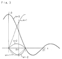
- Fig. 3 is a graph showing the characteristics of coefficient data for interpolation.
- Fig. 2 is a block diagram illustrating the configuration of a display apparatus according to the invention.
- 31 and 32 respectively indicate video signal input terminals to which a plurality of video signals are inputted, and composite synchronizing signal input terminals to which composite synchronizing signals corresponding to the video signals are inputted.
- Video signals are supplied through the input terminals 31 and an impedance matching circuit 33 to a signal switch circuit 34.
- One of the input video signals is selected by the signal switch circuit 34, and inputted to a band-pass filter 35.
- Composite synchronizing signals are supplied through the input terminals 32 and another impedance matching circuit 33 to another signal switch circuit 34.
- One of the input composite synchronizing signals is selected by the signal switch circuit 34, and inputted to an synchronizing separator circuit 47. These selections of input signals are controlled by an input controller 53.
- the band-pass filter 35 limits the input video signal to a frequency band width equal to or narrower than the half of a frequency calculated from the number (M) of display elements along the horizontal direction which are arranged in a matrix form on a screen 46, and then supplies the video signal to an A/D converter 36.
- the synchronizing separator circuit 47 separates the input composite synchronizing signal into a horizontal synchronizing signal H and a vertical synchronizing signal V.
- the horizontal synchronizing signal H is sent to a sampling signal generation circuit 48 and a computed data generation circuit 49.
- the vertical synchronizing signal V is supplied to the sampling signal generation circuit 48, the computed data generation circuit 49, a memory write control circuit 50 and a memory read control circuit 51.
- the sampling signal generation circuit 48 On the basis of data indicative of the horizontal display period (T H ) from the input controller 53 and the number M of display elements along the horizontal direction which has been previously set, the sampling signal generation circuit 48 generates a sampling pulse P H which is synchronized and coincident in phase with the horizontal synchronizing signal H and which has a frequency of M/T H .
- the sampling pulse P H is supplied to the A/D converter 36, a line memory 37, a data latch circuit 39, the computed data generation circuit 49, the memory write control circuit 50 and the memory read control circuit 51.
- the sampling signal generation circuit 48 Furthermore, on the basis of data indicative of the vertical display period (T V ) from the input controller 53 and the number (N) of display elements along the vertical direction of the screen 46 which has been previously set, the sampling signal generation circuit 48 also generates a pulse P V which is synchronized and coincident in phase with the vertical synchronizing signal V and which has a frequency of N/T V .
- the pulse P V is supplied to the computed data generation circuit 49, the memory write control circuit 50 and the memory read control circuit 51.
- the A/D converter 36 performs the A/D conversion against the input video signal at the timing of the sampling pulse P H , and the resulting digital video signal is supplied to the line memory 37.
- the line memory 37 temporarily stores input data.
- the combination of the line memory 37, the computed data generation circuit 49 and a computing circuit 38 conducts the interpolation computing in the manner described later.
- the computed result is temporarily stored by the data latch circuit 39.
- the memory write control circuit 50 generates a memory write address on the basis of the vertical synchronizing signal V, the pulse P V and the sampling pulse P H , and outputs it to an address switch circuit 41.
- the memory read control circuit 51 generates a memory read address on the basis of the vertical synchronizing signal V, the pulse P V and the sampling pulse P H , and outputs it to the address switch circuit 41.
- Video data from the data latch circuit 39 are written into a video memory 40 in accordance with the memory write address from the address switch circuit 41.
- Video data are read out from the video memory 40 in accordance with the memory read address from the address switch circuit 41, and the read out video data are sent to a comparison circuit 42.
- the comparison circuit 42 compares the video data read out from the video memory 40 with this weight data, and sends M number of data indicative of lighting or non-lighting to a data latch circuit 43 which in turn temporarily stores these data.
- the memory read control circuit 51 outputs a driving trigger pulse to a driving signal generation circuit 52.
- the driving signal generation circuit 52 supplies a driving voltage required for lighting to a line driving circuit 45 and a column driving circuit 44.
- the line and column driving circuits 45 and 44 control "on” and "off” of each of the M ⁇ N display elements of the screen 46.
- the signal switch circuits 34, 34 select one of the video signals and one of the composite synchronizing signals which corresponds to the selected video signal, under the control of the output of the input controller 53.
- the selected video signal is limited to the frequency band width equal to or narrower than the half of the signal band M/T H by the band-pass filter 35, and the video signal is then sent to the A/D converter 36.
- the selected composite synchronizing signal is sent to the synchronizing separator circuit 47, and separated therein into the horizontal synchronizing signal H and the vertical synchronizing signal V.
- the sampling signal generation circuit 48 generates the sampling pulse P H of a frequency of M/T H on the basis of the horizontal display period T H and the horizontal-display element number M, and also the pulse P V of a frequency of N/T V on the basis of the vertical display period T V and the vertical-display element number N.
- the video signal inputted to the A/D converter 36 is converted into a digital signal at the timing of the sampling pulse P H , and thereafter temporarily stored in the line memory 37 in the unit of one horizontal line to be used in the later vertical interpolation computing.
- time function I( ⁇ t) of time ⁇ t can be expressed as follows:
- the interpolation along the vertical direction is carried out by using this approximation expression.
- the computed data generation circuit 49 the time difference ⁇ t between the pulse P V and the vertical synchronizing signal V is obtained, and values respectively corresponding to those of k shown in Fig. 3 are obtained from this time difference ⁇ t and supplied to the computing circuit 38.
- interpolation video data are computed on the basis of these values and actual data for five lines of I(-2T), I(-T), I(0), I(T) and I(2T) which are stored in the line memory 37.
- the thus obtained interpolation video data are temporarily stored in the data latch circuit 39 until the timing of writing data into the video memory 40 occurs.
- the data stored in the data latch circuit 39 are written into the video memory 40 during the idle period of the memory read control circuit 51.
- the memory read control circuit 51 performs the driving process in the unit of line.
- the gradation control of the luminous strength is done by controlling the period and the lighting number of each display element.
- the gradation of the 1-bit weight can be achieved by switching one line on and off one time during the vertical display period T V .
- the M number of data for the line selected once in the period of T V /N are read out from the video memory 40, and the read out data are compared with the 1-bit weight data set in the comparison circuit 42. Then, the M number of data (one bit) indicative of lighting or non-lighting are temporarily stored in the data latch circuit 43.
- the memory read control circuit 51 supplies the driving trigger pulse to the driving signal generation circuit 52 which in turn supplies the driving voltage required for lighting to the line driving circuit 45 and the column driving circuit 44. This operation is conducted one time for every N lines during the vertical display period T V .
- the above-described embodiment is configured so as to process monochrome video signals.
- the circuitry from the impedance matching circuit 33 to the column driving circuit 44 is constructed in triplex.
- the interpolation computing is performed on the basis of data of five continuous lines. According to the invention, the interpolation computing may be performed on the basis of data obtained in another system, for example, data of two lines.
- the display elements used in the embodiment are of the luminous type, and driven by controlling their driving period or number.
- the display elements are driven by another driven system.
- the frequency band is limited on the basis of the screen display period of a signal selected by switching a plurality of video signals and the number of the display elements, and the interpolation computing along the vertical direction is performed.
- the display apparatus of the invention therefore, the abilities of a screen can be exhibited at the full, thereby allowing different kinds of video signals to be reproduced.
Landscapes
- Engineering & Computer Science (AREA)
- Multimedia (AREA)
- Signal Processing (AREA)
- Physics & Mathematics (AREA)
- Computer Hardware Design (AREA)
- General Physics & Mathematics (AREA)
- Theoretical Computer Science (AREA)
- Control Of Indicators Other Than Cathode Ray Tubes (AREA)
- Transforming Electric Information Into Light Information (AREA)
Applications Claiming Priority (2)
| Application Number | Priority Date | Filing Date | Title |
|---|---|---|---|
| JP58172/91 | 1991-02-28 | ||
| JP3058172A JP2790546B2 (ja) | 1991-02-28 | 1991-02-28 | 表示装置 |
Publications (3)
| Publication Number | Publication Date |
|---|---|
| EP0501462A2 true EP0501462A2 (de) | 1992-09-02 |
| EP0501462A3 EP0501462A3 (de) | 1992-09-23 |
| EP0501462B1 EP0501462B1 (de) | 1996-01-10 |
Family
ID=13076583
Family Applications (1)
| Application Number | Title | Priority Date | Filing Date |
|---|---|---|---|
| EP92103298A Expired - Lifetime EP0501462B1 (de) | 1991-02-28 | 1992-02-26 | Anzeigegerät |
Country Status (4)
| Country | Link |
|---|---|
| US (1) | US5235429A (de) |
| EP (1) | EP0501462B1 (de) |
| JP (1) | JP2790546B2 (de) |
| DE (1) | DE69207447T2 (de) |
Cited By (2)
| Publication number | Priority date | Publication date | Assignee | Title |
|---|---|---|---|---|
| FR2726723A1 (fr) * | 1994-11-08 | 1996-05-10 | Synelec Sa | Dispositif de retro-projection a frequence fixe d'images provenant de sources d'informations d'images possedant des frequences de balayage quelconques |
| WO1998052177A3 (en) * | 1997-05-16 | 1999-02-04 | Motorola Inc | Method and apparatus for driving a capacitive display device |
Families Citing this family (1)
| Publication number | Priority date | Publication date | Assignee | Title |
|---|---|---|---|---|
| US5768507A (en) * | 1995-09-29 | 1998-06-16 | Cirrus Logic, Inc. | Method and apparatus for overcoming a slope overload condition while using differential pulse code modulation scheme |
Family Cites Families (13)
| Publication number | Priority date | Publication date | Assignee | Title |
|---|---|---|---|---|
| JPS5331698Y2 (de) * | 1973-05-19 | 1978-08-07 | ||
| GB1512062A (en) * | 1974-05-13 | 1978-05-24 | Sony Corp | Colour video display apparatus |
| US4006298A (en) * | 1975-05-20 | 1977-02-01 | Gte Laboratories Incorporated | Bistable matrix television display system |
| JPS546421A (en) * | 1977-06-16 | 1979-01-18 | Sony Corp | Picture display unit |
| JPS558158A (en) * | 1978-07-04 | 1980-01-21 | Seiko Epson Corp | Display unit |
| JPS6153908B1 (de) * | 1980-07-25 | 1986-11-19 | Mitsubishi Electric Corp | |
| JPS61110198A (ja) * | 1984-11-05 | 1986-05-28 | 株式会社東芝 | マトリクス形表示装置 |
| JPS62145975A (ja) * | 1985-12-20 | 1987-06-30 | Casio Comput Co Ltd | 画像表示装置 |
| JPS62145974A (ja) * | 1985-12-20 | 1987-06-30 | Casio Comput Co Ltd | 画像表示方式 |
| JPS6411075U (de) * | 1987-07-09 | 1989-01-20 | ||
| JPH02179681A (ja) * | 1988-12-29 | 1990-07-12 | Daishinku Co | ドットマトリックス型表示媒体の制御装置 |
| DE3918007A1 (de) * | 1989-06-02 | 1990-12-06 | Grundig Emv | Schaltungsanordnung zur normwandlung von videosignalen fuer die darstellung an einem wiedergabegeraet mit einer matrixfoermigen anzeigeeinrichtung |
| US5166801A (en) * | 1989-11-22 | 1992-11-24 | Nec Corporation | Large size display apparatus for high definition television |
-
1991
- 1991-02-28 JP JP3058172A patent/JP2790546B2/ja not_active Expired - Lifetime
-
1992
- 1992-02-24 US US07/840,313 patent/US5235429A/en not_active Expired - Lifetime
- 1992-02-26 DE DE69207447T patent/DE69207447T2/de not_active Expired - Fee Related
- 1992-02-26 EP EP92103298A patent/EP0501462B1/de not_active Expired - Lifetime
Cited By (2)
| Publication number | Priority date | Publication date | Assignee | Title |
|---|---|---|---|---|
| FR2726723A1 (fr) * | 1994-11-08 | 1996-05-10 | Synelec Sa | Dispositif de retro-projection a frequence fixe d'images provenant de sources d'informations d'images possedant des frequences de balayage quelconques |
| WO1998052177A3 (en) * | 1997-05-16 | 1999-02-04 | Motorola Inc | Method and apparatus for driving a capacitive display device |
Also Published As
| Publication number | Publication date |
|---|---|
| US5235429A (en) | 1993-08-10 |
| DE69207447T2 (de) | 1996-05-23 |
| EP0501462A3 (de) | 1992-09-23 |
| JPH04274283A (ja) | 1992-09-30 |
| DE69207447D1 (de) | 1996-02-22 |
| JP2790546B2 (ja) | 1998-08-27 |
| EP0501462B1 (de) | 1996-01-10 |
Similar Documents
| Publication | Publication Date | Title |
|---|---|---|
| US4498081A (en) | Display device for displaying both video and graphic or character images | |
| EP0092973B1 (de) | Gerät zur Videoauflösung von Graphiken | |
| US5010413A (en) | Method and apparatus for displaying an enlarged image on multiple monitors to form a composite image | |
| US5426468A (en) | Method and apparatus utilizing look-up tables for color graphics in the digital composite video domain | |
| US6664970B1 (en) | Display apparatus capable of on-screen display | |
| EP0227190A2 (de) | Adaptive Zeileninterpolation für Anzeige mit Zeilenfolgeverfahren | |
| DK166339B (da) | Videofremvisningsanlaeg til fremvisning af videosignaler med stort og standard formatforhold | |
| EP0388416B1 (de) | Videowiedergabesystem | |
| US4771275A (en) | Method and apparatus for assigning color values to bit map memory display locations | |
| EP0384419A2 (de) | Farbfernsehbildfenster für ein Videoanzeigegerät | |
| EP0184246A2 (de) | Elektronischer Farbsignalgenerator und Farbbildanzeigesystem mit diesem Generator | |
| EP0088583B1 (de) | Bildverarbeitungseinrichtung | |
| JPH05323905A (ja) | 表示制御装置 | |
| US5943097A (en) | Image processing means for processing image signals of different signal formats | |
| US5119200A (en) | Television receiver for selectively blocking video signal samples via stored blanking signals | |
| JPS60263139A (ja) | 画像記録装置 | |
| JP3500991B2 (ja) | カラリメトリ変換装置 | |
| US5235429A (en) | Display apparatus having bandwidth reduction and vertical interpolation | |
| EP0346028B1 (de) | Videosignalanzeigegerät | |
| JPH07240891A (ja) | 空間光変調器を用いた表示装置のためのディジタル・メモリ | |
| JP2548269B2 (ja) | ビットマップ表示装置 | |
| US5798799A (en) | Controller for providing timing signals for video data | |
| US6219026B1 (en) | Display device | |
| JP3412835B2 (ja) | 表示制御装置 | |
| JPH0727358B2 (ja) | 画像表示装置 |
Legal Events
| Date | Code | Title | Description |
|---|---|---|---|
| PUAI | Public reference made under article 153(3) epc to a published international application that has entered the european phase |
Free format text: ORIGINAL CODE: 0009012 |
|
| PUAL | Search report despatched |
Free format text: ORIGINAL CODE: 0009013 |
|
| AK | Designated contracting states |
Kind code of ref document: A2 Designated state(s): DE FR GB IT |
|
| AK | Designated contracting states |
Kind code of ref document: A3 Designated state(s): DE FR GB IT |
|
| 17P | Request for examination filed |
Effective date: 19930322 |
|
| 17Q | First examination report despatched |
Effective date: 19940819 |
|
| GRAA | (expected) grant |
Free format text: ORIGINAL CODE: 0009210 |
|
| AK | Designated contracting states |
Kind code of ref document: B1 Designated state(s): DE FR GB IT |
|
| ITF | It: translation for a ep patent filed | ||
| REF | Corresponds to: |
Ref document number: 69207447 Country of ref document: DE Date of ref document: 19960222 |
|
| ET | Fr: translation filed | ||
| PLBE | No opposition filed within time limit |
Free format text: ORIGINAL CODE: 0009261 |
|
| STAA | Information on the status of an ep patent application or granted ep patent |
Free format text: STATUS: NO OPPOSITION FILED WITHIN TIME LIMIT |
|
| 26N | No opposition filed | ||
| PGFP | Annual fee paid to national office [announced via postgrant information from national office to epo] |
Ref country code: FR Payment date: 19990209 Year of fee payment: 8 |
|
| PGFP | Annual fee paid to national office [announced via postgrant information from national office to epo] |
Ref country code: GB Payment date: 19990225 Year of fee payment: 8 |
|
| PGFP | Annual fee paid to national office [announced via postgrant information from national office to epo] |
Ref country code: DE Payment date: 19990305 Year of fee payment: 8 |
|
| ITPR | It: changes in ownership of a european patent |
Owner name: OFFERTA DI LICENZA AL PUBBLICO;AL PUBBLICO |
|
| REG | Reference to a national code |
Ref country code: GB Ref legal event code: 746 Effective date: 19990519 |
|
| REG | Reference to a national code |
Ref country code: FR Ref legal event code: D6 |
|
| PG25 | Lapsed in a contracting state [announced via postgrant information from national office to epo] |
Ref country code: GB Free format text: LAPSE BECAUSE OF NON-PAYMENT OF DUE FEES Effective date: 20000226 |
|
| GBPC | Gb: european patent ceased through non-payment of renewal fee |
Effective date: 20000226 |
|
| PG25 | Lapsed in a contracting state [announced via postgrant information from national office to epo] |
Ref country code: FR Free format text: LAPSE BECAUSE OF NON-PAYMENT OF DUE FEES Effective date: 20001031 |
|
| PG25 | Lapsed in a contracting state [announced via postgrant information from national office to epo] |
Ref country code: DE Free format text: LAPSE BECAUSE OF NON-PAYMENT OF DUE FEES Effective date: 20001201 |
|
| REG | Reference to a national code |
Ref country code: FR Ref legal event code: ST |
|
| PG25 | Lapsed in a contracting state [announced via postgrant information from national office to epo] |
Ref country code: IT Free format text: LAPSE BECAUSE OF NON-PAYMENT OF DUE FEES Effective date: 20050226 |