EP0498520B1 - Datencache-Speicher und Verfahren zur Speicherfehlerbehandlung während Zurückschreiben - Google Patents
Datencache-Speicher und Verfahren zur Speicherfehlerbehandlung während Zurückschreiben Download PDFInfo
- Publication number
- EP0498520B1 EP0498520B1 EP92300017A EP92300017A EP0498520B1 EP 0498520 B1 EP0498520 B1 EP 0498520B1 EP 92300017 A EP92300017 A EP 92300017A EP 92300017 A EP92300017 A EP 92300017A EP 0498520 B1 EP0498520 B1 EP 0498520B1
- Authority
- EP
- European Patent Office
- Prior art keywords
- data
- processor
- cache
- memory
- storage location
- Prior art date
- Legal status (The legal status is an assumption and is not a legal conclusion. Google has not performed a legal analysis and makes no representation as to the accuracy of the status listed.)
- Expired - Lifetime
Links
Images

Classifications
-
- G—PHYSICS
- G06—COMPUTING; CALCULATING OR COUNTING
- G06F—ELECTRIC DIGITAL DATA PROCESSING
- G06F11/00—Error detection; Error correction; Monitoring
- G06F11/07—Responding to the occurrence of a fault, e.g. fault tolerance
- G06F11/0703—Error or fault processing not based on redundancy, i.e. by taking additional measures to deal with the error or fault not making use of redundancy in operation, in hardware, or in data representation
- G06F11/0706—Error or fault processing not based on redundancy, i.e. by taking additional measures to deal with the error or fault not making use of redundancy in operation, in hardware, or in data representation the processing taking place on a specific hardware platform or in a specific software environment
- G06F11/073—Error or fault processing not based on redundancy, i.e. by taking additional measures to deal with the error or fault not making use of redundancy in operation, in hardware, or in data representation the processing taking place on a specific hardware platform or in a specific software environment in a memory management context, e.g. virtual memory or cache management
-
- G—PHYSICS
- G06—COMPUTING; CALCULATING OR COUNTING
- G06F—ELECTRIC DIGITAL DATA PROCESSING
- G06F11/00—Error detection; Error correction; Monitoring
- G06F11/07—Responding to the occurrence of a fault, e.g. fault tolerance
- G06F11/0703—Error or fault processing not based on redundancy, i.e. by taking additional measures to deal with the error or fault not making use of redundancy in operation, in hardware, or in data representation
- G06F11/0706—Error or fault processing not based on redundancy, i.e. by taking additional measures to deal with the error or fault not making use of redundancy in operation, in hardware, or in data representation the processing taking place on a specific hardware platform or in a specific software environment
- G06F11/0721—Error or fault processing not based on redundancy, i.e. by taking additional measures to deal with the error or fault not making use of redundancy in operation, in hardware, or in data representation the processing taking place on a specific hardware platform or in a specific software environment within a central processing unit [CPU]
- G06F11/0724—Error or fault processing not based on redundancy, i.e. by taking additional measures to deal with the error or fault not making use of redundancy in operation, in hardware, or in data representation the processing taking place on a specific hardware platform or in a specific software environment within a central processing unit [CPU] in a multiprocessor or a multi-core unit
-
- G—PHYSICS
- G06—COMPUTING; CALCULATING OR COUNTING
- G06F—ELECTRIC DIGITAL DATA PROCESSING
- G06F11/00—Error detection; Error correction; Monitoring
- G06F11/07—Responding to the occurrence of a fault, e.g. fault tolerance
- G06F11/0703—Error or fault processing not based on redundancy, i.e. by taking additional measures to deal with the error or fault not making use of redundancy in operation, in hardware, or in data representation
- G06F11/0793—Remedial or corrective actions
-
- G—PHYSICS
- G06—COMPUTING; CALCULATING OR COUNTING
- G06F—ELECTRIC DIGITAL DATA PROCESSING
- G06F12/00—Accessing, addressing or allocating within memory systems or architectures
- G06F12/02—Addressing or allocation; Relocation
- G06F12/08—Addressing or allocation; Relocation in hierarchically structured memory systems, e.g. virtual memory systems
- G06F12/0802—Addressing of a memory level in which the access to the desired data or data block requires associative addressing means, e.g. caches
- G06F12/0804—Addressing of a memory level in which the access to the desired data or data block requires associative addressing means, e.g. caches with main memory updating
Definitions
- the present invention is generally directed to a data cache and method for use in a processing system of the type including at least one processor.
- the present invention is more particularly directed to such a data cache and method which provides for improved handling of errors encountered during attempted copy-back to external memory.
- Data caches are well known in the art. Such caches are generally integrated with an associated processor for locally storing data required by the processor. Local storing of the data is advantageous because accesses by a processor to a local cache may be performed more quickly than accesses to external memory and because local accesses reduce the number of transactions which must be performed over an external memory bus.
- each processor is generally integrated with an associated data cache.
- Each processor and data cache is coupled to external memory over a common memory bus.
- each cache performs a bus-watching function. If a processor associated with another cache issues a load instruction for requested data on the memory bus, and if a cache not associated with the requesting processor can provide the requested data, it will intervene before the external memory access and provide the requesting processor with the requested data over the memory bus. If no other cache intervenes, the external memory responds to provide the requested data over the memory bus.
- Load instructions generally include lower order bits which form a multi-bit address and higher order bits which include a data identifier.
- Each storage location of each cache and of the external memory is assigned a unique address to permit the address bits to address the storage locations.
- Stored in each cache storage location, along with the data, is a multi-bit tag.
- a cache receives a load instruction, either from its associated processor or over the memory bus from another cache, it compares the tag at the addressed storage location to the data identifier. If they match, the load instruction is said to "hit” in the cache and the cache can then supply the requested data. If the data identifier and the tag do not match, the load instruction is said to "miss” in that cache.
- the local cache then places the load instruction onto the memory bus to fetch the requested data from another cache or the external memory. If a load instruction received over the memory bus misses in a cache, that cache of course does not respond with data.
- each cache storage location also includes a validity bit to indicate if the stored data is valid and a modified bit to indicate if the stored data is modified.
- data caches have also included a write buffer for temporarily storing the valid and modified data. This permits the new data to be provided to the processor and stored in the cache at the addressed storage location and the valid and modified data to then be copied-back to external memory.
- the memory bus is held until the copy-back is completed.
- One way to handle this situation is to leave the valid and modified data in the write buffer.
- this requires each cache to have the appropriate hardware to compare load instruction addresses to both the cache storage locations and the cache write buffer. Such hardware to perform this function is costly.
- DE-A-3912705 discloses a processing system in which a buffer memory is arranged between a cache memory and a main external memory of a CPU.
- the CPU requests data from the cache memory, and the requested data is present in the memory, the data is transferred to the buffer memory and replaced in the cache memory by new data. If an error is detected in the new data, the old data in the buffer memory is transferred to the main memory and/or back to the cache memory so that it is available for further access by the CPU.
- the present invention is concerned with the situation which arises when a data cache associated with a CPU is unable to provide the CPU with the data requested by the CPU and is forced to place the load instruction on a memory bus, the data then being fetched from an external memory or from another data cache. In this situation the data stored at the address location in the cache memory must be copied - back to the main memory and if an error occurs during this copy - back process, the data can be lost forever.
- the present invention seeks to overcome this problem.
- a data cache for use in a processing system wherein a memory bus couples an external memory to a processor, the data cache being integrated with the processor in an integrated circuit and comprising:
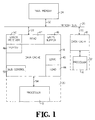
- the processing system 10 generally includes a first processor 12, a first data cache 14 associated with processor 12 and embodying the present invention, a second processor 16 and a second data cache 18 associated with the second processor 16.
- the first processor 12 and the first data cache 14 are preferably integrated together within a common integrated circuit 20.
- the second processor 16 and its associated second data cache 18 are preferably integrated together within a common integrated circuit.
- the processing system 10 further includes a main memory 24 which is integrated within a separate integrated circuit and thus is external to the first and second processor and data caches, and a memory bus 26.
- the first processor 12 and first data cache 14 are coupled to the memory bus 26 by a bi-directional bus 28.
- the second processor 16 and second data cache 18 are coupled to the memory bus 26 by another bidirectional bus 30.
- the main memory 24 is coupled to the memory bus 26 by a still further bi-directional bus 32.
- the first and second data caches 14 and 18 are utilized for storing data locally with respect to their associated first and second processors 12 and 16 respectively.
- a processor When a processor requires a block of data, it issues a load instruction for requesting the required block of data.
- the load instruction is first received by the data cache associated with the requesting processor for providing the requested block of data to the requesting processor locally in the event that the associated data cache contains the requested block of data.
- This configuration reduces the number of transactions which must occur on the memory bus 26 and maintains high processing performance because the provision of data locally to a requesting processor requires less time than obtaining the data from the external memory 24 over the memory bus 26.
- a data cache associated with a requesting processor If a data cache associated with a requesting processor is unable to provide the requesting processor with the requested data, it will then place the entire load instruction onto the memory bus 26 for fetching the requested data from the memory bus which is provided by either another data cache or the external memory 24.
- the data caches 14 and 18 are preferably arranged to perform a bus-watching function for load instructions from other processors. If a data cache sees a load instruction on the memory bus and is able to provide the requested data, it will intervene and provide the requested data before the external memory 24 is accessed. If none of the other caches in the processing system is able to provide the requested data, the external memory 24 then is accessed by the load instruction and provides the requested data to the requesting processor through its associated data cache.
- the data cache associated with the requesting processor receives the data from the external memory and stores the data locally and provides the data to its associated processor. In this manner, the requested data is now stored locally with respect to the requesting processor within its associated data cache so that when the block of data is once again required by the processor, it will be able to obtain the data locally from its associated data cache without requiring a memory access on the external bus 26.
- the data cache 18 is preferably identical to data cache 14 and, as a result, only data cache 14 will be described in detail. It should therefore be understood that the description of data cache 14 applies equally to data cache 18.
- Data cache 14 generally includes a logic section 40 which functions to implement the operation of data cache 14 in accordance with the flow diagram to be described hereinafter with respect to Figure 2, a read section 42, a load section 44, a memory section 46, a write buffer 48, an error receiver 50, and a bus control 52.
- the data cache 14 is coupled to its associated processor 12 over a bi-directional bus 54.
- the memory section 46 forms an internal storage means of the data cache 14 which includes a plurality of addressable storage locations.
- Each of the caches preferably includes such a memory and the main memory 24 also includes a plurality of addressable storage locations.
- Each of the storage locations is arranged to store a block of data which comprises four 8-bit bytes of data.
- Each block contains a group of lower order bits which contain the data and a group of higher order bits which contain a data tag.
- a processor requests a block of data, it provides a load instruction which includes a group of lower order bits containing the address of the storage location being accessed and a group of higher order bits which contain a data identifier.
- the data identifier is utilized by a data cache to determine if the data stored in the addressed storage location is the data requested by the requesting processor. To perform this function, the data cache receiving the instruction compares the data tag stored in the addressed storage location to the data identifier within the load instruction. If the data tag and the load instruction data identifier match, this indicates that the cache is able to provide the requested data. If the data tag and the load instruction data identifier do not match, this indicates that the cache is unable to provide the requested data.
- each storage location Also stored within each storage location is a validity bit and a modified bit.
- the validity bit indicates that the data stored in the particular storage location is valid data.
- the modified bit indicates if the data stored in the particular storage location is modified data.
- Each of the data caches in the processing system is arranged to maintain data consistency. In maintaining data consistency, some of the caches will be storing the same data. However, only the data cache most recently modifying the commonly stored data will have set the modified bit and thus will be considered the owner of the modified data. Each cache has the responsibility of preserving its valid and modified data within the processing system to prevent the valid and modified data from being deleted.
- the read section 42 fetches the requested data from the memory bus 26 in the event that the cache 14 does not contain the data requested by the processor 12 within its memory 46. If the memory 46 does not contain the data requested by the processor 12, the read section 42 places the entire load instruction onto the memory bus 26 for fetching the requested data from another data cache of the processing system or from the external memory 24. The read section 42, upon receiving the requested data from the memory bus 26, conveys the requested data to the memory 46 for storing the requested data in the storage location addressed by the load instruction. Also, during the same cycle, the load section 44 conveys the requested data to the processor 12.
- the write buffer 48 is arranged to temporarily store data which is to be written-back to the external memory 24. Such writing back of data to the external memory 24 is required when the data presently stored in a storage location addressed by the processor 12 is modified and valid data and data which is other than the data requested by the processor 12.
- the data presently stored in the addressed storage location is transferred to the write buffer 48 before the new data fetched from the memory bus 26 is written into the storage location addressed by the processor 12. This enables the data cache 14 to preserve the valid and modified data which would otherwise be deleted when the new and requested data is written into the storage location addressed by the processor 12 within the memory 46.
- the write buffer 48 then writes-back the valid and modified data to the external memory 24.
- the bus control 52 under control of the logic section 40 acquires the memory bus 26 prior to the fetching of the requested data by the read section 42 from the memory bus 26 and holds the memory bus 26 until the valid and modified data is written-back into the main memory 24 from the write buffer 48. This precludes another data cache from acquiring the memory bus before the foregoing operation is completed. If the bus control 52 did not hold the memory bus 26 until after the valid and modified data is written-back into the main memory 24, another data cache'may acquire the memory bus with a load instruction from its associated processor requiring the data cache 14 to be configured with the necessary hardware for comparing the load instruction address to the storage location addresses of both the memory 46 and the write buffer 48. Such extra hardware is not required because access to the memory bus 26 cannot be obtained by another cache until the cache writing-back data into external memory has completed the write-back procedure.
- the error receiver 50 of the data cache 14 is arranged to receive error messages from the memory bus 26 if an error is encountered during the write-back of data into external memory. Such an error message may arise, for example, where for some reason, the external memory 24 is unable to receive the valid and modified data being written-back to it.
- the valid and modified data is not permitted to remain in the write buffer. Instead, the valid and modified data within the write buffer 48 is transferred back to the memory 46 and is stored in the storage location addressed by the processor 12 in its load instruction.
- the valid and modified data originally stored in the addressed storage location is returned to the memory 46 within the addressed storage location and is thus written over the data requested by the processor 12 and newly acquired from the memory bus 26.
- the data cache 14 will be left in a state that appears as if the copy-back had been attempted before the loading of the new block of data into the processor 12.
- the bus control 52 continues to hold the bus 26 until the valid and modified data within the write buffer 48 is conveyed back to the storage location of memory 46 originally addressed by the processor 12. This further insures that bus-watching does not occur when the write buffer 48 contains the valid and modified data so that the aforementioned additional hardware is not needed.
- FIG. 2 it illustrates a flow diagram of the steps performed within the data cache 14 under control of the logic section 40 in response to receiving a load instruction from the processor 12.
- the logic section 40 begins in step 60 by receiving a load instruction or request from the processor 12.
- the logic section determines if the data requested by the processor 12 is presently stored in the storage location of memory 46 addressed by the processor 12 in its load instruction. In performing this step, as previously described, the logic section 40 compares the data tag stored in the addressed storage location to the data identifier within the load instruction.
- step 64 the logic section 40 then proceeds to step 64 to cause the requested data to be sent to the processor 12 from the memory 46 through the load section 44. The logic section then returns to start.
- step 62 If it is determined in step 62 that the data requested by the processor 12 is not presently stored in the storage location of memory 46 addressed by the processor 12 in its load instruction, as indicated by the data tag not matching the data identifier in the load instruction, the logic section 40 then proceeds to step 66 to determine if the data presently stored within the addressed storage location of memory 46 is valid and modified. In performing this step, the logic section 40 determines if the validity bit and the modified bit stored at the addressed storage location have been set.
- the logic section 40 causes the bus control 52 to first acquire the memory bus 26 and then causes the read section 42 to place the load instruction of the processor 12 onto the memory bus 26. In response to the load instruction placed on the memory bus 26, the read section 42 will receive the requested data from either another data cache which intervenes, such as data cache 18, or the external memory 24.
- the logic section 40 then proceeds to step 70 to cause the read section 42 to convey the requested data to the memory 46 for storage in the storage location addressed by the processor 12 in its load instruction, and to cause the load section 44 to convey the new and requested data to the processor 12.
- the logic section 40 then in step 72 causes the bus control 52 to release the memory bus 26 and then returns to start.
- step 66 the logic section 40 determines that the data presently stored in the memory 46 at the storage location addressed by the processor 12 in its load instruction is valid and modified, it will then, in accordance with the present invention, proceed to step 74 to cause the modified and valid data presently stored in the memory 46 at the addressed storage location to be conveyed to the write buffer 48.
- the valid and modified data stored in the memory 46 at the addressed storage location is not only valid and modified, but in addition, is data other than the data requested by the processor 12.
- the logic section 40 then proceeds to step 76 to cause the read section 42 to fetch the requested data from the memory bus.
- the logic section 40 first causes the bus control 52 to acquire the memory bus before placing the load instruction of the processor 12 onto the memory bus 26.
- step 78 Upon receipt of the requested data from either another cache or the external memory 24, the logic section then in step 78 causes the new data to be written into the memory 46 of data cache 14 within the storage location addressed by the processor 12. The logic section 40 also in step 78 causes the new and requested data to be loaded into the processor 12.
- step 80 causes the write buffer 48 to convey the valid and modified data stored therein back to the external memory 24. This step is taken after the new data is loaded into the processor 12 to permit the processor to continue with its executions. This improves processing performance because the processor 12 is permitted to continue processing while the valid and modified data within the write buffer 48 is written-back into the main memory 24.
- the logic section 40 causes the error receiver 50 to continue to detect for error messages associated with the write-back of the data in step 82. If the conveyance of the data is performed without error, the logic section then returns to start after causing the bus control 52 to release the memory bus 26 in step 86.
- the logic section then proceeds to step 84 wherein it causes the write buffer 48 to convey the valid and modified data stored therein to the memory 46 for storage within the storage location originally addressed by the processor 12 in its load instruction. Once the valid and modified data is transferred back from the write buffer to the memory 46, the logic section 40 causes the bus control 52 to release the bus and then returns to start.
- the present invention provides a system and method for handling errors occurring during the copy-back of data which not only precludes the data from being deleted, but in addition, negates the need for extra hardware for comparing load instructions to memory contents of both the memory of the data cache and the write buffer of the data cache. In accordance with the present invention, such extra hardware is not required for providing such comparisons with respect to the write buffer 48.
Landscapes
- Engineering & Computer Science (AREA)
- Theoretical Computer Science (AREA)
- Physics & Mathematics (AREA)
- General Engineering & Computer Science (AREA)
- General Physics & Mathematics (AREA)
- Quality & Reliability (AREA)
- Memory System Of A Hierarchy Structure (AREA)
- Techniques For Improving Reliability Of Storages (AREA)
Claims (4)
- Daten-Cache-Speicher (14,18) für ein Verarbeitungssystem (10), bei dem ein Speicher-Bus (26) einen externen Speicher (24) mit einem Prozessor (12,16) verbindet, wobei der Daten-Cache-Speicher mit dem Prozessor in eine IC-Schaltung (20,22) integriert ist und aufweist:eine Speichereinrichtung (46) mit mehreren adressierbaren Speicherstellen;einen Schreib-Puffer (48) zum vorübergehenden Speichern von Daten; undeine Logikeinrichtung (40), die mit dem Prozessor (12) verbunden ist und auf eine von dem Prozessor erzeugte Lade-Anforderung reagiert, wobei die Lade-Anforderung von dem Prozessor verlangte angeforderte Daten identifiziert und eine Speicherstellen-Adresse enthält, die eine der mehreren Speicherstellen bezeichnet, und wobei die bezeichnete Stelle die momentan gespeicherten Daten enthält und die Logikeinrichtung (40) feststellt, ob die momentan gespeicherten Daten die angeforderten Daten sind,dadurch gekennzeichnet, daß die Logikeinrichtung (40) die momentan gespeicherten Daten zu dem Schreib-Puffer (48) überträgt, wenn die momentan gespeicherten Daten gültig und modifiziert sind und es sich bei ihnen nicht um die angeforderten Daten handelt; die angeforderten Daten dann aus dem Speicher-Bus (26) abgerufen werden und an der bezeichneten Speicherstelle der Speichereinrichtung (46) gespeichert werden, und die Logikeinrichtung (40) ferner derart ausgebildet ist, daß sie die übertragenen Daten aus dem Schreib-Puffer (48) an den externen Speicher (24) ausgibt und auf ein Fehlersignal, das eine unzureichende Übermittlung der übertragenen Daten an den externen Speicher (24) angibt, reagiert, indem sie die übertragenen Daten zurück in die bezeichnete Speicherstelle der Speichereinrichtung (46) schreibt.
- Daten-Cache-Speicher nach Anspruch 1, ferner mit einer Bussteuereinrichtung (52) zum Anfordern des Speicher-Busses (26) zwecks Ermöglichung des Abrufens der angeforderten Daten, wobei die Bussteuereinrichtung derart ausgebildet ist, daß sie den Speicherbus belegt hält, bis die gültigen und modifizierten Daten zurück in die bezeichnete Speicherstelle geschrieben worden sind.
- Verfahren zum Betreiben eines Daten-Cache-Speichers (14, 18) in einem Verarbeitungssystem (10), bei dem ein Speicher-Bus (26) einen externen Speicher (24) mit einem Prozessor (12,16) verbindet, wobei der Daten-Cache-Speicher mit dem Prozessor in eine IC-Schaltung (20,22) integriert ist und das Verfahren die folgenden Schritte umfaßt:gekennzeichnet durchseitens des Daten-Cache-Speichers (14), Empfangen einer Prozessor-Lade-Anforderung, die eine Speicherstellen-Adresse für angeforderte Daten enthält; undFeststellen, ob die angeforderten Daten an der Adress-Speicherstelle der Speichereinrichtung (46) gespeichert sind,Übertragen der momentan an der Adress-Speicherstelle gespeicherten Daten zu einem Schreib-Puffer (48), wenn die momentan gespeicherten Daten gültig und modifiziert sind und es sich bei ihnen nicht um die angeforderten Daten handelt;Abrufen der angeforderten Daten aus dem Speicher-Bus (26), wenn die angeforderten Daten nicht an der Adress-Speicherstelle gespeichert sind;Speichern der angeforderten Daten an der Adress-Speicherstelle;Übertragen der angeforderten Daten an den Prozessor (12);Rückkopieren der gültigen und modifizierten Daten aus dem Schreib-Puffer (48) in den externen Speicher (24) über den Speicher-Bus; undauf dem Empfang eines Fehlersignals hin, das ein unzureichendes Rückkopieren der gültigen Daten aus dem Schreib-Puffer (48) in den externen Speicher (24) angibt, Übertragen der gültigen und modifizierten Daten zurück zu der Adress-Speicherstelle der Speichereinrichtung (46).
- Verfahren nach Anspruch 3, ferner mit den Schritten des Anforderns des Speicher-Busses (26) vor dem Abrufen der angeforderten Daten, und des Belegthaltens des Speicher-Busses, bis die gültigen und modifizierten Daten zurück in die adressierte Speicherstelle geschrieben worden sind.
Applications Claiming Priority (2)
| Application Number | Priority Date | Filing Date | Title |
|---|---|---|---|
| US07/650,681 US5295259A (en) | 1991-02-05 | 1991-02-05 | Data cache and method for handling memory errors during copy-back |
| US650681 | 1991-02-05 |
Publications (3)
| Publication Number | Publication Date |
|---|---|
| EP0498520A2 EP0498520A2 (de) | 1992-08-12 |
| EP0498520A3 EP0498520A3 (en) | 1993-07-14 |
| EP0498520B1 true EP0498520B1 (de) | 1998-10-14 |
Family
ID=24609860
Family Applications (1)
| Application Number | Title | Priority Date | Filing Date |
|---|---|---|---|
| EP92300017A Expired - Lifetime EP0498520B1 (de) | 1991-02-05 | 1992-01-02 | Datencache-Speicher und Verfahren zur Speicherfehlerbehandlung während Zurückschreiben |
Country Status (6)
| Country | Link |
|---|---|
| US (1) | US5295259A (de) |
| EP (1) | EP0498520B1 (de) |
| JP (1) | JPH04336641A (de) |
| AT (1) | ATE172310T1 (de) |
| DE (1) | DE69227267T2 (de) |
| ES (1) | ES2121818T3 (de) |
Families Citing this family (10)
| Publication number | Priority date | Publication date | Assignee | Title |
|---|---|---|---|---|
| US5761451A (en) * | 1992-11-04 | 1998-06-02 | Siemens Aktiengesellschaft | Configuration with several active and passive bus users |
| US5479636A (en) * | 1992-11-16 | 1995-12-26 | Intel Corporation | Concurrent cache line replacement method and apparatus in microprocessor system with write-back cache memory |
| US5594863A (en) * | 1995-06-26 | 1997-01-14 | Novell, Inc. | Method and apparatus for network file recovery |
| TW379298B (en) * | 1996-09-30 | 2000-01-11 | Toshiba Corp | Memory updating history saving device and memory updating history saving method |
| JP3489967B2 (ja) | 1997-06-06 | 2004-01-26 | 松下電器産業株式会社 | 半導体記憶装置及びキャッシュメモリ装置 |
| US20050240806A1 (en) * | 2004-03-30 | 2005-10-27 | Hewlett-Packard Development Company, L.P. | Diagnostic memory dump method in a redundant processor |
| US7441081B2 (en) * | 2004-12-29 | 2008-10-21 | Lsi Corporation | Write-back caching for disk drives |
| EP2073553A1 (de) * | 2007-12-21 | 2009-06-24 | Thomson Licensing | Verfahren und Vorrichtung zur Entblockungsfilterung eines Videobildes |
| US20130166251A1 (en) * | 2011-12-23 | 2013-06-27 | Robert A. Latimer | Particle monitoring with secure data logging |
| JP5800058B2 (ja) * | 2014-05-26 | 2015-10-28 | 富士通株式会社 | 情報処理装置、制御方法および制御プログラム |
Family Cites Families (9)
| Publication number | Priority date | Publication date | Assignee | Title |
|---|---|---|---|---|
| US4392200A (en) * | 1980-01-28 | 1983-07-05 | Digital Equipment Corporation | Cached multiprocessor system with pipeline timing |
| US4523275A (en) * | 1980-11-14 | 1985-06-11 | Sperry Corporation | Cache/disk subsystem with floating entry |
| US4933835A (en) * | 1985-02-22 | 1990-06-12 | Intergraph Corporation | Apparatus for maintaining consistency of a cache memory with a primary memory |
| US5025366A (en) * | 1988-01-20 | 1991-06-18 | Advanced Micro Devices, Inc. | Organization of an integrated cache unit for flexible usage in cache system design |
| US5065354A (en) * | 1988-09-16 | 1991-11-12 | Compaq Computer Corporation | Queued posted-write disk write method with improved error handling |
| US4995041A (en) * | 1989-02-03 | 1991-02-19 | Digital Equipment Corporation | Write back buffer with error correcting capabilities |
| DE3912705C2 (de) * | 1989-04-18 | 1996-06-20 | Siemens Nixdorf Inf Syst | Verfahren und Anordnung zur Steuerung des Datenaustausches bei Schreibanforderungen von Verarbeitungseinheiten an einen Cachespeicher |
| US5155824A (en) * | 1989-05-15 | 1992-10-13 | Motorola, Inc. | System for transferring selected data words between main memory and cache with multiple data words and multiple dirty bits for each address |
| US5197144A (en) * | 1990-02-26 | 1993-03-23 | Motorola, Inc. | Data processor for reloading deferred pushes in a copy-back data cache |
-
1991
- 1991-02-05 US US07/650,681 patent/US5295259A/en not_active Expired - Lifetime
-
1992
- 1992-01-02 AT AT92300017T patent/ATE172310T1/de not_active IP Right Cessation
- 1992-01-02 DE DE69227267T patent/DE69227267T2/de not_active Expired - Fee Related
- 1992-01-02 ES ES92300017T patent/ES2121818T3/es not_active Expired - Lifetime
- 1992-01-02 EP EP92300017A patent/EP0498520B1/de not_active Expired - Lifetime
- 1992-02-04 JP JP4017959A patent/JPH04336641A/ja not_active Withdrawn
Non-Patent Citations (1)
| Title |
|---|
| CHUANG ET AL. 'An On-Chip 72K Pseudo Two-Port Cache Memory Subsystem' * |
Also Published As
| Publication number | Publication date |
|---|---|
| DE69227267T2 (de) | 1999-06-10 |
| JPH04336641A (ja) | 1992-11-24 |
| US5295259A (en) | 1994-03-15 |
| ATE172310T1 (de) | 1998-10-15 |
| EP0498520A3 (en) | 1993-07-14 |
| EP0498520A2 (de) | 1992-08-12 |
| ES2121818T3 (es) | 1998-12-16 |
| DE69227267D1 (de) | 1998-11-19 |
Similar Documents
| Publication | Publication Date | Title |
|---|---|---|
| US5652859A (en) | Method and apparatus for handling snoops in multiprocessor caches having internal buffer queues | |
| US5740400A (en) | Reducing cache snooping overhead in a multilevel cache system with multiple bus masters and a shared level two cache by using an inclusion field | |
| EP0434250B1 (de) | Einrichtung und Verfahren zum Vermindern von Störungen in zweistufigen Cache-Speichern | |
| US5146603A (en) | Copy-back cache system having a plurality of context tags and setting all the context tags to a predetermined value for flushing operation thereof | |
| CA1278101C (en) | Paged virtual cache system | |
| KR100204741B1 (ko) | 제1및 제2캐시 메모리 사용방법 | |
| US4471429A (en) | Apparatus for cache clearing | |
| EP0118828A2 (de) | Befehlsabrufanordnung und -verfahren | |
| JP2002163148A (ja) | キャッシュメモリー付マルチ処理システム | |
| US5226146A (en) | Duplicate tag store purge queue | |
| US5850534A (en) | Method and apparatus for reducing cache snooping overhead in a multilevel cache system | |
| US6065099A (en) | System and method for updating the data stored in a cache memory attached to an input/output system | |
| US4831622A (en) | Apparatus for forcing a reload from main memory upon cache memory error | |
| US5263144A (en) | Method and apparatus for sharing data between processors in a computer system | |
| EP0498520B1 (de) | Datencache-Speicher und Verfahren zur Speicherfehlerbehandlung während Zurückschreiben | |
| US5479629A (en) | Method and apparatus for translation request buffer and requestor table for minimizing the number of accesses to the same address | |
| JPH0532775B2 (de) | ||
| US4648033A (en) | Look-aside buffer LRU marker controller | |
| US5636365A (en) | Hierarchical buffer memories for selectively controlling data coherence including coherence control request means | |
| EP0380861B1 (de) | Datenübereinstimmung zwischen Cache-Speichern und dem Hauptspeicher in einem Multiprozessorsystem | |
| US6078971A (en) | Input/output buffer and method for invalidating transferred data in direct memory access transfer | |
| EP0128353A2 (de) | Fehlerbehandlung für einen nichtdurchschreibbaren Cachespeicher | |
| JP3555847B2 (ja) | キャッシュメモリの障害処理装置、キャッシュメモリの障害処理方法、マルチプロセッサシステム | |
| KR100201671B1 (ko) | 컴퓨팅 시스템 및 컴퓨팅 시스템의 캐시 메모리 이용방법 | |
| EP0198574A2 (de) | Vorrichtung und Verfahren zur Datenkopienübereinstimmung in einer Mehrcachespeicherdatenverarbeitungsanordnung |
Legal Events
| Date | Code | Title | Description |
|---|---|---|---|
| PUAI | Public reference made under article 153(3) epc to a published international application that has entered the european phase |
Free format text: ORIGINAL CODE: 0009012 |
|
| AK | Designated contracting states |
Kind code of ref document: A2 Designated state(s): AT BE CH DE DK ES FR GB GR IT LI LU NL PT SE |
|
| PUAL | Search report despatched |
Free format text: ORIGINAL CODE: 0009013 |
|
| AK | Designated contracting states |
Kind code of ref document: A3 Designated state(s): AT BE CH DE DK ES FR GB GR IT LI LU NL PT SE |
|
| 17P | Request for examination filed |
Effective date: 19931220 |
|
| 17Q | First examination report despatched |
Effective date: 19970213 |
|
| GRAG | Despatch of communication of intention to grant |
Free format text: ORIGINAL CODE: EPIDOS AGRA |
|
| GRAG | Despatch of communication of intention to grant |
Free format text: ORIGINAL CODE: EPIDOS AGRA |
|
| GRAH | Despatch of communication of intention to grant a patent |
Free format text: ORIGINAL CODE: EPIDOS IGRA |
|
| GRAH | Despatch of communication of intention to grant a patent |
Free format text: ORIGINAL CODE: EPIDOS IGRA |
|
| GRAA | (expected) grant |
Free format text: ORIGINAL CODE: 0009210 |
|
| AK | Designated contracting states |
Kind code of ref document: B1 Designated state(s): AT BE CH DE DK ES FR GB GR IT LI LU NL PT SE |
|
| PG25 | Lapsed in a contracting state [announced via postgrant information from national office to epo] |
Ref country code: NL Free format text: LAPSE BECAUSE OF FAILURE TO SUBMIT A TRANSLATION OF THE DESCRIPTION OR TO PAY THE FEE WITHIN THE PRESCRIBED TIME-LIMIT Effective date: 19981014 Ref country code: LI Free format text: LAPSE BECAUSE OF FAILURE TO SUBMIT A TRANSLATION OF THE DESCRIPTION OR TO PAY THE FEE WITHIN THE PRESCRIBED TIME-LIMIT Effective date: 19981014 Ref country code: GR Free format text: LAPSE BECAUSE OF NON-PAYMENT OF DUE FEES Effective date: 19981014 Ref country code: FR Free format text: LAPSE BECAUSE OF FAILURE TO SUBMIT A TRANSLATION OF THE DESCRIPTION OR TO PAY THE FEE WITHIN THE PRESCRIBED TIME-LIMIT Effective date: 19981014 Ref country code: CH Free format text: LAPSE BECAUSE OF FAILURE TO SUBMIT A TRANSLATION OF THE DESCRIPTION OR TO PAY THE FEE WITHIN THE PRESCRIBED TIME-LIMIT Effective date: 19981014 Ref country code: BE Free format text: LAPSE BECAUSE OF FAILURE TO SUBMIT A TRANSLATION OF THE DESCRIPTION OR TO PAY THE FEE WITHIN THE PRESCRIBED TIME-LIMIT Effective date: 19981014 Ref country code: AT Free format text: LAPSE BECAUSE OF FAILURE TO SUBMIT A TRANSLATION OF THE DESCRIPTION OR TO PAY THE FEE WITHIN THE PRESCRIBED TIME-LIMIT Effective date: 19981014 |
|
| REF | Corresponds to: |
Ref document number: 172310 Country of ref document: AT Date of ref document: 19981015 Kind code of ref document: T |
|
| REG | Reference to a national code |
Ref country code: CH Ref legal event code: EP |
|
| REF | Corresponds to: |
Ref document number: 69227267 Country of ref document: DE Date of ref document: 19981119 |
|
| REG | Reference to a national code |
Ref country code: ES Ref legal event code: FG2A Ref document number: 2121818 Country of ref document: ES Kind code of ref document: T3 |
|
| PG25 | Lapsed in a contracting state [announced via postgrant information from national office to epo] |
Ref country code: LU Free format text: LAPSE BECAUSE OF NON-PAYMENT OF DUE FEES Effective date: 19990102 |
|
| PG25 | Lapsed in a contracting state [announced via postgrant information from national office to epo] |
Ref country code: SE Free format text: LAPSE BECAUSE OF FAILURE TO SUBMIT A TRANSLATION OF THE DESCRIPTION OR TO PAY THE FEE WITHIN THE PRESCRIBED TIME-LIMIT Effective date: 19990114 Ref country code: PT Free format text: LAPSE BECAUSE OF FAILURE TO SUBMIT A TRANSLATION OF THE DESCRIPTION OR TO PAY THE FEE WITHIN THE PRESCRIBED TIME-LIMIT Effective date: 19990114 Ref country code: DK Free format text: LAPSE BECAUSE OF FAILURE TO SUBMIT A TRANSLATION OF THE DESCRIPTION OR TO PAY THE FEE WITHIN THE PRESCRIBED TIME-LIMIT Effective date: 19990114 |
|
| PGFP | Annual fee paid to national office [announced via postgrant information from national office to epo] |
Ref country code: ES Payment date: 19990122 Year of fee payment: 8 |
|
| NLV1 | Nl: lapsed or annulled due to failure to fulfill the requirements of art. 29p and 29m of the patents act | ||
| EN | Fr: translation not filed | ||
| REG | Reference to a national code |
Ref country code: CH Ref legal event code: PL |
|
| PLBE | No opposition filed within time limit |
Free format text: ORIGINAL CODE: 0009261 |
|
| STAA | Information on the status of an ep patent application or granted ep patent |
Free format text: STATUS: NO OPPOSITION FILED WITHIN TIME LIMIT |
|
| 26N | No opposition filed | ||
| PG25 | Lapsed in a contracting state [announced via postgrant information from national office to epo] |
Ref country code: ES Free format text: LAPSE BECAUSE OF NON-PAYMENT OF DUE FEES Effective date: 20000103 |
|
| REG | Reference to a national code |
Ref country code: ES Ref legal event code: FD2A Effective date: 20011010 |
|
| PGFP | Annual fee paid to national office [announced via postgrant information from national office to epo] |
Ref country code: GB Payment date: 20011214 Year of fee payment: 11 |
|
| REG | Reference to a national code |
Ref country code: GB Ref legal event code: IF02 |
|
| PGFP | Annual fee paid to national office [announced via postgrant information from national office to epo] |
Ref country code: DE Payment date: 20020131 Year of fee payment: 11 |
|
| PG25 | Lapsed in a contracting state [announced via postgrant information from national office to epo] |
Ref country code: GB Free format text: LAPSE BECAUSE OF NON-PAYMENT OF DUE FEES Effective date: 20030102 |
|
| PG25 | Lapsed in a contracting state [announced via postgrant information from national office to epo] |
Ref country code: DE Free format text: LAPSE BECAUSE OF NON-PAYMENT OF DUE FEES Effective date: 20030801 |
|
| GBPC | Gb: european patent ceased through non-payment of renewal fee |
Effective date: 20030102 |
|
| PG25 | Lapsed in a contracting state [announced via postgrant information from national office to epo] |
Ref country code: IT Free format text: LAPSE BECAUSE OF NON-PAYMENT OF DUE FEES Effective date: 20050102 |