EP0498400A1 - Thermal head - Google Patents
Thermal head Download PDFInfo
- Publication number
- EP0498400A1 EP0498400A1 EP92101914A EP92101914A EP0498400A1 EP 0498400 A1 EP0498400 A1 EP 0498400A1 EP 92101914 A EP92101914 A EP 92101914A EP 92101914 A EP92101914 A EP 92101914A EP 0498400 A1 EP0498400 A1 EP 0498400A1
- Authority
- EP
- European Patent Office
- Prior art keywords
- conductive
- thermal head
- package
- electrostatically
- resinous
- Prior art date
- Legal status (The legal status is an assumption and is not a legal conclusion. Google has not performed a legal analysis and makes no representation as to the accuracy of the status listed.)
- Granted
Links
Images


Classifications
-
- B—PERFORMING OPERATIONS; TRANSPORTING
- B41—PRINTING; LINING MACHINES; TYPEWRITERS; STAMPS
- B41J—TYPEWRITERS; SELECTIVE PRINTING MECHANISMS, i.e. MECHANISMS PRINTING OTHERWISE THAN FROM A FORME; CORRECTION OF TYPOGRAPHICAL ERRORS
- B41J2/00—Typewriters or selective printing mechanisms characterised by the printing or marking process for which they are designed
- B41J2/315—Typewriters or selective printing mechanisms characterised by the printing or marking process for which they are designed characterised by selective application of heat to a heat sensitive printing or impression-transfer material
- B41J2/32—Typewriters or selective printing mechanisms characterised by the printing or marking process for which they are designed characterised by selective application of heat to a heat sensitive printing or impression-transfer material using thermal heads
- B41J2/335—Structure of thermal heads
- B41J2/33505—Constructional details
- B41J2/3353—Protective layers
-
- B—PERFORMING OPERATIONS; TRANSPORTING
- B41—PRINTING; LINING MACHINES; TYPEWRITERS; STAMPS
- B41J—TYPEWRITERS; SELECTIVE PRINTING MECHANISMS, i.e. MECHANISMS PRINTING OTHERWISE THAN FROM A FORME; CORRECTION OF TYPOGRAPHICAL ERRORS
- B41J2/00—Typewriters or selective printing mechanisms characterised by the printing or marking process for which they are designed
- B41J2/315—Typewriters or selective printing mechanisms characterised by the printing or marking process for which they are designed characterised by selective application of heat to a heat sensitive printing or impression-transfer material
- B41J2/32—Typewriters or selective printing mechanisms characterised by the printing or marking process for which they are designed characterised by selective application of heat to a heat sensitive printing or impression-transfer material using thermal heads
- B41J2/335—Structure of thermal heads
- B41J2/33555—Structure of thermal heads characterised by type
- B41J2/3357—Surface type resistors
-
- H—ELECTRICITY
- H05—ELECTRIC TECHNIQUES NOT OTHERWISE PROVIDED FOR
- H05F—STATIC ELECTRICITY; NATURALLY-OCCURRING ELECTRICITY
- H05F3/00—Carrying-off electrostatic charges
-
- H—ELECTRICITY
- H10—SEMICONDUCTOR DEVICES; ELECTRIC SOLID-STATE DEVICES NOT OTHERWISE PROVIDED FOR
- H10W—GENERIC PACKAGES, INTERCONNECTIONS, CONNECTORS OR OTHER CONSTRUCTIONAL DETAILS OF DEVICES COVERED BY CLASS H10
- H10W72/00—Interconnections or connectors in packages
- H10W72/851—Dispositions of multiple connectors or interconnections
- H10W72/874—On different surfaces
- H10W72/884—Die-attach connectors and bond wires
Definitions
- This invention relates generally to thermal heads which are widely used in facsimile machines, word processors and so forth. More specifically, the invention relates to a thermal head of the type which comprises a head circuit board carrying a heating resistor line divisionally actuated by at least one drive IC.
- a thermal head comprises an elongate head circuit board which carries a heating resistor line extending along one longitudinal edge of the circuit board.
- the circuit board also carries an array of drive IC's for divisionally actuating the resistor line to provide a line of multiple heating dots, and a printed conductor pattern which makes a sophisticated circuit arrangement on the circuit board.
- the Japanese utility model document also proposes that the metallic cover member is grounded.
- an ink ribbon and/or paper including thermosensitive paper
- the electrostatic charge of the ribbon and/or paper induces opposite electrostatic charge on the cover member. If this happens, the grounded cover member allows electrostatic charge to escape from the cover member, thereby preventing the drive IC's from being electrostatically disturbed or damaged.
- the thermal head disclosed in the above Japanese utility model document is disadvantageous in that the metallic cover member increases the size and weight of the thermal head.
- the use of the resinous package is defective in that it cannot eliminate the problem of electrostatic influences, as opposed to the metallic cover member disclosed in the Japanese utility model document.
- the package is made of epoxy resin, unsaturated polyester resin or polyetheramide resin
- the volume resistivity of the package is approximately from 1013 to 1014 ( ⁇ cm) or even higher. Due to such a high volume resistivity or high electrical insulation, the resinous package is easily charged electrostatically at a high voltage with a small electrostatic capacity. As a result, the drive IC's becomes liable to malfunction, and the heating resistor may be damaged by discharging upon passage of the oppositely charged ink ribbon or paper.
- an object of the present invention to provide a thermal head which, while being capable of realizing reduction in size and weight, prevents electrostatic disturbances and/or damages by effectively removing electrostatic charging.
- a thermal head comprising a head circuit board having a surface carrying a heating resistor means and at least one drive element for heating the resistor means, said at least one drive element being enclosed in a resinous package, characterized in that at least a surface portion of the resinous package is electrostatically conductive but electrically non-conductive to work as antistat.
- the thermal head mainly comprises a metallic support plate 1 (see Fig. 3) made for example of aluminum to serve also as a heat sink, an elongate head circuit board 2 made of an insulating material such as ceramic, and a flexible connector board 8 reinforced by a backing 3.
- the head circuit board 2 and the backing 3 are fixed to the support plate 1.
- the head circuit board 2 has a surface which carries a heating resistor line 4 extending along one longitudinal edge of the board.
- the surface of the head circuit board also carries an array of drive IC's 5 for divisionally actuating the resistor line 4, thereby providing a line of heating dots.
- the surface of the head circuit board further carries a printed conductor pattern which includes individual electrodes 6 (see Fig. 2) connected to the resistor line 4, a wiring conductor pattern 9, and other conductors (not shown).
- the individual electrodes 6 and the wiring conductor pattern 9 are connected to the respective drive IC's 5 through wires 7.
- selected spots or dots of the resistor line 4 are heated by supplying electric power through selected ones of the individual electrodes 6.
- the wiring conductor pattern 9 has a connection terminal portion 9a arranged centrally adjacent to a longitudinal edge of the head circuit board 2 which is located opposite to the resistor line 4.
- the flexible connector board 8 projects beyond the backing 3.
- the underside of the connector board 8 is formed with a printed conductor patter (not shown) in corresponding relation to the connection terminal portion 9a of the head circuit board 2, and the connector board is overlapped partially on the head circuit board 2 at the connection terminal portion 9a thereof.
- the backing 3 may be made for example of a glass-fiber-reinforced epoxy resin.
- the flexible connector board 8 together with the backing 3 is fixed to the support plate 1 by means of bolts 10 (only one shown in Fig. 3) screwed in the support plate 11 through a presser member 11, the connector board 8 and the backing 3. Further, the flexible connector board 8 is held in intimate contact with the head circuit board 2 by an elastic rod 12 arranged between the pressure member 11 and the connector board 8.
- the connector board 8 (namely, the unillustrated conductor pattern thereof) is electrically connected to the head circuit board 2 (namely, the wiring pattern 9).
- the underside of the backing 3 carries a connector (or connectors) 13 for connection to external circuitry through a flexible cable (not shown) for example.
- the array of drive IC's 5 is enclosed in an antistatic resinous package 14.
- the package 14 is entirely made of a synthetic resin which is electrostatically conductive but electrically non-conductive.
- the package 14 should additionally enclose the wires 7 connecting the respective drive IC's 5 to the individual electrodes 6 and the wiring pattern 9.
- the antistatic resinous package 14 may be formed for example by the following procedure. First, electrically non-conductive matrix resin (e.g. polyetheramide resin or epoxy resin) in paste form is mixed with electrically conductive substance (e.g. about 20 wt.% of carbon) and kneaded. Then, the mixture paste is applied to the head circuit board 2 to completely enclose the drive IC array 5 and the wires 7. Finally, the applied paste is allowed to harden.
- electrically non-conductive matrix resin e.g. polyetheramide resin or epoxy resin
- electrically conductive substance e.g. about 20 wt.% of carbon
- the resulting resinous package 14 When polyetheramide resin or epoxy resin is used as the matrix resin for mixture with about 20 wt.% of carbon as the conductive substance, the resulting resinous package 14 will have a volume resistivity of about 105 ( ⁇ cm). The volume resistivity will further decrease as the carbon content increases.
- the resinous package 14 is considered to be electrostatically conductive but electrically non-conductive when the volume resistivity thereof is within a range of 104-1010( ⁇ cm), preferably 105 - 109 ( ⁇ cm).
- the resinous package 14 formed as above can work effectively as antistat.
- examples of electrically conductive substance for mixture with the non-conductive matrix resin include silver powder, copper powder, various surfactants, and so forth.
- examples of applicable surfactants include anionic surfactants (such as alkyl sulfonate type, alkyl aryl sulfonate type, alkylamine sulfonate type), cationic surfactants (such as quaternary ammonium salt type, quaternary ammonium resin type, pyridinium salt type), non-ionic surfactants (such as ether type, amine or amide type, etanolamide type), and ampho-ionic surfactants (such as betaine type).
- anionic surfactants such as alkyl sulfonate type, alkyl aryl sulfonate type, alkylamine sulfonate type
- cationic surfactants such as quaternary ammonium salt type, quaternary ammonium resin type, pyridinium salt type
- a platen 15 (see Fig. 3) is disposed in opposition to the resistor line 4 of the head circuit board 2, and paper 17 and a thermosensitive ink ribbon 16 are passed between the platen 15 and the resistor line 4 in the direction of an arrow A in Fig. 3.
- the respective drive IC's 5 are actuated in response to externally supplied signals to heat selected spots or dots of the resistor line 4, thereby performing intended printing onto the paper 17.
- the ink ribbon 16 and/or the paper 17 generate static electricity due to friction relative to each other and/or the platen 15.
- the antistatic resinous package 14 which is electrostatically conductive, continuously allows the generated static electricity to escape along its surface. Thus, it is possible to effectively prevent the drive IC's 5 and the resistor line 4 from being electrostatically disturbed or damaged.
- Fig. 4 shows a thermal head according to a second embodiment of the present invention which differs from that of the first embodiment only in one point.
- the thermal head of Fig. 4 incorporates an antistatic resinous package 14A which consists of an inner portion 18 entirely enclosing the drive IC's 5 and the wires 7, and a surface portion or layer 19 covering the inner portion 18.
- the inner portion 18 is made for example of thermosetting epoxy resin which is highly non-conductive electrically (electrostatically non-conductive as well), whereas the antistatic surface layer 19 is made of a resinous material similar to that of the first embodiment to become electrostatically conductive but electrically non-conductive.
- the thickness of the surface layer 19 may be relatively small or relatively large.
- the antistatic resinous package 14A of Fig. 4 is capable of more reliably preventing the drive IC's 5 from electrostatic disturbances (noises and/or operation failures) and damages even if the surface layer 19 is electrostatically charged to a greater extent than normally expected. Obviously, the resistor line 4 is also prevented from electrostatic damages similarly to the first embodiment. It should be appreciated that electrostatic charging occurs only at the surface of the resinous package 14A, so that it suffices to provide an antistatic layer only at the surface of the package.
- Fig. 5 represents an antistatic resinous package 14B according to a third embodiment of the present invention.
- the package 14B of the second embodiment has a double structure which consists of an inner portion 20 entirely enclosing the drive IC's 5 and the wires 7, and a surface portion or layer 21 covering the inner portion 20.
- the inner portion 20 is made of relatively soft resin such as silicone resin which is electrostatically and electrically non-conductive
- the antistatic surface layer 21 is made of a resinous material similar to that of the first embodiment to become electrostatically conductive but electrically non-conductive.
- the thickness of the antistatic surface layer 21 is rendered sufficiently large to prevent the inner portion 20 from being mechanically deformed by external forces.
- the antistatic resinous package 14B of the third embodiment allows thermal expansion and contraction of the drive IC's 5.
- the drive IC's are prevented from mechanically damaged by such expansion and contraction.
- the antistatic surface layer 21 provides the same advantages as already described.
- an antistatic resinous package 14C has a triple structure. Specifically, the package 14C consists of an inner portion 22 entirely enclosing the drive IC's 5 and the wires 7, an intermediate portion or layer 23 enclosing the inner portion 22, and a surface portion or layer 24 covering the intermediate layer 23.
- the inner portion 22 is made of relatively soft resin such as silicone resin which is electrostatically and electrically non-conductive
- the intermediate layer 23 is made for example of thermosetting epoxy resin which is relatively hard and highly non-conductive electrically (electrostatically non-conductive as well).
- the antistatic surface layer 21 is made of a resinous material similar to that of the first embodiment to become electrostatically conductive but electrically non-conductive.
- the thermal expansion and contraction of the drive IC's 5 are allowed by the soft inner portion 22, while the mechanical strength against external forces is provided by the hard intermediate layer 23. Further, the antistatic surface layer 24 prevents adverse influences which might be caused by electrostatic charging, as already described. Thus, the antistatic resinous package 14C of this embodiment is advantageous in various respects.
- Fig. 7 shows a thermal head according to a fifth embodiment of the present invention which differs from the first embodiment only in that a flexible connector board 8 is electrically connected to the head circuit board 2 by soldering or by using an electrically conductive adhesive.
- a flexible connector board 8 is electrically connected to the head circuit board 2 by soldering or by using an electrically conductive adhesive.
Landscapes
- Electronic Switches (AREA)
- Elimination Of Static Electricity (AREA)
- Accessory Devices And Overall Control Thereof (AREA)
Abstract
Description
- This invention relates generally to thermal heads which are widely used in facsimile machines, word processors and so forth. More specifically, the invention relates to a thermal head of the type which comprises a head circuit board carrying a heating resistor line divisionally actuated by at least one drive IC.
- In general, a thermal head comprises an elongate head circuit board which carries a heating resistor line extending along one longitudinal edge of the circuit board. The circuit board also carries an array of drive IC's for divisionally actuating the resistor line to provide a line of multiple heating dots, and a printed conductor pattern which makes a sophisticated circuit arrangement on the circuit board.
- In such a thermal head, because the drive IC's are relatively sensitive to shocks and mechanical forces, it is proposed to protect the drive IC array by a metallic cover member, as disclosed for example in Japanese Utility Model Application Laid-open No. 57-121543 (Laid-open: July, 28, 1982). Obviously, the cover member prevents the drive IC array from coming into contact with any external objects.
- Further, the Japanese utility model document also proposes that the metallic cover member is grounded. During operation of the thermal head for printing, an ink ribbon and/or paper (including thermosensitive paper) may be electrostatically charged due to inevitable sliding movement thereof relative to the heating resistor and/or the platen, and the electrostatic charge of the ribbon and/or paper induces opposite electrostatic charge on the cover member. If this happens, the grounded cover member allows electrostatic charge to escape from the cover member, thereby preventing the drive IC's from being electrostatically disturbed or damaged.
- However, the thermal head disclosed in the above Japanese utility model document is disadvantageous in that the metallic cover member increases the size and weight of the thermal head.
- For realization of size and weight reduction, it has been recently proposed to enclose the array of drive IC's and their respective wires in a resinous package which is made of a relatively hard resin such as epoxy resin, unsaturated polyester resin or polyetheramide resin. The use of the resinous package makes it unnecessary to use any protective cover member.
- However, the use of the resinous package is defective in that it cannot eliminate the problem of electrostatic influences, as opposed to the metallic cover member disclosed in the Japanese utility model document. Specifically, when the package is made of epoxy resin, unsaturated polyester resin or polyetheramide resin, the volume resistivity of the package is approximately from 10¹³ to 10¹⁴ (Ω·cm) or even higher. Due to such a high volume resistivity or high electrical insulation, the resinous package is easily charged electrostatically at a high voltage with a small electrostatic capacity. As a result, the drive IC's becomes liable to malfunction, and the heating resistor may be damaged by discharging upon passage of the oppositely charged ink ribbon or paper.
- It is, therefore, an object of the present invention to provide a thermal head which, while being capable of realizing reduction in size and weight, prevents electrostatic disturbances and/or damages by effectively removing electrostatic charging.
- According to the present invention, there is provided a thermal head comprising a head circuit board having a surface carrying a heating resistor means and at least one drive element for heating the resistor means, said at least one drive element being enclosed in a resinous package, characterized in that at least a surface portion of the resinous package is electrostatically conductive but electrically non-conductive to work as antistat.
- The present invention will now be described further, by way of example only, with reference to the accompanying drawings, in which:
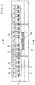
- Fig. 1 is a plan view schematically showing a thermal head according to a first embodiment of the present invention;
- Fig. 2 is an enlarged fragmentary plan view showing a circuit arrangement near a drive IC incorporated in the thermal head of Fig. 1;
- Fig. 3 is an enlarged sectional view taken along lines III-III in Fig. 1;
- Fig. 4 is a fragmentary transverse sectional view showing a thermal head according to a second embodiment of the present invention;
- Fig. 5 is a sectional view similar to Fig. 4 but showing a thermal head according to a third embodiment of the present invention;
- Fig. 6 is a sectional view also similar to Fig. 4 but showing a thermal head according to a fourth embodiment of the present invention; and
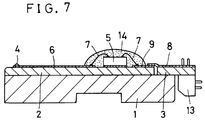
- Fig. 7 is a sectional view similar to Fig. 3 but showing a thermal head according to a fifth embodiment of the present invention.
- Referring first to Figs. 1 to 3 of the accompanying drawings, there is illustrated a thermal head according to a first embodiment of the present invention. The thermal head mainly comprises a metallic support plate 1 (see Fig. 3) made for example of aluminum to serve also as a heat sink, an elongate
head circuit board 2 made of an insulating material such as ceramic, and aflexible connector board 8 reinforced by abacking 3. Thehead circuit board 2 and the backing 3 (with the flexible connector board 8) are fixed to thesupport plate 1. - The
head circuit board 2 has a surface which carries aheating resistor line 4 extending along one longitudinal edge of the board. The surface of the head circuit board also carries an array of drive IC's 5 for divisionally actuating theresistor line 4, thereby providing a line of heating dots. The surface of the head circuit board further carries a printed conductor pattern which includes individual electrodes 6 (see Fig. 2) connected to theresistor line 4, awiring conductor pattern 9, and other conductors (not shown). - As shown in Figs. 2 and 3, the
individual electrodes 6 and thewiring conductor pattern 9 are connected to the respective drive IC's 5 throughwires 7. Thus, selected spots or dots of theresistor line 4 are heated by supplying electric power through selected ones of theindividual electrodes 6. Thewiring conductor pattern 9 has aconnection terminal portion 9a arranged centrally adjacent to a longitudinal edge of thehead circuit board 2 which is located opposite to theresistor line 4. - The flexible connector board 8 projects beyond the
backing 3. The underside of theconnector board 8 is formed with a printed conductor patter (not shown) in corresponding relation to theconnection terminal portion 9a of thehead circuit board 2, and the connector board is overlapped partially on thehead circuit board 2 at theconnection terminal portion 9a thereof. Thebacking 3 may be made for example of a glass-fiber-reinforced epoxy resin. - In assembly, the
flexible connector board 8 together with thebacking 3 is fixed to thesupport plate 1 by means of bolts 10 (only one shown in Fig. 3) screwed in thesupport plate 11 through apresser member 11, theconnector board 8 and thebacking 3. Further, theflexible connector board 8 is held in intimate contact with thehead circuit board 2 by anelastic rod 12 arranged between thepressure member 11 and theconnector board 8. Thus, the connector board 8 (namely, the unillustrated conductor pattern thereof) is electrically connected to the head circuit board 2 (namely, the wiring pattern 9). Further, the underside of thebacking 3 carries a connector (or connectors) 13 for connection to external circuitry through a flexible cable (not shown) for example. - According to the present invention, the array of drive IC's 5 is enclosed in an antistatic
resinous package 14. Specifically, according the embodiment of Figs. 1-3, thepackage 14 is entirely made of a synthetic resin which is electrostatically conductive but electrically non-conductive. Preferably, thepackage 14 should additionally enclose thewires 7 connecting the respective drive IC's 5 to theindividual electrodes 6 and thewiring pattern 9. - The antistatic
resinous package 14 may be formed for example by the following procedure. First, electrically non-conductive matrix resin (e.g. polyetheramide resin or epoxy resin) in paste form is mixed with electrically conductive substance (e.g. about 20 wt.% of carbon) and kneaded. Then, the mixture paste is applied to thehead circuit board 2 to completely enclose thedrive IC array 5 and thewires 7. Finally, the applied paste is allowed to harden. - When polyetheramide resin or epoxy resin is used as the matrix resin for mixture with about 20 wt.% of carbon as the conductive substance, the resulting
resinous package 14 will have a volume resistivity of about 10⁵ (Ω·cm). The volume resistivity will further decrease as the carbon content increases. - In general, the
resinous package 14 is considered to be electrostatically conductive but electrically non-conductive when the volume resistivity thereof is within a range of 10⁴-10¹⁰(Ω·cm), preferably 10⁵ - 10⁹ (Ω·cm). Thus, theresinous package 14 formed as above can work effectively as antistat. - In addition to carbon, examples of electrically conductive substance for mixture with the non-conductive matrix resin include silver powder, copper powder, various surfactants, and so forth. Examples of applicable surfactants include anionic surfactants (such as alkyl sulfonate type, alkyl aryl sulfonate type, alkylamine sulfonate type), cationic surfactants (such as quaternary ammonium salt type, quaternary ammonium resin type, pyridinium salt type), non-ionic surfactants (such as ether type, amine or amide type, etanolamide type), and ampho-ionic surfactants (such as betaine type).
- In operation, a platen 15 (see Fig. 3) is disposed in opposition to the
resistor line 4 of thehead circuit board 2, andpaper 17 and athermosensitive ink ribbon 16 are passed between theplaten 15 and theresistor line 4 in the direction of an arrow A in Fig. 3. The respective drive IC's 5 are actuated in response to externally supplied signals to heat selected spots or dots of theresistor line 4, thereby performing intended printing onto thepaper 17. - During the operation, the
ink ribbon 16 and/or thepaper 17 generate static electricity due to friction relative to each other and/or theplaten 15. However, the antistaticresinous package 14, which is electrostatically conductive, continuously allows the generated static electricity to escape along its surface. Thus, it is possible to effectively prevent the drive IC's 5 and theresistor line 4 from being electrostatically disturbed or damaged. - Fig. 4 shows a thermal head according to a second embodiment of the present invention which differs from that of the first embodiment only in one point.
- Specifically, the thermal head of Fig. 4 incorporates an
antistatic resinous package 14A which consists of aninner portion 18 entirely enclosing the drive IC's 5 and thewires 7, and a surface portion orlayer 19 covering theinner portion 18. Theinner portion 18 is made for example of thermosetting epoxy resin which is highly non-conductive electrically (electrostatically non-conductive as well), whereas theantistatic surface layer 19 is made of a resinous material similar to that of the first embodiment to become electrostatically conductive but electrically non-conductive. The thickness of thesurface layer 19 may be relatively small or relatively large. - Because of the high insulating ability of the
inner portion 18, theantistatic resinous package 14A of Fig. 4 is capable of more reliably preventing the drive IC's 5 from electrostatic disturbances (noises and/or operation failures) and damages even if thesurface layer 19 is electrostatically charged to a greater extent than normally expected. Obviously, theresistor line 4 is also prevented from electrostatic damages similarly to the first embodiment. It should be appreciated that electrostatic charging occurs only at the surface of theresinous package 14A, so that it suffices to provide an antistatic layer only at the surface of the package. - Fig. 5 represents an
antistatic resinous package 14B according to a third embodiment of the present invention. - Similarly to the first embodiment, the
package 14B of the second embodiment has a double structure which consists of aninner portion 20 entirely enclosing the drive IC's 5 and thewires 7, and a surface portion orlayer 21 covering theinner portion 20. Theinner portion 20 is made of relatively soft resin such as silicone resin which is electrostatically and electrically non-conductive, whereas theantistatic surface layer 21 is made of a resinous material similar to that of the first embodiment to become electrostatically conductive but electrically non-conductive. Preferably, the thickness of theantistatic surface layer 21 is rendered sufficiently large to prevent theinner portion 20 from being mechanically deformed by external forces. - Due to the soft nature of the
inner portion 20, theantistatic resinous package 14B of the third embodiment allows thermal expansion and contraction of the drive IC's 5. Thus, the drive IC's are prevented from mechanically damaged by such expansion and contraction. Obviously, theantistatic surface layer 21 provides the same advantages as already described. - According to a fourth embodiment shown in Fig. 6, an
antistatic resinous package 14C has a triple structure. Specifically, thepackage 14C consists of aninner portion 22 entirely enclosing the drive IC's 5 and thewires 7, an intermediate portion orlayer 23 enclosing theinner portion 22, and a surface portion orlayer 24 covering theintermediate layer 23. Theinner portion 22 is made of relatively soft resin such as silicone resin which is electrostatically and electrically non-conductive, whereas theintermediate layer 23 is made for example of thermosetting epoxy resin which is relatively hard and highly non-conductive electrically (electrostatically non-conductive as well). Further, theantistatic surface layer 21 is made of a resinous material similar to that of the first embodiment to become electrostatically conductive but electrically non-conductive. - Obviously, according to the fourth embodiment of Fig. 6, the thermal expansion and contraction of the drive IC's 5 are allowed by the soft
inner portion 22, while the mechanical strength against external forces is provided by the hardintermediate layer 23. Further, theantistatic surface layer 24 prevents adverse influences which might be caused by electrostatic charging, as already described. Thus, theantistatic resinous package 14C of this embodiment is advantageous in various respects. - Fig. 7 shows a thermal head according to a fifth embodiment of the present invention which differs from the first embodiment only in that a
flexible connector board 8 is electrically connected to thehead circuit board 2 by soldering or by using an electrically conductive adhesive. Thus, in this embodiment, no presser member and no mounting means therefor are required, thereby simplifying the overall arrangement of the thermal head. - The invention being thus described, it is obvious that the same may be varied in many ways. Such variations are not to be regarded as a departure from the spirit and scope of the invention, and all such modifications as would be obvious to those skilled in the art are intended to be included within the scope of the following claims.
Claims (7)
- A thermal head comprising a head circuit board (2) having a surface carrying a heating resistor means (4) and at least one drive element (5) for heating the resistor means, said at least one drive element being enclosed in a resinous package (14, 14A, 14B, 14C), characterized in that
at least a surface portion (19, 21, 24) of the resinous package (14, 14A, 14B, 14C) is electrostatically conductive but electrically non-conductive to work as antistat. - The thermal head according to claim 1, wherein the entirety of the resinous package (14) is electrostatically conductive but electrically non-conductive.
- The thermal head according to claim 1, wherein the resinous package (14A, 14B) has an inner portion (18, 20) which is electrostatically and electrically non-conductive, the surface portion (19, 21) of the resinous package alone being electrostatically conductive but electrically non-conductive.
- The thermal head according to claim 3, wherein the inner portion (18, 20) of the resinous package (14A, 14B) is made of resin which is highly non-conductive electrically.
- The thermal head according to claim 3, wherein the inner portion (20) of the resinous package (14B) is made of a relatively soft resin.
- The thermal head according to claim 1, wherein the resinous package (14C) has an inner portion (22) which is made of a relatively soft resin, the resinous package further having an intermediate portion (23) which is made of a relatively hard resin, the inner and intermediate portions being electrostatically and electrically non-conductive, the surface portion (24) of the resinous package alone being electrostatically conductive but electrically non-conductive.
- The thermal head according to claim 1, wherein at least the surface portion (19, 21, 24) of the resinous package (14, 14A, 14B, 14C) is made of matrix resin which contains a predetermined percentage of electrically conductive substance.
Applications Claiming Priority (2)
| Application Number | Priority Date | Filing Date | Title |
|---|---|---|---|
| JP3038046A JP3016884B2 (en) | 1991-02-06 | 1991-02-06 | Thermal head |
| JP38046/91 | 1991-02-06 |
Publications (2)
| Publication Number | Publication Date |
|---|---|
| EP0498400A1 true EP0498400A1 (en) | 1992-08-12 |
| EP0498400B1 EP0498400B1 (en) | 1996-01-24 |
Family
ID=12514590
Family Applications (1)
| Application Number | Title | Priority Date | Filing Date |
|---|---|---|---|
| EP92101914A Expired - Lifetime EP0498400B1 (en) | 1991-02-06 | 1992-02-05 | Thermal head |
Country Status (5)
| Country | Link |
|---|---|
| US (1) | US5278580A (en) |
| EP (1) | EP0498400B1 (en) |
| JP (1) | JP3016884B2 (en) |
| KR (1) | KR970004233B1 (en) |
| DE (1) | DE69207785T2 (en) |
Cited By (3)
| Publication number | Priority date | Publication date | Assignee | Title |
|---|---|---|---|---|
| EP0547596A3 (en) * | 1991-12-19 | 1993-08-18 | Canon Kabushiki Kaisha | Ink jet recording head, ink jet recording head cartridge and recording apparatus using same |
| DE19614914A1 (en) * | 1996-04-16 | 1997-10-23 | Telesensomatic Gmbh | Transponder arrangement with single- or multi-layer integrated circuit |
| EP0891868A3 (en) * | 1997-07-17 | 1999-07-28 | Fuji Photo Film Co., Ltd. | Thermal head |
Families Citing this family (13)
| Publication number | Priority date | Publication date | Assignee | Title |
|---|---|---|---|---|
| US5764267A (en) * | 1992-05-15 | 1998-06-09 | Fuji Xerox Co., Ltd. | Conduction recording head |
| JPH0732634A (en) * | 1993-07-22 | 1995-02-03 | Seiko Instr Inc | Printer |
| WO1997004965A1 (en) * | 1995-07-31 | 1997-02-13 | Rohm Co., Ltd. | Linear thermal print head and linear thermal print head apparatus |
| US5936581A (en) * | 1997-03-03 | 1999-08-10 | Motorola, Inc. | Radio frequency switch assembly |
| JP2001353893A (en) * | 2000-06-14 | 2001-12-25 | Kyocera Corp | Thermal head |
| JP2002011900A (en) * | 2000-06-29 | 2002-01-15 | Kyocera Corp | Thermal head |
| JP4398766B2 (en) * | 2004-03-30 | 2010-01-13 | アルプス電気株式会社 | Thermal head and manufacturing method thereof |
| CN102555515B (en) * | 2010-11-19 | 2015-08-26 | 罗姆股份有限公司 | Thermal printing head and manufacture method thereof |
| US8462187B2 (en) * | 2010-11-30 | 2013-06-11 | Rohm Co., Ltd. | Thermal print head |
| JP6178669B2 (en) * | 2012-08-29 | 2017-08-09 | ローム株式会社 | Thermal print head and thermal printer |
| WO2015029913A1 (en) * | 2013-08-26 | 2015-03-05 | 京セラ株式会社 | Thermal head and thermal printer provided with same |
| US9937728B2 (en) * | 2014-08-26 | 2018-04-10 | Kyocera Corporation | Thermal head and thermal printer |
| CN109986888B (en) * | 2019-05-15 | 2020-03-24 | 山东华菱电子股份有限公司 | Heating substrate for thermal printing head |
Citations (3)
| Publication number | Priority date | Publication date | Assignee | Title |
|---|---|---|---|---|
| EP0157563A2 (en) * | 1984-03-26 | 1985-10-09 | Fujitsu Limited | Thermal recording head and process for manufacturing wiring substrate therefor |
| EP0235827A2 (en) * | 1986-03-06 | 1987-09-09 | Sony Corporation | Thermal print head containing super-thin polycrystalline silicon film transistor |
| EP0368514A1 (en) * | 1988-10-28 | 1990-05-16 | Minnesota Mining And Manufacturing Company | Static shielding film |
Family Cites Families (6)
| Publication number | Priority date | Publication date | Assignee | Title |
|---|---|---|---|---|
| JPS5544737A (en) * | 1978-09-25 | 1980-03-29 | Mitsubishi Electric Corp | Hybrid integrated circuit device |
| JPS59228743A (en) * | 1983-06-10 | 1984-12-22 | Kyodo Printing Co Ltd | Ic module for ic card |
| DE3433779A1 (en) * | 1984-09-14 | 1986-03-27 | Robert Bosch Gmbh, 7000 Stuttgart | Protective layer for semiconductor circuits |
| US4699830A (en) * | 1986-06-30 | 1987-10-13 | Baxter Travenol Laboratories, Inc. | Laminated sheet material for packaging electronic components |
| JP2629007B2 (en) * | 1987-09-21 | 1997-07-09 | 京セラ株式会社 | Thermal head |
| FR2636776A1 (en) * | 1988-09-16 | 1990-03-23 | Trt Telecom Radio Electr | DEVICE COMPRISING AN ELECTRONIC CIRCUIT MOUNTED ON A FLEXIBLE SUPPORT, PROTECTING AGAINST STATIC ELECTRICITY DISCHARGES, AND A FLEXIBLE CARD COMPRISING SAME |
-
1991
- 1991-02-06 JP JP3038046A patent/JP3016884B2/en not_active Expired - Fee Related
-
1992
- 1992-01-10 US US07/818,920 patent/US5278580A/en not_active Expired - Lifetime
- 1992-02-01 KR KR1019920001613A patent/KR970004233B1/en not_active Expired - Fee Related
- 1992-02-05 EP EP92101914A patent/EP0498400B1/en not_active Expired - Lifetime
- 1992-02-05 DE DE69207785T patent/DE69207785T2/en not_active Expired - Fee Related
Patent Citations (3)
| Publication number | Priority date | Publication date | Assignee | Title |
|---|---|---|---|---|
| EP0157563A2 (en) * | 1984-03-26 | 1985-10-09 | Fujitsu Limited | Thermal recording head and process for manufacturing wiring substrate therefor |
| EP0235827A2 (en) * | 1986-03-06 | 1987-09-09 | Sony Corporation | Thermal print head containing super-thin polycrystalline silicon film transistor |
| EP0368514A1 (en) * | 1988-10-28 | 1990-05-16 | Minnesota Mining And Manufacturing Company | Static shielding film |
Non-Patent Citations (1)
| Title |
|---|
| PATENT ABSTRACTS OF JAPAN, vol. 9, no. 102 (E-312)[1825], 4th May 1985; & JP-A-59 228 743 (KIYOUDOU INSATSU) 22-12-1984 * |
Cited By (6)
| Publication number | Priority date | Publication date | Assignee | Title |
|---|---|---|---|---|
| EP0547596A3 (en) * | 1991-12-19 | 1993-08-18 | Canon Kabushiki Kaisha | Ink jet recording head, ink jet recording head cartridge and recording apparatus using same |
| CN1059861C (en) * | 1991-12-19 | 2000-12-27 | 佳能公司 | Ink jet recording head, ink jet recording head cartridge and recording apparatus using same |
| US6328422B1 (en) | 1991-12-19 | 2001-12-11 | Canon Kabushiki Kaisha | Ink jet head cartridge having a folded wiring member |
| DE19614914A1 (en) * | 1996-04-16 | 1997-10-23 | Telesensomatic Gmbh | Transponder arrangement with single- or multi-layer integrated circuit |
| EP0891868A3 (en) * | 1997-07-17 | 1999-07-28 | Fuji Photo Film Co., Ltd. | Thermal head |
| US6137520A (en) * | 1997-07-17 | 2000-10-24 | Fuji Photo Film Co., Ltd. | Thermal head |
Also Published As
| Publication number | Publication date |
|---|---|
| KR920016257A (en) | 1992-09-24 |
| US5278580A (en) | 1994-01-11 |
| DE69207785T2 (en) | 1996-05-30 |
| KR970004233B1 (en) | 1997-03-26 |
| EP0498400B1 (en) | 1996-01-24 |
| JP3016884B2 (en) | 2000-03-06 |
| JPH04255362A (en) | 1992-09-10 |
| DE69207785D1 (en) | 1996-03-07 |
Similar Documents
| Publication | Publication Date | Title |
|---|---|---|
| US5278580A (en) | Thermal head | |
| US5340641A (en) | Electrical overstress pulse protection | |
| US5278535A (en) | Electrical overstress pulse protection | |
| US5485192A (en) | Thermal printhead | |
| US5450101A (en) | Thermal head for a printer | |
| US4855757A (en) | Thermal printhead with static electricity discharge capability | |
| KR100381630B1 (en) | Thermal print head | |
| JPH029942B2 (en) | ||
| US5739836A (en) | Thermal printhead assembly | |
| US6404324B1 (en) | Resistive component for use with short duration, high-magnitude currents | |
| JPH0531932A (en) | Thermal head | |
| JP3248828B2 (en) | Thermal printhead structure | |
| EP0391717A3 (en) | Thermal printing head | |
| EP0451727B1 (en) | Thermal head | |
| EP0513660A1 (en) | Thermal printing head | |
| JPH03108564A (en) | Thermal printer | |
| JP3167264B2 (en) | Thermal printhead structure | |
| JP2678078B2 (en) | Thermal printer | |
| JPS642069B2 (en) | ||
| JP2518559Y2 (en) | Print head | |
| JPH02215546A (en) | Thermal head | |
| JP3187687B2 (en) | Thermal printhead structure | |
| JP2025166287A (en) | Thermal head, printer | |
| JPH081093Y2 (en) | Thermal print head device | |
| JPH02224391A (en) | Printed board |
Legal Events
| Date | Code | Title | Description |
|---|---|---|---|
| PUAI | Public reference made under article 153(3) epc to a published international application that has entered the european phase |
Free format text: ORIGINAL CODE: 0009012 |
|
| AK | Designated contracting states |
Kind code of ref document: A1 Designated state(s): DE FR GB |
|
| 16A | New documents despatched to applicant after publication of the search report | ||
| 17P | Request for examination filed |
Effective date: 19920820 |
|
| 17Q | First examination report despatched |
Effective date: 19940211 |
|
| GRAA | (expected) grant |
Free format text: ORIGINAL CODE: 0009210 |
|
| AK | Designated contracting states |
Kind code of ref document: B1 Designated state(s): DE FR GB |
|
| REF | Corresponds to: |
Ref document number: 69207785 Country of ref document: DE Date of ref document: 19960307 |
|
| ET | Fr: translation filed | ||
| PLBE | No opposition filed within time limit |
Free format text: ORIGINAL CODE: 0009261 |
|
| STAA | Information on the status of an ep patent application or granted ep patent |
Free format text: STATUS: NO OPPOSITION FILED WITHIN TIME LIMIT |
|
| 26N | No opposition filed | ||
| REG | Reference to a national code |
Ref country code: GB Ref legal event code: IF02 |
|
| PGFP | Annual fee paid to national office [announced via postgrant information from national office to epo] |
Ref country code: GB Payment date: 20020206 Year of fee payment: 11 |
|
| PGFP | Annual fee paid to national office [announced via postgrant information from national office to epo] |
Ref country code: FR Payment date: 20020212 Year of fee payment: 11 |
|
| PGFP | Annual fee paid to national office [announced via postgrant information from national office to epo] |
Ref country code: DE Payment date: 20020227 Year of fee payment: 11 |
|
| PG25 | Lapsed in a contracting state [announced via postgrant information from national office to epo] |
Ref country code: GB Free format text: LAPSE BECAUSE OF NON-PAYMENT OF DUE FEES Effective date: 20030205 |
|
| PG25 | Lapsed in a contracting state [announced via postgrant information from national office to epo] |
Ref country code: DE Free format text: LAPSE BECAUSE OF NON-PAYMENT OF DUE FEES Effective date: 20030902 |
|
| GBPC | Gb: european patent ceased through non-payment of renewal fee | ||
| PG25 | Lapsed in a contracting state [announced via postgrant information from national office to epo] |
Ref country code: FR Free format text: LAPSE BECAUSE OF NON-PAYMENT OF DUE FEES Effective date: 20031031 |
|
| REG | Reference to a national code |
Ref country code: FR Ref legal event code: ST |