EP0157563A2 - Thermal recording head and process for manufacturing wiring substrate therefor - Google Patents
Thermal recording head and process for manufacturing wiring substrate therefor Download PDFInfo
- Publication number
- EP0157563A2 EP0157563A2 EP85302032A EP85302032A EP0157563A2 EP 0157563 A2 EP0157563 A2 EP 0157563A2 EP 85302032 A EP85302032 A EP 85302032A EP 85302032 A EP85302032 A EP 85302032A EP 0157563 A2 EP0157563 A2 EP 0157563A2
- Authority
- EP
- European Patent Office
- Prior art keywords
- layer
- glass
- conductor
- insulator
- thermal recording
- Prior art date
- Legal status (The legal status is an assumption and is not a legal conclusion. Google has not performed a legal analysis and makes no representation as to the accuracy of the status listed.)
- Granted
Links
Images


Classifications
-
- H—ELECTRICITY
- H04—ELECTRIC COMMUNICATION TECHNIQUE
- H04N—PICTORIAL COMMUNICATION, e.g. TELEVISION
- H04N1/00—Scanning, transmission or reproduction of documents or the like, e.g. facsimile transmission; Details thereof
-
- B—PERFORMING OPERATIONS; TRANSPORTING
- B41—PRINTING; LINING MACHINES; TYPEWRITERS; STAMPS
- B41J—TYPEWRITERS; SELECTIVE PRINTING MECHANISMS, i.e. MECHANISMS PRINTING OTHERWISE THAN FROM A FORME; CORRECTION OF TYPOGRAPHICAL ERRORS
- B41J2/00—Typewriters or selective printing mechanisms characterised by the printing or marking process for which they are designed
- B41J2/315—Typewriters or selective printing mechanisms characterised by the printing or marking process for which they are designed characterised by selective application of heat to a heat sensitive printing or impression-transfer material
- B41J2/32—Typewriters or selective printing mechanisms characterised by the printing or marking process for which they are designed characterised by selective application of heat to a heat sensitive printing or impression-transfer material using thermal heads
- B41J2/335—Structure of thermal heads
- B41J2/33505—Constructional details
- B41J2/3351—Electrode layers
-
- B—PERFORMING OPERATIONS; TRANSPORTING
- B41—PRINTING; LINING MACHINES; TYPEWRITERS; STAMPS
- B41J—TYPEWRITERS; SELECTIVE PRINTING MECHANISMS, i.e. MECHANISMS PRINTING OTHERWISE THAN FROM A FORME; CORRECTION OF TYPOGRAPHICAL ERRORS
- B41J2/00—Typewriters or selective printing mechanisms characterised by the printing or marking process for which they are designed
- B41J2/315—Typewriters or selective printing mechanisms characterised by the printing or marking process for which they are designed characterised by selective application of heat to a heat sensitive printing or impression-transfer material
- B41J2/32—Typewriters or selective printing mechanisms characterised by the printing or marking process for which they are designed characterised by selective application of heat to a heat sensitive printing or impression-transfer material using thermal heads
- B41J2/335—Structure of thermal heads
- B41J2/33505—Constructional details
- B41J2/33515—Heater layers
-
- B—PERFORMING OPERATIONS; TRANSPORTING
- B41—PRINTING; LINING MACHINES; TYPEWRITERS; STAMPS
- B41J—TYPEWRITERS; SELECTIVE PRINTING MECHANISMS, i.e. MECHANISMS PRINTING OTHERWISE THAN FROM A FORME; CORRECTION OF TYPOGRAPHICAL ERRORS
- B41J2/00—Typewriters or selective printing mechanisms characterised by the printing or marking process for which they are designed
- B41J2/315—Typewriters or selective printing mechanisms characterised by the printing or marking process for which they are designed characterised by selective application of heat to a heat sensitive printing or impression-transfer material
- B41J2/32—Typewriters or selective printing mechanisms characterised by the printing or marking process for which they are designed characterised by selective application of heat to a heat sensitive printing or impression-transfer material using thermal heads
- B41J2/335—Structure of thermal heads
- B41J2/33505—Constructional details
- B41J2/33525—Passivation layers
-
- B—PERFORMING OPERATIONS; TRANSPORTING
- B41—PRINTING; LINING MACHINES; TYPEWRITERS; STAMPS
- B41J—TYPEWRITERS; SELECTIVE PRINTING MECHANISMS, i.e. MECHANISMS PRINTING OTHERWISE THAN FROM A FORME; CORRECTION OF TYPOGRAPHICAL ERRORS
- B41J2/00—Typewriters or selective printing mechanisms characterised by the printing or marking process for which they are designed
- B41J2/315—Typewriters or selective printing mechanisms characterised by the printing or marking process for which they are designed characterised by selective application of heat to a heat sensitive printing or impression-transfer material
- B41J2/32—Typewriters or selective printing mechanisms characterised by the printing or marking process for which they are designed characterised by selective application of heat to a heat sensitive printing or impression-transfer material using thermal heads
- B41J2/335—Structure of thermal heads
- B41J2/33505—Constructional details
- B41J2/3353—Protective layers
-
- B—PERFORMING OPERATIONS; TRANSPORTING
- B41—PRINTING; LINING MACHINES; TYPEWRITERS; STAMPS
- B41J—TYPEWRITERS; SELECTIVE PRINTING MECHANISMS, i.e. MECHANISMS PRINTING OTHERWISE THAN FROM A FORME; CORRECTION OF TYPOGRAPHICAL ERRORS
- B41J2/00—Typewriters or selective printing mechanisms characterised by the printing or marking process for which they are designed
- B41J2/315—Typewriters or selective printing mechanisms characterised by the printing or marking process for which they are designed characterised by selective application of heat to a heat sensitive printing or impression-transfer material
- B41J2/32—Typewriters or selective printing mechanisms characterised by the printing or marking process for which they are designed characterised by selective application of heat to a heat sensitive printing or impression-transfer material using thermal heads
- B41J2/335—Structure of thermal heads
- B41J2/33505—Constructional details
- B41J2/33535—Substrates
-
- B—PERFORMING OPERATIONS; TRANSPORTING
- B41—PRINTING; LINING MACHINES; TYPEWRITERS; STAMPS
- B41J—TYPEWRITERS; SELECTIVE PRINTING MECHANISMS, i.e. MECHANISMS PRINTING OTHERWISE THAN FROM A FORME; CORRECTION OF TYPOGRAPHICAL ERRORS
- B41J2/00—Typewriters or selective printing mechanisms characterised by the printing or marking process for which they are designed
- B41J2/315—Typewriters or selective printing mechanisms characterised by the printing or marking process for which they are designed characterised by selective application of heat to a heat sensitive printing or impression-transfer material
- B41J2/32—Typewriters or selective printing mechanisms characterised by the printing or marking process for which they are designed characterised by selective application of heat to a heat sensitive printing or impression-transfer material using thermal heads
- B41J2/335—Structure of thermal heads
- B41J2/33545—Structure of thermal heads characterised by dimensions
-
- B—PERFORMING OPERATIONS; TRANSPORTING
- B41—PRINTING; LINING MACHINES; TYPEWRITERS; STAMPS
- B41J—TYPEWRITERS; SELECTIVE PRINTING MECHANISMS, i.e. MECHANISMS PRINTING OTHERWISE THAN FROM A FORME; CORRECTION OF TYPOGRAPHICAL ERRORS
- B41J2/00—Typewriters or selective printing mechanisms characterised by the printing or marking process for which they are designed
- B41J2/315—Typewriters or selective printing mechanisms characterised by the printing or marking process for which they are designed characterised by selective application of heat to a heat sensitive printing or impression-transfer material
- B41J2/32—Typewriters or selective printing mechanisms characterised by the printing or marking process for which they are designed characterised by selective application of heat to a heat sensitive printing or impression-transfer material using thermal heads
- B41J2/335—Structure of thermal heads
- B41J2/3355—Structure of thermal heads characterised by materials
-
- B—PERFORMING OPERATIONS; TRANSPORTING
- B41—PRINTING; LINING MACHINES; TYPEWRITERS; STAMPS
- B41J—TYPEWRITERS; SELECTIVE PRINTING MECHANISMS, i.e. MECHANISMS PRINTING OTHERWISE THAN FROM A FORME; CORRECTION OF TYPOGRAPHICAL ERRORS
- B41J2/00—Typewriters or selective printing mechanisms characterised by the printing or marking process for which they are designed
- B41J2/315—Typewriters or selective printing mechanisms characterised by the printing or marking process for which they are designed characterised by selective application of heat to a heat sensitive printing or impression-transfer material
- B41J2/32—Typewriters or selective printing mechanisms characterised by the printing or marking process for which they are designed characterised by selective application of heat to a heat sensitive printing or impression-transfer material using thermal heads
- B41J2/335—Structure of thermal heads
- B41J2/33555—Structure of thermal heads characterised by type
- B41J2/3357—Surface type resistors
-
- B—PERFORMING OPERATIONS; TRANSPORTING
- B41—PRINTING; LINING MACHINES; TYPEWRITERS; STAMPS
- B41J—TYPEWRITERS; SELECTIVE PRINTING MECHANISMS, i.e. MECHANISMS PRINTING OTHERWISE THAN FROM A FORME; CORRECTION OF TYPOGRAPHICAL ERRORS
- B41J2/00—Typewriters or selective printing mechanisms characterised by the printing or marking process for which they are designed
- B41J2/315—Typewriters or selective printing mechanisms characterised by the printing or marking process for which they are designed characterised by selective application of heat to a heat sensitive printing or impression-transfer material
- B41J2/32—Typewriters or selective printing mechanisms characterised by the printing or marking process for which they are designed characterised by selective application of heat to a heat sensitive printing or impression-transfer material using thermal heads
- B41J2/335—Structure of thermal heads
- B41J2/3359—Manufacturing processes
Definitions
- the present invention relates to a thermal recording head to be used for a thermal or heat transfer printer or facsimile. More particularly, the present invention relates to a multi-layer wiring structure of a film type thermal recording head provided with active elements, such as driver integrated circuits (IC's), at a high density.
- active elements such as driver integrated circuits (IC's)
- the present invention also relates to a process for manufacturing a wiring substrate which can be advantageously used for a thermal recording head.
- a thermal recording head (thermal head) of the above type ordinarily comprises a number of heat-generating parts (heat-generating elements) arranged in a line-dot pattern or matrix, each heat-generating part including a dot formed of a heat-generating resistor (resistor film) and a conductor (film) connected thereto.
- heat-generating elements heat-generating elements
- resistor film heat-generating resistor film
- conductor film conductor
- the number of heat generating dots is, for example, 1728 as mentioned above, and the power voltage (designated by +E in Fig. 1) is 12V.
- the heat generating dots are divided into four groups to be driven, when all the dots are driven,namely when a recording electric current is supplied to all the dots, 50 mA of the current is supplied to each dot at most, but a large current of about 22A is supplied to the power supply lines. That is, a large current flows in the power supply lines, in comparison with each heat generating dot in which only a relatively small current flows.
- a multi-layer wiring structure may be a thick film type (comprising a thick film conductor layer and a thick film insulator layer) or a thin film type (comprising a thin film conductor layer and a thin film separator layer).
- the former type is advantageous in that fabrication is easy, the manufacturing cost is cheap, the yield is high, and the reliability is high, but is defective in that the printed letter quality (the deviation of the resistance among dots and the resolving degree) is poor and the material cost is high (Au metal films should be used because of various limitations).
- the latter type is unsatisfactory in several points, but has the advantage of good quality printed letters (the deviation of the resistance among dots or the resolving degree). Accordingly, thin film type thermal heads are use to a great extent at present.
- the wiring pattern of the thermal head of this type is typically divided into a diode matrix type and a driver IC-loaded type. Because of the wiring characteristics, the printing speed of the latter type is higher than that of the former, and thus the latter type has an advantage in this point. Accordingly, as means for simultaneously obtaining a good quality printed letter and a high printing speed, a thin film thermal head of the driver IC type has attracted attention, and investigations have been made on thermal heads of this type. Nevertheless, there are still problems with thermal heads of this type, especially for the multi- layer structure for multi-layer wiring, as described in the following text.
- the multi-layer structure for multi-layer wiring is constructed by laminating thin films. More specifically, this multi-layer structure is formed by alternately laminating a thin film conductor layer and a thin film insulator layer of an organic material such as a polyimide resin on a substrate composed of alumina or the like by vacuum deposition or the like.
- a driver IC-loaded portion of multi-layer wiring is formed having a thick film multi-layer structure, and a heat-generating dot portion is formed having a thin film structure, and both portions are electrically connected to each other by using a bonding wire or the like.
- the density of electrc connecting points between the two portions is very high and the number of these electric connecting points is drastically increased (as pointed out hereinbefore, 1728 points for A4 recording paper), also no suitable connecting method is known and the reliability of the connecting points is extremely low. Therefore, this conventional technique cannot be practically applied. Furthermore, even if this conventional technique is (number of manufacturing . processes) practically carried out, the step number/is increased and thus the manufacturing cost is increased.
- An embodiment of the present invention can solve the above-mentioned problems of the conventional techniques and provide a thermal recording head of the thin film type including a thin film resistor, in which a multilayer structure of a multi-layer wiring portion provided with active elements (such as driver IC's) at a high density can be fabricated very easily in a high yield, high-density wiring, high printing speed and high printed letter quality can be realized, and the manufacturing cost can be reduced.
- An embodiment of the present invention can provide a simple and inexpensive wiring substrate which has a high/electrical property and which can be particularly advantageously used for a thermal recording head.
- An embodiment of the present invention can provide a process for manufacturing a wiring substrate which is free from the drawbacks mentioned above.
- a thermal recording head having a multi-layer wiring structure provided with active elements at a high density, which comprises a substrate, a first conductor layer formed of a thick film and arranged on the substrate, a first insulator layer formed of a glass thick film and arranged on the first conductor layer, a heat-generating resistor layer formed of a thin film and arranged on the first insulator layer, a second conductor layer formed of a thin film and arranged on the resistor layer, and active elements arranged on the second conductor layer.
- a thermal recording head having a multi-layer wiring structure provided with active elements at a high density, which comprises a substrate, a first conductor layer formed of a thick film and arranged on the substrate, a first insulator layer formed of a glass thick film and arranged on the first conductor layer, a heat-generating resistor layer formed of a thin film and arranged on the first insulator layer, a second conductor layer formed of a thin film and arranged on the resistor layer, a second insulator layer formed of a thick film and arranged on the second conductor layer, a third conductor layer formed of a thin film and arranged on the second insulator layer, and active elements arranged on the third conductor layer.
- a thermal recording head comprising an insulation substrate having thereon a heat generating resistor pattern made of a thin-film resistor, a predetermined electrode pattern having a common power supply electrode pattern portion and a common grounded electrode pattern portion, for supplying the power to the resistor pattern, a controlling electrode pattern portion, and switching means for controlling the supply of the power to the resistor pattern.
- the electrode pattern is made of a thick-film copper paste by a printing process.
- the switching means is controlled by the controlling electrode pattern portion.
- a process for manufacturing a wiring substrate for a thermal recording head comprising forming a lower layer of a first conductor pattern of a copper thick-film by applying and firing a copper paste on an insulation substrate; forming a glass insulator on the lower layer by applying a glass paste onto the first conductor pattern so that at least a part of the conductor pattern is exposed, and then firing the glass paste in an inert gas atmosphere which contains a high density content of oxygen; removing oxide formed on the exposed surface of the first conductor pattern; and forming an upper layer of a second conductor pattern, which is electrically connected to the exposed surface of the first conductor pattern, on the glass insulator.
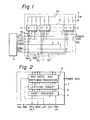
- Figure 1 is a circuit diagram for a direct drive thermal head
- Fig. 2 is a diagram of a drive circuit shown in Fig. 1.
- the thermal recording head 1 has a plurality of integrated circuits 2, hereinafter referred to as IC-1, IC-2, ... IC-n, which form a drive circuit 3.
- the drive circuit 3 has a shift register 6 which stores picture signals fed from a terminal PIX-IN and which operates in response to a clock signal CLK, as shown in Fig. 2.
- the picture signal PIX includes dot signals corresponding to a desired letter or picture to be recorded.
- the drive circuit 3 also has a latching circuit 8 and switching circuit 9.
- the latching circuit 8 operates in response to a latch signal LAT to control the shift register 6.
- the switching circuit 9 operates in response to enable signals ENB (ENB1, ENB2, ...
- 4 designates a power source +E for supplying a heat generating current to the heat generating resistance 6
- 4' designates a power source V DD for supplying drive current to the drive IC's 2
- 5A a power supply line for the power source 4
- 5B a ground line for the power source 4
- 5C a matrix wiring for supplying control signals for the drive IC's 2
- 5C' a power supply line for the power source 4'
- 5C" a ground line for the power source 4'.
- Numeral 7 designates a control circuit of the thermal head 1.
- the current from the power source 4 flows through the power supply line 5A, a selected heat generating resistance R, driven switching transistors (9),to the grounded line 5B to effect a desired printing.
- the construction per se mentioned above is known).
- the present invention is addressed to an internal construction of the thermal recording head 1.
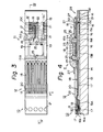
- Figs. 3 through 6 are diagrams illustrating embodiments of the thermal recording head (thermal head) of the present invention.
- Wiring components 15A, 15B, 15C, 15C', and 15C" shown below in Figs. 3 to 6 correspond to 5A, 5B, 5C, 5C', and 5C" in Figs. 1 and 2, respectively.
- Figs. 3 and 4 show a thermal head 10 of a first embodiment of the present invention.
- a resistor protecting film 22, a protecting layer 26, and a heat-resistant protecting resin 27, shown in Fig. 4 are removed, and, practically, the structure is expanded in the direction of arrow P in the rectangular form.
- Figs. 3 show a thermal head 10 of a first embodiment of the present invention.
- a resistor protecting film 22, a protecting layer 26, and a heat-resistant protecting resin 27, shown in Fig. 4 are removed, and, practically, the structure is expanded in the direction of arrow P in the rectangular form.
- reference numerals 11, 12, 13, 14, 15, 16, 17, 18, 19, and 20 represent a multi-layer wiring portion, a heat-generating portion, an alumina substrate, a high-melting-point glaze layer, a first conductor layer, a first insulator layer, a heat-generating resistor layer, a second conductor layer, a driver IC (active element) and a heat-generating point (heat-generating element or heat radiative element), respectively.
- the present embodiment roughly comprises the multi-layer wiring portion 11 loaded with driver IC's 19 and the heat-generating portion 12 on which heat-generating points 20 are formed.
- the alumina substrate 13 is a plate composed of about 97% alumina and has a rectangular shape (the longitudinal direction agrees with the direction of arrow P).
- the high-melting-point glaze layer 14, i.e., heat insulating layer, having a high heat resistance is formed in advance below the resistor layer 17 on which the heat-generating points 20 are formed, that is, on the substrate 13 in the portion corresponding to the resistor layer 17, to prevent heat transmission from the heat generating element 20 to the substrate 13.
- This first conductor layer is patterned and formed when there are printed a logic power source supply line (V DD ) 15C', a logic ground line 15C", a head common electrode (power supply electrode) 15A, a power ground line (earth line) 15B, a connection terminal 15D, and matrix wiring electrodes (controlling electrodes, i.e., signal lines) 15C of an input line where the conductor resistance should be reduced because a large electric current flows.
- the first conductor layer 15 may be formed of a thick film of Au or Ag-Pd instead of the above-mentioned thick film of Cu.
- the first insulator layer 16 is formed on the first conductor layer 15 in the form of a glass thick film having exposed portions, i.e., throughholes or via- holes 21 by using a glass paste comprising a binder capable of being sintered in an inert gas (e.g., N 2 ) atmosphere containing a high density oxygen content.
- an inert gas e.g., N 2
- throughholes 21 should be formed very precisely so as to connect the upper and lower conductor layers (15 and 18).
- This glass thick film 16 comprises at least two glass layers.
- a filler-containing crystalline glass layer for a thick film is formed as a first glass layer 16a by printing, and then a vitrous (amorphous) glass layer is laminated as a second glass layer 16b on the first glass layer 16a by printing, and these two glass layers are integrated to form the glass thick layer 16.
- a very smooth surface (top surface) is formed by the second glass layer 16b which has excellent flowability when heated.
- Through holes 21 of the first and second glass layers are formed at the time of printing.
- the diameter of the throughholes 21 of the second glass layer are originally slightly larger than the diameter of the throughholes 21 of the first glass layer, in view of the flowability of the second glass layer 16b, so that when heated the throughholes 21 of the first and second glass layer become substantially identical to each other, resulting in a formation of precise throughholes.
- the upper and lower conductor layers (15 and 18) can be firmly connected to each other.
- the first insulator layer also may be formed according to a method different from the above-mentioned method. More specifically, the first glass layer 16amay be formed byusing an amorphous glass having a high softening point, and the second glass layer 16b may be formed by using an amorphous glass having a softening point lower than that of the first glass layer 16a. Also, in this case, the same effects as described above can be similarly attained.
- first insulator layer 16 comprising a first glass layer of a crystalline glass and a second glass layer of an amorphous glass
- a first glass layer 16a is formed by repeating two times the printing and sintering of a filler-incorporated crystalline glass paste capable of being sintered at 600°C by using a 325-mesh screen.
- a second glass layer 16a having throughholes having a minimum diameter of 250 ⁇ m and also having a very smooth surface (top surface) is formed by conducting once the printing and sintering of an amorphous glass paste capable of being sintered at 600°C by using a 325-mesh screen.
- Both the glass layers 16a and 16b are integrally laminated to form a first insulator layer 16.
- the exposed surface of the first conductor layer 15 is oxidized, so that oxide is formed.
- the substrate having thereon the first conductor layer 15 and the glass insulator layers 16a and 16b is dipped or immersed in an organic solvent containing an organic acid, such as carbolic acid, hydroxy acids, or carboxylic acids, or a mixture thereof, so that the oxide is activated and removed.
- the organic solvent used is preferably selected from the group of halogenated hydrocarbons, and aromatic hydrocarbons.
- the organic acid is used in the organic solvent in an amount of 3 to 50% by weight of the total weight.
- the density of oxygen contained in the inert gas atmosphere is preferably 200 to 5000 ppm.
- a heat-generating resistor layer 17 is formed as a thin film on the first insulator layer 16.
- Ta 2 N is deposited in a thickness of about ° 300 A by the magnetron sputtering method.
- a second conductor layer 18 is formed as a Cr-Cu-Cr thin film on the heat-generating resistor layer 17.
- Cr is first ° deposited in a thickness of 300 A, Cu is then deposited ° in a thickness of 5000 A on the deposited Cr, and o finally Cr is again deposited in a thickness of 300 A on the deposited Cu, whereby a Cr-Cu-Cr thin film is formed.
- the logic power source supply line, the logic ground line, the power ground line and the like are formed on the first conductor layer 15, and therefore, from the viewpoint of designing, the present embodiment is advantageous in that a fine pattern alone can be arranged on the second conductor layer 18 at a high efficiency.
- the Ta 2 N layer is removed between patterned conductors of Cr-Cu-Cr. Then, the resist is peeled, and for forming heat-generating points (heat-generating elements) 20, a resist is formed on the entire surface again, and a resist pattern opened only in resistor windows (corresponding to heat-generating points 20) is formed by baking.
- the Cr-Cu-Cr layer (second conductor layer 18) in the above-mentioned openings is removed by etching to form heat-generating points 20, that is, a thin film resistor.
- the second conductor layer 18 may be formed by using a single layer or multi-layer of Al, NiCr-Au-Cr, Al(Si), Ti-Pd-Au, Ni-Au, NiCr, Cr, W, Ta, Cu, Ti, Ni, W-Al, Pd, or Au thin film instead of the above-mentioned Cr-Cu-Cr.
- the exposed surface of this Cu should be plated with Ni to protect the Cu surface from the etching medium used. That is, the exposed Cu surfacema(y be also etched if it is not covered by such Ni plating.
- the Ni plating shown at 50 in Fig. 4 is formed after the glass insulator layers 16a and 16b are formed.
- reference numeral 22 represents a resistor-protecting film (anti-abrasive layer) of the Si0 2 -Ta 2 O 5 ⁇ SiO 2 type, and this protecting film 22 is formed in a thickness of, for example, about 4 ⁇ m, by RF (Radio Frequency) sputtering.
- the driver IC (active element) 19 is loaded and secured onto the second conductor layer 18 by using a conductor adhesive (electrically conductive die-bonding resin) 23 according to the die-bonding method.
- an Ni-Au plating layer is previously deposited on the second conductor layer 18 (for example, after etching and removal of the Cr of the bonding pad portion, electrolytic plating is carried out).
- Heat compression Au-to-Au wire bonding is carried out by using a bonding wire 25 (for example, an Au wire) to electrically connect the driver IC 19.
- a bonding wire 25 for example, an Au wire
- the thermal head can be designed so that the driver IC and the like are not wire-bonded to an organic insulator which is mechanically and thermally weak, such as a polyimide resin, and therefore, a multi-layer structure having a very high reliability can be realized.
- reference numeral 26 represents a protecting layer for the driver IC 19, which is formed of a silicone type resin. According to the above-mentioned procedures, the driver IC type thermal head is substantially constructed.
- alumina substrate 11 is secured and loaded onto a rectangular heat sink (not shown), and an external terminal (not shown) is formed on this heat sink to complete fabrication of a driver IC type thermal head.
- reference numerals 27 and 28 represent a heat-resistant protecting resin and a terminal portion, respectively.
- thin film layers and thick film layers are appropriately combined, and the multi-layer structure is formed by skillfully utilizing the merits of these layers.
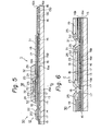
- Figure 5 is a cross-sectional view of a thermal head 30 of a second embodiment of the present invention (corresponding to Fig. 4 of the above mentioned first embodiment), and Fig. 6 is a view showing the section taken along the line VI-VI in Fig. 5 (corresponding to the view showing the section taken along the direction of arrow P in Fig. 3).
- Figs. 5 and 6 members and portions identical or corresponding to the members and portions in Figs. 3 and 4 are indicated by the same reference numerals as in Figs. 3 and 4.
- reference numerals 11, 12, 13, 14, 15, 16, 17, 18, 19, 20, 21, 22, 23, 24, 25, and 26 represent a multi-layer wiring portion, a heat-generating portion, an alumina substrate, a high-melting-point glaze layer, a first conductor layer, a first insulator layer, a heat-generating resistor layer, a second conductor layer, a driver IC (active element), a heat-generating point (heat-generating element), a throughhole, a resistor protecting layer (anti-abrasive anti-oxidation layer), a conductor adhesive (electrically conductive die-bonding resin), an Ni-Au plating layer, a bonding wire (Au wire), and a protecting layer for the driver IC 19, respectively.
- These members and portions are formed substantially in the same manner as in the above-mentioned first embodiment. Accordingly, explanation of these members and portions is omitted.
- Reference numerals 31 and 32 represent a second insulator layer and a third conductor layer, respectively.
- the main difference of the present embodiment from the first embodiment resides in that the second insulator layer 31 and third conductor layer 32 are interposed between the second conductor layer 18 and the driver IC 19.
- a small driver IC is used, wiring is ordinarily completed up to the second conductor layer 18 as in the above-mentioned first embodiment.
- pads on the IC are often distributed (all four edges of the IC) and arranged on the four peripheral portions. Where an IC having such pad arrangement and size is loaded, a certain third conductor layer 32 becomes necessary.
- an example of a driver IC-loaded thermal head having a multi-layer wiring portion 11 including such a third conductor layer 32 is constructed.
- a variety of large driver IC's having different pad arrangements have recently been developed. For example, there can be mentioned driver IC's where pads are arranged only on two confronting peripheral portions. Where a driver IC of this type is loaded, the third conductor layer 32 is not necessary, and multi- layer wiring is completed up to the first conductor layer 18 as in the above-mentioned first embodiment.
- the second insulator layer 31 is formed as a thick film on the second conductor 18 by using an organic insulator such as a polyimide resin.
- this second insulating layer 31 composed of a polyimide resin is formed in the following manner.
- a polyimide resin has a poor thixotropic property and hence, a low printability.
- an inorganic or organic powdery filler is incorporated into a polyimide resin so as to improve the thixotropic property, and the filler-incorporated polyimide resin is screen-printed to form the second insulator layer 31.
- the second insulator layer 31 is formed as a thick film having a thickness of about 15 pm.
- the third conductor layer 32 is formed as a thin film on the second insulator layer 31.
- this third conductor layer 32 is formed in the following manner. A Cr layer having a 0 thickness of 300 A is first formed on the entire surface by the vacuum deposition of Cr or the like means, and a Cu layer having a thickness of 1 ⁇ m is formed on the Cr layer. Then, this thin layer is patterned according to a method similar to the method adopted for formation of the second conductor layer 18, whereby the third conductor layer 32 is formed.
- the driver IC 19 is loaded and secured to the third conductor layer 32 according to the same method as adopted in the first embodiment.
- the present embodiment is different from a previously proposed thin film multi-layer wiring structure constructed by using only a polyimide resin or the like for example in the point that since the wiring is mainly constructed by the first and second conductor layers (15 and 18), the wiring by the third conductor layer 32 can be simplified, with the result that the rejection rate of patterning can be reduced.
- Other effects of the present embodiment are substantially the same as those attained in the first embodiment.
- the multi-layer wiring portion is constructed by using a conductor composed mainly of Cu. This is because Cu is cheap and has a high electric conductivity (low conductor resistance) and a high heat resistance.
- the material of the heat-generating resistor 17 and the material of the protecting film 22 are not limited to the above-mentioned Ta 2 N and Si02-Ta205 ⁇ Si02 , but other appropriate materials can be used.
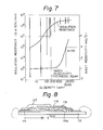
- Figure 7 shows experimental results of characteristics of the ratios of 0 2 density in the N 2 atmosphere for firing the glass paste to the insulation resistance between the upper thin-film conductor layer and the lower thick-film conductor layer and also to the sheet resistivity of the thick film conductor layer.
- the experiments were carried out by using a test sample as shown in Fig. 8, in which a Cu thick film conductor layer 115 which can be fired at a nominal firing temperature of 600°C was formed on the 96% alumina substrate 113.
- Crystalline glass 116a which can be fired at a nominal firing temperature of 600°C was printed and fired twice by using a 325 mesh stainless screen, and then vitrous glass 116b was printed and fired on the first glass layer 116a by using the 325 mesh stainless screen.
- an upper thick film conductor layer 118 of Cr-Cu was formed on the glass layer 116b.
- the upper conductor layer 118 was patterned by a photolithography process and then coated with a protective layer 127 of silicone resin.
- the initial insulation resistance between the thick-film conductor layer 113 and the thin-film conductor layer 118 was measured one minute after a voltage of 50 V was applied, in comparison with the variation of 0 2 density at the so-called a burn out zone of the firing furnace.
- the sheet resistivity of the thick-film conductor layer was also measured.
- the upper limit of the sheet resistivity for achieving desired characteristics of the Cu thick-film conductor layer is (m ⁇ per square) 3 m ⁇ / ⁇ (m ⁇ per square). This fact results in the condition that the 0 2 density should be below 5000 ppm.
- Figure 9 shows experimental results of a relationship between the throughhole resistance and the 0 2 density at the burn-out zone, in the course of firing the glass paste.
- Various organic acid-containing solvents were used to remove the oxide formed on the thick-film conductor layer.
- A shows a known solvent which contains 4% by weight phosphoric acid
- B a solvent of orthodichlorobenzene which contains no organic acid
- C shows no surface treatment, i.e., no step for removal of the oxide.
- D shows an embodiment of the present invention, in which a solvent of orthodichlorobenzene contains 20% carbolic acid by weight and 20% ABS (Alkylbenzene Sulphonate) as a surface-active agent.
- a solvent of orthodichlorobenzene contains 20% carbolic acid by weight and 20% ABS (Alkylbenzene Sulphonate) as a surface-active agent.
- D gave the best result for decreased throughhole resistance. This is because the oxide of Cu and the glass containing Pb can be
- Figure 10 shows experimental results of a relationship between the time of surface treatment (time of immersion of substrate in the solvent) and the intensity of adhesion of Cu thick-film layer to the substrate.
- A shows the solvent of 4% phosphoric acid containing no embodiment organic acid, according to a known process.
- D shows an embodiment of present invention in which the solvent of orthodichlorobenzene contains 20% carbolic acid and 20% ABS.
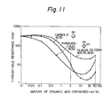
- Figure 11 shows experimental results of the amount (weight %) of the organic acid contained in the solvent in relation to the throughhole resistance.
- the thick-film Cu layer was fired in the N 2 atmosphere containing 700 ppm of 0 2 . Copper oxide about 5000 A in thickness was formed on the throughholes of the exposed Cu surface.
- Three kinds of organic acid, i.e., carbolic acid ( ), pyrocatechuic acid (o-o), and glacial acetic acid were dissolved in the solvent of orthodichlorobenzene containing the ABS surface-active agent. The amounts of organic acids were changed.
- the thin-film conductor layer was formed after the surface treatment for removal of the copper oxide was carried out by immersion in three kinds of solvents containing three kinds of organic acids. The throughhole resistance was then measured.
- the surface-active agent i.e., ABS
- the surface-active agent i.e., ABS
- the thermal recording head of the present invention can be easily fabricated by appropriately combining thick film or thin film conductor layers and thick film insulator layers, forming the first insulator layer as a glass thick film and skillfully utilizing the merits of the thick and thin films. Moreover, the yield can be increased and the manufacturing cost can be reduced. Still further, high-density wiring, high printing speed, and high quality printed letters (high resolving degree) can be realized, and the reliability and performance can be improved.
Landscapes
- Engineering & Computer Science (AREA)
- Manufacturing & Machinery (AREA)
- Multimedia (AREA)
- Signal Processing (AREA)
- Electronic Switches (AREA)
- Parts Printed On Printed Circuit Boards (AREA)
Abstract
Description
- The present invention relates to a thermal recording head to be used for a thermal or heat transfer printer or facsimile. More particularly, the present invention relates to a multi-layer wiring structure of a film type thermal recording head provided with active elements, such as driver integrated circuits (IC's), at a high density.
- The present invention also relates to a process for manufacturing a wiring substrate which can be advantageously used for a thermal recording head.
- A thermal recording head (thermal head) of the above type ordinarily comprises a number of heat-generating parts (heat-generating elements) arranged in a line-dot pattern or matrix, each heat-generating part including a dot formed of a heat-generating resistor (resistor film) and a conductor (film) connected thereto. For example, in the line-dot arrangement, if a recording paper has, for example, a size A4, and the density of the heat-generating parts is 8 lines/mm, about 1728 heat-generating dots are linearly arranged as a whole. Accordingly, in the thermal head of this type, high-density wiring is required for supplying electricity to these heat-generating parts, and therefore, a multi-layer wiring structure becomes necessary. In the of an IC type thermal recording head for use with A4 size recording paper, the number of heat generating dots is, for example, 1728 as mentioned above, and the power voltage (designated by +E in Fig. 1) is 12V. In this kind of thermal head, if the heat generating dots are divided into four groups to be driven, when all the dots are driven,namely when a recording electric current is supplied to all the dots, 50 mA of the current is supplied to each dot at most, but a large current of about 22A is supplied to the power supply lines. That is, a large current flows in the power supply lines, in comparison with each heat generating dot in which only a relatively small current flows.
- A multi-layer wiring structure may be a thick film type (comprising a thick film conductor layer and a thick film insulator layer) or a thin film type (comprising a thin film conductor layer and a thin film separator layer). The former type is advantageous in that fabrication is easy, the manufacturing cost is cheap, the yield is high, and the reliability is high, but is defective in that the printed letter quality (the deviation of the resistance among dots and the resolving degree) is poor and the material cost is high (Au metal films should be used because of various limitations). The latter type is unsatisfactory in several points, but has the advantage of good quality printed letters (the deviation of the resistance among dots or the resolving degree). Accordingly, thin film type thermal heads are use to a great extent at present.
- The wiring pattern of the thermal head of this type is typically divided into a diode matrix type and a driver IC-loaded type. Because of the wiring characteristics, the printing speed of the latter type is higher than that of the former, and thus the latter type has an advantage in this point. Accordingly, as means for simultaneously obtaining a good quality printed letter and a high printing speed, a thin film thermal head of the driver IC type has attracted attention, and investigations have been made on thermal heads of this type. Nevertheless, there are still problems with thermal heads of this type, especially for the multi- layer structure for multi-layer wiring, as described in the following text.
- As pointed out above , high-density multi-layer wiring is necessary for a driver-loaded type thermal head provided with IC's and the like at a high density. In the conventional thin-film thermal heads of this type, the multi-layer structure for multi-layer wiring is constructed by laminating thin films. More specifically, this multi-layer structure is formed by alternately laminating a thin film conductor layer and a thin film insulator layer of an organic material such as a polyimide resin on a substrate composed of alumina or the like by vacuum deposition or the like. Although conventional thin film-typethermal heads fabricated in the above-mentioned manner are advantageous in that the printed letter quality is high and the printing speed is high, they still involve the following problems.
- (1) Since pinholes are readily formed in a thin film of a polyimide resin and short circuits are often formed in insulation-required portions between conductors, the yield in the production process is very low. Accordingly, the number of layers is practically limited to two (the larger the number of layers, the lower the yield), when a thin film of a polyimide resin is used. Moreover, the process for the preparation of a polyimide resin is complicated, and hence, polyimide resin films are expensive.
- (2) For the reasons set forth in (1) above, the manufacturing cost is increased and thus the cost of the thermal heads is increased.
- (3) Since the conductor layer is in the form of a thin film, the conductor.resistance is high. Ac- cordingly, a special treatment is necessary for a power source supply line or power ground line (earth line) where a large electric current flows. For example, the conductor resistance is reduced by subjecting such a line to a plating treatment (the conductor is thickened) or to a partial vacuum deposition treatment, or the conductor resistance is reduced by complicating a pattern of the thin film and broadening the width of the pattern. Accordingly, where a thermal head is constructed by performing the above-mentioned special or additional treatment, designing of multi-layer wiring is very difficult. Moreover, the thermal head is poor in general-purpose characteristics. Namely multi-layer wiring of a (standard), thermal head of a different type cannot be utilized for the present thermal head, and multi-layer wiring suitable for this thermal head must be especially designed.
- In another conventional technique, in order to obviate the problems of the above-mentioned conventional technique, a portion including a terminal part where a large electric current flows is constructed by using a separately formed flexible printed plate. However, this flexible printed plate is very expensive and thus the manufacturing cost is increased, and therefore, this conventional technique is not satisfactory from the practical viewpoint.
- According to still another conventional technique, a driver IC-loaded portion of multi-layer wiring is formed having a thick film multi-layer structure, and a heat-generating dot portion is formed having a thin film structure, and both portions are electrically connected to each other by using a bonding wire or the like. In this case, however, the density of electrc connecting points between the two portions is very high and the number of these electric connecting points is drastically increased (as pointed out hereinbefore, 1728 points for A4 recording paper), also no suitable connecting method is known and the reliability of the connecting points is extremely low. Therefore, this conventional technique cannot be practically applied. Furthermore, even if this conventional technique is (number of manufacturing.processes) practically carried out, the step number/is increased and thus the manufacturing cost is increased.
- An embodiment of the present invention can solve the above-mentioned problems of the conventional techniques and provide a thermal recording head of the thin film type including a thin film resistor, in which a multilayer structure of a multi-layer wiring portion provided with active elements (such as driver IC's) at a high density can be fabricated very easily in a high yield, high-density wiring, high printing speed and high printed letter quality can be realized, and the manufacturing cost can be reduced. An embodiment of the present invention can provide a simple and inexpensive wiring substrate which has a high/electrical property and which can be particularly advantageously used for a thermal recording head.
- An embodiment of the present invention :can provide a process for manufacturing a wiring substrate which is free from the drawbacks mentioned above.
- According to the present invention, there is provided a thermal recording head having a multi-layer wiring structure provided with active elements at a high density, which comprises a substrate, a first conductor layer formed of a thick film and arranged on the substrate, a first insulator layer formed of a glass thick film and arranged on the first conductor layer, a heat-generating resistor layer formed of a thin film and arranged on the first insulator layer, a second conductor layer formed of a thin film and arranged on the resistor layer, and active elements arranged on the second conductor layer.
- Moreover, in accordance with the present invention, there is provided a thermal recording head having a multi-layer wiring structure provided with active elements at a high density, which comprises a substrate, a first conductor layer formed of a thick film and arranged on the substrate, a first insulator layer formed of a glass thick film and arranged on the first conductor layer, a heat-generating resistor layer formed of a thin film and arranged on the first insulator layer, a second conductor layer formed of a thin film and arranged on the resistor layer, a second insulator layer formed of a thick film and arranged on the second conductor layer, a third conductor layer formed of a thin film and arranged on the second insulator layer, and active elements arranged on the third conductor layer.
- According to another aspect of the present invention, there is provided a thermal recording head comprising an insulation substrate having thereon a heat generating resistor pattern made of a thin-film resistor, a predetermined electrode pattern having a common power supply electrode pattern portion and a common grounded electrode pattern portion, for supplying the power to the resistor pattern, a controlling electrode pattern portion, and switching means for controlling the supply of the power to the resistor pattern. The electrode pattern is made of a thick-film copper paste by a printing process. The switching means is controlled by the controlling electrode pattern portion.
- According to still another aspect of the present invention, there is also provided a process for manufacturing a wiring substrate for a thermal recording head, comprising forming a lower layer of a first conductor pattern of a copper thick-film by applying and firing a copper paste on an insulation substrate; forming a glass insulator on the lower layer by applying a glass paste onto the first conductor pattern so that at least a part of the conductor pattern is exposed, and then firing the glass paste in an inert gas atmosphere which contains a high density content of oxygen; removing oxide formed on the exposed surface of the first conductor pattern; and forming an upper layer of a second conductor pattern, which is electrically connected to the exposed surface of the first conductor pattern, on the glass insulator.
- Reference is made, by way of example, to the accompanying drawings, in which:
- Fig. 1 is a circuit diagram of a direct drive thermal head to which the present inventionmay be applied;
- Fig. 2 is a diagram of a drive circuit shown in Fig. 1;
- Fig. 3 is a schematic partial plan view showing _a. first embodiment of the thermal recording head of the present invention, but in which the resistor protecting film, protecting layer and heat-resistant protecting resin shown in Fig. 4 are removed; Fig. 4 is a cross-sectional view showing the section taken along the line IV-IV-IV-IV in Fig. 3; Fig. 5 is a cross-sectional view of a second embodiment of the present invention, corresponding to Fig. 4;
- Fig. 6 is a view showing the section taken along the line VI-VI in Fig. 5;
- Fig. 7 is a diagram showing experimental results for the relationship of 0--density of the inert gas atmosphere, in which the glass paste is fired, to the insulation resistance between the upper thin-film conductor layer and the lower thick-film conductor layer, and also to the sheet resistivity of the Cu thick-film conductor layer;
- Fig. 8 is a schematic sectional view of a test sample used in the experiments;
- Fig. 9 is a diagram of experimental results showing a relationship between the 02 density and the throughhole resistance, in relation to various kinds of solvent in which the substrate is to be dipped to remove the copper oxide;
- Fig. 10 is a diagram of experimental results showing a relationship between the type of surface treatment, i.e., the time of immersion in the solvent and the intensity of the adhesion of the Cu thick-film layer onto the substrate, in relation to the kinds of the solvent; and
- Fig. 11 is a diagram of experimental results showing the relationship between the amount of organic acid to be contained in the solvent and the throughhole various resistance, in relation to kinds of organic acids.
- Figure 1 is a circuit diagram for a direct drive thermal head, and Fig. 2 is a diagram of a drive circuit shown in Fig. 1.
- The
thermal recording head 1 has a plurality of integratedcircuits 2, hereinafter referred to as IC-1, IC-2, ... IC-n, which form adrive circuit 3. Thedrive circuit 3 has ashift register 6 which stores picture signals fed from a terminal PIX-IN and which operates in response to a clock signal CLK, as shown in Fig. 2. The picture signal PIX includes dot signals corresponding to a desired letter or picture to be recorded. Thedrive circuit 3 also has alatching circuit 8 and switchingcircuit 9. Thelatching circuit 8 operates in response to a latch signal LAT to control theshift register 6. Theswitching circuit 9 operates in response to enable signals ENB (ENB1, ENB2, ... ENBn) to control the latchingcircuit 8 in such a manner that the dot signals are moved at one time to acommon conductor 4 through heat generating resistors R. Namely, 4 designates a power source +E for supplying a heat generating current to theheat generating resistance 6; 4' designates a power source VDD for supplying drive current to the drive IC's 2; 5A a power supply line for thepower source 4; 5B a ground line for thepower source 4; 5C a matrix wiring for supplying control signals for the drive IC's 2; 5C' a power supply line for the power source 4'; and 5C" a ground line for the power source 4'.Numeral 7 designates a control circuit of thethermal head 1. The current from thepower source 4 flows through thepower supply line 5A, a selected heat generating resistance R, driven switching transistors (9),to the groundedline 5B to effect a desired printing. (The construction per se mentioned above is known). The present invention is addressed to an internal construction of thethermal recording head 1. - Figs. 3 through 6 are diagrams illustrating embodiments of the thermal recording head (thermal head) of the present invention.
-
Wiring components - Figs. 3 and 4 show a
thermal head 10 of a first embodiment of the present invention. In Fig. 3, aresistor protecting film 22, a protectinglayer 26, and a heat-resistant protectingresin 27, shown in Fig. 4, are removed, and, practically, the structure is expanded in the direction of arrow P in the rectangular form. In Figs. 3 and 4,reference numerals multi-layer wiring portion 11 loaded with driver IC's 19 and the heat-generatingportion 12 on which heat-generatingpoints 20 are formed. Thealumina substrate 13 is a plate composed of about 97% alumina and has a rectangular shape (the longitudinal direction agrees with the direction of arrow P). The high-melting-point glaze layer 14, i.e., heat insulating layer, having a high heat resistance is formed in advance below theresistor layer 17 on which the heat-generatingpoints 20 are formed, that is, on thesubstrate 13 in the portion corresponding to theresistor layer 17, to prevent heat transmission from theheat generating element 20 to thesubstrate 13. Thefirst conductor layer 15 is a thick film of Cu (copper) formed by screen printing with a Cu (copper) paste capable of being sintered in an inert gas (e.g., N2 = nitrogen) atmosphere, subsequent preliminary drying, and sintering in a conveyer type nitrogen furnace. This first conductor layer is patterned and formed when there are printed a logic power source supply line (VDD) 15C', alogic ground line 15C", a head common electrode (power supply electrode) 15A, a power ground line (earth line) 15B, aconnection terminal 15D, and matrix wiring electrodes (controlling electrodes, i.e., signal lines) 15C of an input line where the conductor resistance should be reduced because a large electric current flows. By thus constructing thefirst conductor layer 15 by a thick film of Cu, the area resistance (sheet resistivity) can be reduced to less than about 1/10 of the sheet resistivity in a conventional thin film conductor, and simultaneously, the manufacturing cost can be reduced (because the preparation step is simple). Note, thefirst conductor layer 15 may be formed of a thick film of Au or Ag-Pd instead of the above-mentioned thick film of Cu. Then, thefirst insulator layer 16 is formed on thefirst conductor layer 15 in the form of a glass thick film having exposed portions, i.e., throughholes or via-holes 21 by using a glass paste comprising a binder capable of being sintered in an inert gas (e.g., N2) atmosphere containing a high density oxygen content. In thisfirst insulator layer 16,throughholes 21 should be formed very precisely so as to connect the upper and lower conductor layers (15 and 18). For this purpose, the following contrivance is made in the present embodiment. This glassthick film 16 comprises at least two glass layers. A filler-containing crystalline glass layer for a thick film is formed as afirst glass layer 16a by printing, and then a vitrous (amorphous) glass layer is laminated as asecond glass layer 16b on thefirst glass layer 16a by printing, and these two glass layers are integrated to form the glassthick layer 16. A very smooth surface (top surface) is formed by thesecond glass layer 16b which has excellent flowability when heated. Throughholes 21 of the first and second glass layers are formed at the time of printing. Preferably, the diameter of thethroughholes 21 of the second glass layer are originally slightly larger than the diameter of thethroughholes 21 of the first glass layer, in view of the flowability of thesecond glass layer 16b, so that when heated thethroughholes 21 of the first and second glass layer become substantially identical to each other, resulting in a formation of precise throughholes. Thus, the upper and lower conductor layers (15 and 18) can be firmly connected to each other. By constructing the first insulatinglayer 16 by the thick glass film having the above-mentioned structure, there can be obtained a surface (top surface) having an excellent smoothness and a good insulating property. Moreover, formation of pinholes can be prevented substantially completely, and the yield can be improved. The very smooth face (top surface) makes it easier to form a fine pattern of a thin film thereon and improves the quality of this thin film. Incidentally, the first insulator layer also may be formed according to a method different from the above-mentioned method. More specifically, the first glass layer 16amay be formed byusing an amorphous glass having a high softening point, and thesecond glass layer 16b may be formed by using an amorphous glass having a softening point lower than that of thefirst glass layer 16a. Also, in this case, the same effects as described above can be similarly attained. An example of formation of the above-mentionedfirst insulator layer 16 comprising a first glass layer of a crystalline glass and a second glass layer of an amorphous glass will now be described. At first, afirst glass layer 16a is formed by repeating two times the printing and sintering of a filler-incorporated crystalline glass paste capable of being sintered at 600°C by using a 325-mesh screen. Then, asecond glass layer 16a having throughholes having a minimum diameter of 250 µm and also having a very smooth surface (top surface) is formed by conducting once the printing and sintering of an amorphous glass paste capable of being sintered at 600°C by using a 325-mesh screen. Both the glass layers 16a and 16b are integrally laminated to form afirst insulator layer 16. - In the course of firing the glass paste in an inert gas atmosphere containing a high density oxygen content, the exposed surface of the
first conductor layer 15 is oxidized, so that oxide is formed. To remove the oxide, the substrate having thereon thefirst conductor layer 15 and the glass insulator layers 16a and 16b is dipped or immersed in an organic solvent containing an organic acid, such as carbolic acid, hydroxy acids, or carboxylic acids, or a mixture thereof, so that the oxide is activated and removed. The organic solvent used is preferably selected from the group of halogenated hydrocarbons, and aromatic hydrocarbons. Preferably, the organic acid is used in the organic solvent in an amount of 3 to 50% by weight of the total weight. - The density of oxygen contained in the inert gas atmosphere is preferably 200 to 5000 ppm. After the oxide is removed, a heat-generating
resistor layer 17 is formed as a thin film on thefirst insulator layer 16. According to an example of the formation of thisresistor layer 17, Ta2N is deposited in a thickness of about ° 300 A by the magnetron sputtering method. Then, asecond conductor layer 18 is formed as a Cr-Cu-Cr thin film on the heat-generatingresistor layer 17. According to an example of the formation of thesecond conductor layer 18, by vacuum deposition or the like, Cr is first ° deposited in a thickness of 300 A, Cu is then deposited ° in a thickness of 5000 A on the deposited Cr, and o finally Cr is again deposited in a thickness of 300 A on the deposited Cu, whereby a Cr-Cu-Cr thin film is formed. - Cr is deposited as the topmost layer in the
second conductor layer 18 because the adhesion between the resistor-protectingfilm 22 and thisconductor layer 18 is thus improved. Then, pattern baking is carried out by using a negative type resist and only the Cr-Cu-Cr conductor is wet-etched to form a stripe pattern (see Fig. 3 and Fig. 6 described hereinafter). - In the present embodiment, as pointed out hereinbefore, the logic power source supply line, the logic ground line, the power ground line and the like are formed on the
first conductor layer 15, and therefore, from the viewpoint of designing, the present embodiment is advantageous in that a fine pattern alone can be arranged on thesecond conductor layer 18 at a high efficiency. By reactive plasma etching using a CF4-02 type gas, the Ta2N layer is removed between patterned conductors of Cr-Cu-Cr. Then, the resist is peeled, and for forming heat-generating points (heat-generating elements) 20, a resist is formed on the entire surface again, and a resist pattern opened only in resistor windows (corresponding to heat-generating points 20) is formed by baking. Subsequently, the Cr-Cu-Cr layer (second conductor layer 18) in the above-mentioned openings is removed by etching to form heat-generatingpoints 20, that is, a thin film resistor. Note, thesecond conductor layer 18 may be formed by using a single layer or multi-layer of Al, NiCr-Au-Cr, Al(Si), Ti-Pd-Au, Ni-Au, NiCr, Cr, W, Ta, Cu, Ti, Ni, W-Al, Pd, or Au thin film instead of the above-mentioned Cr-Cu-Cr. However, where thesecond conductor layer 18 is formed by using NiCr-Au-Cr and thefirst conductor layer 15 is formed of Cu, the exposed surface of this Cu should be plated with Ni to protect the Cu surface from the etching medium used. That is, the exposed Cu surfacema(y be also etched if it is not covered by such Ni plating. The Ni plating shown at 50 in Fig. 4 is formed after the glass insulator layers 16a and 16b are formed. In this embodiment,reference numeral 22 represents a resistor-protecting film (anti-abrasive layer) of the Si02-Ta2O5·SiO2 type, and this protectingfilm 22 is formed in a thickness of, for example, about 4 µm, by RF (Radio Frequency) sputtering. The driver IC (active element) 19 is loaded and secured onto thesecond conductor layer 18 by using a conductor adhesive (electrically conductive die-bonding resin) 23 according to the die-bonding method. In order to improve the wire bondability, an Ni-Au plating layer is previously deposited on the second conductor layer 18 (for example, after etching and removal of the Cr of the bonding pad portion, electrolytic plating is carried out). Heat compression Au-to-Au wire bonding is carried out by using a bonding wire 25 (for example, an Au wire) to electrically connect thedriver IC 19. As is apparent from the foregoing description, according to thepresent embodiment 10, the thermal head can be designed so that the driver IC and the like are not wire-bonded to an organic insulator which is mechanically and thermally weak, such as a polyimide resin, and therefore, a multi-layer structure having a very high reliability can be realized. Note,reference numeral 26 represents a protecting layer for thedriver IC 19, which is formed of a silicone type resin. According to the above-mentioned procedures, the driver IC type thermal head is substantially constructed. Practically, however, thealumina substrate 11 is secured and loaded onto a rectangular heat sink (not shown), and an external terminal (not shown) is formed on this heat sink to complete fabrication of a driver IC type thermal head. Note, in Fig. 2,reference numerals - As is apparent from the foregoing description, in the present embodiment, thin film layers and thick film layers are appropriately combined, and the multi-layer structure is formed by skillfully utilizing the merits of these layers.
- Figure 5 is a cross-sectional view of a
thermal head 30 of a second embodiment of the present invention (corresponding to Fig. 4 of the above mentioned first embodiment), and Fig. 6 is a view showing the section taken along the line VI-VI in Fig. 5 (corresponding to the view showing the section taken along the direction of arrow P in Fig. 3). In Figs. 5 and 6, members and portions identical or corresponding to the members and portions in Figs. 3 and 4 are indicated by the same reference numerals as in Figs. 3 and 4. Therefore,reference numerals driver IC 19, respectively. These members and portions are formed substantially in the same manner as in the above-mentioned first embodiment. Accordingly, explanation of these members and portions is omitted. -
Reference numerals second insulator layer 31 andthird conductor layer 32 are interposed between thesecond conductor layer 18 and thedriver IC 19. If a small driver IC is used, wiring is ordinarily completed up to thesecond conductor layer 18 as in the above-mentioned first embodiment. However, if a large driver IC having a large current capacitance (or driver LSI) is used, pads on the IC are often distributed (all four edges of the IC) and arranged on the four peripheral portions. Where an IC having such pad arrangement and size is loaded, a certainthird conductor layer 32 becomes necessary. In the present second embodiment, an example of a driver IC-loaded thermal head having amulti-layer wiring portion 11 including such athird conductor layer 32 is constructed. A variety of large driver IC's having different pad arrangements have recently been developed. For example, there can be mentioned driver IC's where pads are arranged only on two confronting peripheral portions. Where a driver IC of this type is loaded, thethird conductor layer 32 is not necessary, and multi- layer wiring is completed up to thefirst conductor layer 18 as in the above-mentioned first embodiment. - Referring to Figs. 5 and 6, the
second insulator layer 31 is formed as a thick film on thesecond conductor 18 by using an organic insulator such as a polyimide resin. For example, this second insulatinglayer 31 composed of a polyimide resin is formed in the following manner. Ordinarily, a polyimide resin has a poor thixotropic property and hence, a low printability. Accordingly, an inorganic or organic powdery filler is incorporated into a polyimide resin so as to improve the thixotropic property, and the filler-incorporated polyimide resin is screen-printed to form thesecond insulator layer 31. In order to improve the insulating property between the conductor layers, thesecond insulator layer 31 is formed as a thick film having a thickness of about 15 pm. Then, thethird conductor layer 32 is formed as a thin film on thesecond insulator layer 31. For example, thisthird conductor layer 32 is formed in the following manner. A Cr layer having a 0 thickness of 300 A is first formed on the entire surface by the vacuum deposition of Cr or the like means, and a Cu layer having a thickness of 1 µm is formed on the Cr layer. Then, this thin layer is patterned according to a method similar to the method adopted for formation of thesecond conductor layer 18, whereby thethird conductor layer 32 is formed. Then, thedriver IC 19 is loaded and secured to thethird conductor layer 32 according to the same method as adopted in the first embodiment. The present embodiment is different from a previously proposed thin film multi-layer wiring structure constructed by using only a polyimide resin or the like for example in the point that since the wiring is mainly constructed by the first and second conductor layers (15 and 18), the wiring by thethird conductor layer 32 can be simplified, with the result that the rejection rate of patterning can be reduced. Other effects of the present embodiment are substantially the same as those attained in the first embodiment. - As is apparent from the foregoing detailed description, in each of the foregoing embodiments, the multi-layer wiring portion is constructed by using a conductor composed mainly of Cu. This is because Cu is cheap and has a high electric conductivity (low conductor resistance) and a high heat resistance. The material of the heat-generating
resistor 17 and the material of the protectingfilm 22 are not limited to the above-mentioned Ta2N and Si02-Ta205·Si02 , but other appropriate materials can be used. - Figure 7 shows experimental results of characteristics of the ratios of 02 density in the N2 atmosphere for firing the glass paste to the insulation resistance between the upper thin-film conductor layer and the lower thick-film conductor layer and also to the sheet resistivity of the thick film conductor layer. The experiments were carried out by using a test sample as shown in Fig. 8, in which a Cu thick
film conductor layer 115 which can be fired at a nominal firing temperature of 600°C was formed on the 96% alumina substrate 113.Crystalline glass 116a which can be fired at a nominal firing temperature of 600°C was printed and fired twice by using a 325 mesh stainless screen, and then vitrous glass 116b was printed and fired on thefirst glass layer 116a by using the 325 mesh stainless screen. Finally, an upper thickfilm conductor layer 118 of Cr-Cu was formed on the glass layer 116b. Theupper conductor layer 118 was patterned by a photolithography process and then coated with aprotective layer 127 of silicone resin. The initial insulation resistance between the thick-film conductor layer 113 and the thin-film conductor layer 118 was measured one minute after a voltage of 50 V was applied, in comparison with the variation of 02 density at the so-called a burn out zone of the firing furnace. The sheet resistivity of the thick-film conductor layer was also measured. - As can be seen from Fig. 7, it was clear that the insulation resistance varied in accordance with the change in 02 density and that the sheet resistivity varied greatly when the 02 density exceeded about 1000 ppm.
- _ - I.t is thought that the upper limit of the sheet resistivity for achieving desired characteristics of the Cu thick-film conductor layer is (mΩ per square) 3 mΩ/□ (mΩ per square). This fact results in the condition that the 02 density should be below 5000 ppm.
- On the other hand it is also thought that the insulation resistance must be above 1O11Ω to ensure reliability of the insulator. From this, it was derived that 02 density should be above 200 ppm. In a known process
- the glass paste is usually fired in an N2 atmosphere containing a
low density 02 below 5 ~ 50 ppm. - Figure 9 shows experimental results of a relationship between the throughhole resistance and the 02 density at the burn-out zone, in the course of firing the glass paste. Various organic acid-containing solvents were used to remove the oxide formed on the thick-film conductor layer. In Fig. 9, A shows a known solvent which contains 4% by weight phosphoric acid, B a solvent of orthodichlorobenzene which contains no organic acid, and C shows no surface treatment, i.e., no step for removal of the oxide. D shows an embodiment of
the present invention, in which a solvent of orthodichlorobenzene contains 20% carbolic acid by weight and 20% ABS (Alkylbenzene Sulphonate) as a surface-active agent. As can be seen from Fig. 9, D gave the best result for decreased throughhole resistance. This is because the oxide of Cu and the glass containing Pb can be weakly etched. - Figure 10 shows experimental results of a relationship between the time of surface treatment (time of immersion of substrate in the solvent) and the intensity of adhesion of Cu thick-film layer to the substrate. A shows the solvent of 4% phosphoric acid containing no embodiment organic acid, according to a known process. D shows an embodiment of present invention in which the solvent of orthodichlorobenzene contains 20% carbolic acid and 20% ABS. As can be seen from Fig 10, according to the present invention, a decrease in the intensity of adhesion of the Cu thick-film layer to the substrate can . be prevented.
- Figure 11 shows experimental results of the amount (weight %) of the organic acid contained in the solvent in relation to the throughhole resistance. The thick-film Cu layer was fired in the N2 atmosphere containing 700 ppm of 02. Copper oxide about 5000 A in thickness was formed on the throughholes of the exposed Cu surface. Three kinds of organic acid, i.e., carbolic acid (), pyrocatechuic acid (o-o), and glacial acetic acid were dissolved in the solvent of orthodichlorobenzene containing the ABS surface-active agent. The amounts of organic acids were changed. The thin-film conductor layer was formed after the surface treatment for removal of the copper oxide was carried out by immersion in three kinds of solvents containing three kinds of organic acids. The throughhole resistance was then measured.

- As can be seen from Fig. 11, when the amounts of organic acids were 3 to 50% by weight, the throughhole resistance could be greatly decreased.
- Finally, it was confirmed that the surface-active agent, i.e., ABS, contained in the solvent is only for improving the surface wetness and can be dispensed with.
- As is apparent from the foregoing description, the thermal recording head of the present invention can be easily fabricated by appropriately combining thick film or thin film conductor layers and thick film insulator layers, forming the first insulator layer as a glass thick film and skillfully utilizing the merits of the thick and thin films. Moreover, the yield can be increased and the manufacturing cost can be reduced. Still further, high-density wiring, high printing speed, and high quality printed letters (high resolving degree) can be realized, and the reliability and performance can be improved.
Claims (20)
Applications Claiming Priority (4)
| Application Number | Priority Date | Filing Date | Title |
|---|---|---|---|
| JP56149/84 | 1984-03-26 | ||
| JP59056149A JPS60199673A (en) | 1984-03-26 | 1984-03-26 | Thermal recording head |
| JP60049816A JPS61208295A (en) | 1985-03-13 | 1985-03-13 | Formation of multi-layer conductor pattern for circuit board |
| JP49816/85 | 1985-03-13 |
Publications (3)
| Publication Number | Publication Date |
|---|---|
| EP0157563A2 true EP0157563A2 (en) | 1985-10-09 |
| EP0157563A3 EP0157563A3 (en) | 1988-10-12 |
| EP0157563B1 EP0157563B1 (en) | 1992-05-20 |
Family
ID=26390272
Family Applications (1)
| Application Number | Title | Priority Date | Filing Date |
|---|---|---|---|
| EP85302032A Expired - Lifetime EP0157563B1 (en) | 1984-03-26 | 1985-03-25 | Thermal recording head and process for manufacturing wiring substrate therefor |
Country Status (5)
| Country | Link |
|---|---|
| US (1) | US4689638A (en) |
| EP (1) | EP0157563B1 (en) |
| KR (1) | KR900002807B1 (en) |
| CA (1) | CA1237019A (en) |
| DE (1) | DE3586065D1 (en) |
Cited By (3)
| Publication number | Priority date | Publication date | Assignee | Title |
|---|---|---|---|---|
| GB2218942A (en) * | 1988-05-27 | 1989-11-29 | Seiko Epson Corp | Thermal print heads |
| WO1990001810A1 (en) * | 1988-08-01 | 1990-02-22 | Siemens Aktiengesellschaft | Functional component of linear design |
| EP0498400A1 (en) * | 1991-02-06 | 1992-08-12 | Rohm Co., Ltd. | Thermal head |
Families Citing this family (9)
| Publication number | Priority date | Publication date | Assignee | Title |
|---|---|---|---|---|
| US5028934A (en) * | 1988-10-31 | 1991-07-02 | Seiko Epson Corporation | Hand-held portable printing system |
| US5066960A (en) * | 1989-04-05 | 1991-11-19 | Sharp | Thermal printing head |
| EP0443339A1 (en) * | 1990-02-21 | 1991-08-28 | Lexmark International, Inc. | Thermal transfer printing head and method for making same |
| US6034706A (en) * | 1996-05-30 | 2000-03-07 | Rohm Co., Ltd. | Head device provided with drive ICS, to which protective coating is applied, and method of forming protective coating |
| JP3169842B2 (en) | 1996-10-07 | 2001-05-28 | セイコーインスツルメンツ株式会社 | Thermal head and method of manufacturing the same |
| US6028619A (en) * | 1997-10-06 | 2000-02-22 | Seiko Instruments Inc. | Thermal head |
| US7149090B2 (en) * | 2001-09-11 | 2006-12-12 | Brother Kogyo Kabushiki Kaisha | Structure of flexible printed circuit board |
| JP5467913B2 (en) * | 2010-04-21 | 2014-04-09 | アルプス電気株式会社 | Thermal head |
| CN111763921A (en) * | 2019-04-01 | 2020-10-13 | 浙江工业大学之江学院 | Manufacturing method of thermal garment material and thermal garment material |
Citations (6)
| Publication number | Priority date | Publication date | Assignee | Title |
|---|---|---|---|---|
| US4241103A (en) * | 1977-05-31 | 1980-12-23 | Nippon Electric Co., Ltd. | Method of manufacturing an integrated thermal printing head |
| JPS5664885A (en) * | 1979-11-02 | 1981-06-02 | Toshiba Corp | Thermosensitive head |
| EP0077546A2 (en) * | 1981-10-19 | 1983-04-27 | Kabushiki Kaisha Toshiba | Thermal recording device |
| EP0079063A2 (en) * | 1981-11-06 | 1983-05-18 | Matsushita Electric Industrial Co., Ltd. | Thermal printing head |
| EP0128760A1 (en) * | 1983-06-09 | 1984-12-19 | Matsushita Electric Industrial Co., Ltd. | Thermal recording head |
| EP0129876A2 (en) * | 1983-06-27 | 1985-01-02 | Teletype Corporation | A thermal print head |
Family Cites Families (2)
| Publication number | Priority date | Publication date | Assignee | Title |
|---|---|---|---|---|
| US3988569A (en) * | 1974-12-16 | 1976-10-26 | Texas Instruments Incorporated | Thermal printhead with memory |
| US4259564A (en) * | 1977-05-31 | 1981-03-31 | Nippon Electric Co., Ltd. | Integrated thermal printing head and method of manufacturing the same |
-
1985
- 1985-03-18 CA CA000476831A patent/CA1237019A/en not_active Expired
- 1985-03-18 US US06/712,713 patent/US4689638A/en not_active Expired - Fee Related
- 1985-03-25 EP EP85302032A patent/EP0157563B1/en not_active Expired - Lifetime
- 1985-03-25 DE DE8585302032T patent/DE3586065D1/en not_active Expired - Fee Related
- 1985-03-26 KR KR1019850001981A patent/KR900002807B1/en not_active IP Right Cessation
Patent Citations (6)
| Publication number | Priority date | Publication date | Assignee | Title |
|---|---|---|---|---|
| US4241103A (en) * | 1977-05-31 | 1980-12-23 | Nippon Electric Co., Ltd. | Method of manufacturing an integrated thermal printing head |
| JPS5664885A (en) * | 1979-11-02 | 1981-06-02 | Toshiba Corp | Thermosensitive head |
| EP0077546A2 (en) * | 1981-10-19 | 1983-04-27 | Kabushiki Kaisha Toshiba | Thermal recording device |
| EP0079063A2 (en) * | 1981-11-06 | 1983-05-18 | Matsushita Electric Industrial Co., Ltd. | Thermal printing head |
| EP0128760A1 (en) * | 1983-06-09 | 1984-12-19 | Matsushita Electric Industrial Co., Ltd. | Thermal recording head |
| EP0129876A2 (en) * | 1983-06-27 | 1985-01-02 | Teletype Corporation | A thermal print head |
Non-Patent Citations (1)
| Title |
|---|
| PATENT ABSTRACTS OF JAPAN, vol. 5, no. 127 (M-83)[799], 15th August 1981; & JP-A-56 64 885 (TOKYO SHIBAURA DENKI K.K.) 02-06-1981 * |
Cited By (5)
| Publication number | Priority date | Publication date | Assignee | Title |
|---|---|---|---|---|
| GB2218942A (en) * | 1988-05-27 | 1989-11-29 | Seiko Epson Corp | Thermal print heads |
| GB2218942B (en) * | 1988-05-27 | 1992-11-11 | Seiko Epson Corp | Thermal print head |
| WO1990001810A1 (en) * | 1988-08-01 | 1990-02-22 | Siemens Aktiengesellschaft | Functional component of linear design |
| EP0498400A1 (en) * | 1991-02-06 | 1992-08-12 | Rohm Co., Ltd. | Thermal head |
| US5278580A (en) * | 1991-02-06 | 1994-01-11 | Rohm Co., Ltd. | Thermal head |
Also Published As
| Publication number | Publication date |
|---|---|
| KR900002807B1 (en) | 1990-04-30 |
| EP0157563B1 (en) | 1992-05-20 |
| EP0157563A3 (en) | 1988-10-12 |
| US4689638A (en) | 1987-08-25 |
| DE3586065D1 (en) | 1992-06-25 |
| CA1237019A (en) | 1988-05-24 |
| KR850006811A (en) | 1985-10-16 |
Similar Documents
| Publication | Publication Date | Title |
|---|---|---|
| US4343833A (en) | Method of manufacturing thermal head | |
| EP0157563B1 (en) | Thermal recording head and process for manufacturing wiring substrate therefor | |
| US4241103A (en) | Method of manufacturing an integrated thermal printing head | |
| US4204107A (en) | Thick-film thermal printing head and method of manufacturing the same | |
| US5041847A (en) | Thermal head | |
| EP0059102B1 (en) | Crossover construction of thermal-head | |
| US4710263A (en) | Method of fabricating print head for thermal printer | |
| EP0744291B1 (en) | Charge plate fabrication process | |
| JP3124870B2 (en) | Thermal head and method of manufacturing the same | |
| JP3824246B2 (en) | Manufacturing method of thermal head | |
| JPH03222760A (en) | Thermal head and manufacture thereof | |
| EP0113950B1 (en) | Method of making a resistance heater | |
| JP3129912B2 (en) | Manufacturing method of thermal head | |
| KR920007534B1 (en) | Thermal printer head | |
| JPH0517864B2 (en) | ||
| JPS60199673A (en) | Thermal recording head | |
| EP0375954B1 (en) | Method of manufacturing printed circuit board | |
| JPS62292456A (en) | Manufacture of thermal head | |
| JPH0147036B2 (en) | ||
| JPS6072749A (en) | Thermal head and manufacture thereof | |
| JPS6052364A (en) | Thermal head and manufacture thereof | |
| JPH0811337A (en) | Thermal printing head | |
| GB2238666A (en) | Hybrid circuit having thick film resistors. | |
| JPH0839855A (en) | Thermal head and production thereof | |
| JPH0832029A (en) | Manufacture of hybrid integrated circuit |
Legal Events
| Date | Code | Title | Description |
|---|---|---|---|
| PUAI | Public reference made under article 153(3) epc to a published international application that has entered the european phase |
Free format text: ORIGINAL CODE: 0009012 |
|
| AK | Designated contracting states |
Designated state(s): DE FR GB IT NL |
|
| PUAL | Search report despatched |
Free format text: ORIGINAL CODE: 0009013 |
|
| AK | Designated contracting states |
Kind code of ref document: A3 Designated state(s): DE FR GB IT NL |
|
| 17P | Request for examination filed |
Effective date: 19881115 |
|
| 17Q | First examination report despatched |
Effective date: 19900927 |
|
| ITF | It: translation for a ep patent filed |
Owner name: INTERPATENT ST.TECN. BREV. |
|
| GRAA | (expected) grant |
Free format text: ORIGINAL CODE: 0009210 |
|
| AK | Designated contracting states |
Kind code of ref document: B1 Designated state(s): DE FR GB IT NL |
|
| PGFP | Annual fee paid to national office [announced via postgrant information from national office to epo] |
Ref country code: FR Payment date: 19920521 Year of fee payment: 9 |
|
| REF | Corresponds to: |
Ref document number: 3586065 Country of ref document: DE Date of ref document: 19920625 |
|
| ET | Fr: translation filed | ||
| PGFP | Annual fee paid to national office [announced via postgrant information from national office to epo] |
Ref country code: GB Payment date: 19930312 Year of fee payment: 9 |
|
| PLBE | No opposition filed within time limit |
Free format text: ORIGINAL CODE: 0009261 |
|
| STAA | Information on the status of an ep patent application or granted ep patent |
Free format text: STATUS: NO OPPOSITION FILED WITHIN TIME LIMIT |
|
| ITTA | It: last paid annual fee | ||
| PGFP | Annual fee paid to national office [announced via postgrant information from national office to epo] |
Ref country code: NL Payment date: 19930331 Year of fee payment: 9 |
|
| 26N | No opposition filed | ||
| PGFP | Annual fee paid to national office [announced via postgrant information from national office to epo] |
Ref country code: DE Payment date: 19930521 Year of fee payment: 9 |
|
| PG25 | Lapsed in a contracting state [announced via postgrant information from national office to epo] |
Ref country code: GB Effective date: 19940325 |
|
| PG25 | Lapsed in a contracting state [announced via postgrant information from national office to epo] |
Ref country code: NL Effective date: 19941001 |
|
| NLV4 | Nl: lapsed or anulled due to non-payment of the annual fee | ||
| GBPC | Gb: european patent ceased through non-payment of renewal fee |
Effective date: 19940325 |
|
| PG25 | Lapsed in a contracting state [announced via postgrant information from national office to epo] |
Ref country code: FR Effective date: 19941130 |
|
| PG25 | Lapsed in a contracting state [announced via postgrant information from national office to epo] |
Ref country code: DE Effective date: 19941201 |
|
| REG | Reference to a national code |
Ref country code: FR Ref legal event code: ST |