EP0492986A2 - Accéléromètre - Google Patents
Accéléromètre Download PDFInfo
- Publication number
- EP0492986A2 EP0492986A2 EP91311803A EP91311803A EP0492986A2 EP 0492986 A2 EP0492986 A2 EP 0492986A2 EP 91311803 A EP91311803 A EP 91311803A EP 91311803 A EP91311803 A EP 91311803A EP 0492986 A2 EP0492986 A2 EP 0492986A2
- Authority
- EP
- European Patent Office
- Prior art keywords
- mass
- support
- sensors
- beams
- movement
- Prior art date
- Legal status (The legal status is an assumption and is not a legal conclusion. Google has not performed a legal analysis and makes no representation as to the accuracy of the status listed.)
- Granted
Links
- 230000001133 acceleration Effects 0.000 claims abstract description 55
- 230000004044 response Effects 0.000 claims abstract description 19
- 239000004065 semiconductor Substances 0.000 claims abstract description 19
- XUIMIQQOPSSXEZ-UHFFFAOYSA-N Silicon Chemical compound [Si] XUIMIQQOPSSXEZ-UHFFFAOYSA-N 0.000 claims abstract description 17
- 229910052710 silicon Inorganic materials 0.000 claims abstract description 17
- 239000010703 silicon Substances 0.000 claims abstract description 17
- 239000000463 material Substances 0.000 claims description 33
- 239000004020 conductor Substances 0.000 claims description 19
- 238000004519 manufacturing process Methods 0.000 claims description 4
- 230000035945 sensitivity Effects 0.000 description 10
- 230000006378 damage Effects 0.000 description 5
- 230000006835 compression Effects 0.000 description 4
- 238000007906 compression Methods 0.000 description 4
- 230000009467 reduction Effects 0.000 description 4
- 208000027418 Wounds and injury Diseases 0.000 description 3
- 208000014674 injury Diseases 0.000 description 3
- 230000008859 change Effects 0.000 description 2
- 230000000694 effects Effects 0.000 description 2
- 238000000034 method Methods 0.000 description 2
- 239000002210 silicon-based material Substances 0.000 description 2
- 230000004308 accommodation Effects 0.000 description 1
- 238000007796 conventional method Methods 0.000 description 1
- 238000013016 damping Methods 0.000 description 1
- 230000007613 environmental effect Effects 0.000 description 1
- 239000011521 glass Substances 0.000 description 1
- 238000011065 in-situ storage Methods 0.000 description 1
- 238000012986 modification Methods 0.000 description 1
- 230000004048 modification Effects 0.000 description 1
- 230000001105 regulatory effect Effects 0.000 description 1
- 230000035939 shock Effects 0.000 description 1
Images


Classifications
-
- G—PHYSICS
- G01—MEASURING; TESTING
- G01P—MEASURING LINEAR OR ANGULAR SPEED, ACCELERATION, DECELERATION, OR SHOCK; INDICATING PRESENCE, ABSENCE, OR DIRECTION, OF MOVEMENT
- G01P15/00—Measuring acceleration; Measuring deceleration; Measuring shock, i.e. sudden change of acceleration
- G01P15/02—Measuring acceleration; Measuring deceleration; Measuring shock, i.e. sudden change of acceleration by making use of inertia forces using solid seismic masses
- G01P15/08—Measuring acceleration; Measuring deceleration; Measuring shock, i.e. sudden change of acceleration by making use of inertia forces using solid seismic masses with conversion into electric or magnetic values
- G01P15/12—Measuring acceleration; Measuring deceleration; Measuring shock, i.e. sudden change of acceleration by making use of inertia forces using solid seismic masses with conversion into electric or magnetic values by alteration of electrical resistance
- G01P15/123—Measuring acceleration; Measuring deceleration; Measuring shock, i.e. sudden change of acceleration by making use of inertia forces using solid seismic masses with conversion into electric or magnetic values by alteration of electrical resistance by piezo-resistive elements, e.g. semiconductor strain gauges
Definitions
- the field of this invention is that of accelerometers, and the invention relates more particularly to silicon accelerometers incorporating piezoresistive sensing means.
- Certain known silicon accelerometers comprise a silicon semiconductor member mounted on a base, the member having a mass mounted on a support by integral beams extending between the support and mass to permit movement of the mass relative to the base in response to an acceleration force. Portions of the semiconductor beam materials are doped to form piezoresistive sensors within the beams for sensing strain in the beams during movement of the mass to provide an output signal from the device corresponding to the acceleration. The sensors are interconnected in a bridge circuit to provide reduction in device sensitivity to off-axis accelerations.
- the beams are arranged to permit selected movement of the mass in response to selected acceleration to provide the accelerometer with desired sensitivity to selected levels of acceleration force while also withstanding injury to the beams during application of the acceleration forces to the beams.
- the strains established in the beams in known accelerometers vary along the lengths of the beams and that the piezoresistive sensors have selected lengths extending along sections of the beams so that the sensors typically respond to the average strain in the beam sections occupied by the sensors rather than to the maximum strain levels in the beams.
- the novel and improved accelerometer device of the invention comprises a semiconductor member of a silicon material or the like.
- One portion of the member comprises a mass which is supported within a opening in a preferably rectangular frame or support portion of the member by at least one and preferably a plurality of integral member beams, thereby to permit movement of the mass relative to the support in response to acceleration of the member.
- the member is formed primarily of a semiconductor material of one conductivity type, and piezoresistive sensors comprising semiconductor material of a second conductivity type are accommodated within the beams for sensing strain established in the beams during movement of the mass to provide an output signal corresponding to the member acceleration.
- each beam has an end secured to the support and an end secured to the mass and has a section of the beam which is tapered to provide the beam section with a high and substantially uniform strain throughout the beam section when the mass moves in response to selected member acceleration.
- each beam has two tapered sections tapering from wider beam parts at the respective beam ends to a narrow beam part nearer the center of the beam. The width of the wider part of each beam section is selected so that the beam material is adapted to withstand the highest strains which are typically encountered in the beam materials at the beam ends where the beams are secured to the relatively larger and stiffer support and mass portions of the semiconductor member.
- each beam section at the end of the taper is selected so that the beam material is subjected to substantially the same high strain in the beam material throughout the length of the tapered beam section during movement of the mass with the selected acceleration.
- the narrower part of the beam is also selected to assure that the strain limits of the beam materials are not exceeded, thereby to also protect the narrow beam part from injury or damage.
- the piezoresistive sensors are then located within the beam sections to be responsive to those high and uniform beam strains. In that way, the accelerometer beams are adapted to withstand selected acceleration forces without excessive strain in any portion of the beams while the piezoresistive sensors are also adapted to be responsive to higher strain levels for selected accelerations, whereby the accelerometer is adapted to display improved sensitivity.
- the piezoresistive sensors are interconnected using conventioned techniques with novel interconnection paths for permitting the interconnection to effect reduction in response of the device to off-axis acceleration forces while also permitting the paths to be formed and accommodated with improved convenience in the devices.
- the device preferably includes a base 12 of a strong, rigid material such as glass or silicon or the like and a semiconductor member 14 formed of a silicon semiconductor material or the like is mounted on the base in any conventional manner. If desired, a cover 16 is secured to the member to provide an environmental seal for the device.
- One portion 18 of the semiconductor member serves as a seismic mass or the like which is supported within an opening 20 in a preferably rectangular frame or support portion 22 of the member by at least one, and preferably by a plurality of, integral member beams 24 to permit movement of the mass 18 relative to the support 22 and base 12 in response to acceleration of the device 10.
- the semiconductor member 14 is primarily formed of the silicon semiconductor material of one conductivity type and portions 26.1-26.8 of the beam materials are doped to provide silicon materials of a second conductivity type to provide piezoresistive sensor means in the beam which are adapted to sense strain in the beam materials to provide an output signal from the device corresponding to the member acceleration in well known manner.
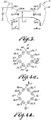
- the beams 24 of the member are provided with a selected configuration as shown particularly in Figure 3 and the proportions of the beams are located with respect to the piezoresistive sensors 26.1-26.8 to provide improved device sensitivity. That is, the beams are preferably provided with a thickness t substantially less than the thickness of the mass 18 and support 22 (see Figure 2) so that the mass is adapted to move toward the base 12 in response to acceleration of the device 10 in a selected direction along a Z axis to develop a high strain in the beam materials at the ends 24.1, 24.2 of the beam where the beams are secured to the relatively thicker and stiffer support and mass portions of the member.
- the beams are also provided with tapered beam sections 24.3, 24.4 as shown so that strain in the beam material is substantially uniform throughout the length of the tapered beam section.
- this taper also provides substantially uniform unit stress in the beam material through the tapered beam section.
- each beam is provided with two tapered sections each of which is adapted to be subjected to substantially uniform unit strain in the beam material in response to device acceleration.
- the wider portions w of the beams at the ends of the beams are selected with respect to the beam thickness so that the beam material is subjected to a sufficiently high strain at the ends of the beams for permitting the piezoresistive sensor 26 to respond to that high strain with an output signal of desired magnitude, the widths w also being selected so that the beams are not fractured at the beam ends when those high strains are established in the beam materials at those locations during device acceleration.
- the length l and the width of the narrower portions n of the tapered beam sections located at or adjacent to the centers of the beams are selected so that the beam material throughout each tapered beam section is subjected uniformly to the same high strain so that the strain limits of the beam materials are not exceeded at the narrow beam locations during device acceleration, and so that the narrow width n of the tapered beam sections are also able to withstand the applied acceleration forces without fracture.
- the piezoresistive sensors 26.1-26.8 are provided in each of the beams 22 at locations within the respective tapered beam sections 24.3, 24.4 as shown particularly in Figure 3 so that the lengths s of the sensor materials are subjected to the same high and substantially uniform strain in the beam materials throughout the tapered beam sections and are therefore adapted to provide an output signal corresponding to high, and preferably to the highest, strains established in the beam materials, whereby the accelerometer device is adapted to display very high sensitivity while also being adapted to withstand substantial acceleration forces without damage or injury.
- the location of the piezoresistive means 26.1-26.8 are preferably regulated to be fully within the tapered beam sections 24.3, 24.4 to be exposed to the uniform strain and so that no part of any piezoresistive sensor is permitted to extend outside the section of uniform strain where it might be subjected to different strain. In that way the accelerometers are adapted to be manufactured with improved uniformity of performance from device to device.
- the semiconductor member 14 is formed of a silicon semiconductor material of one conductivity type
- the piezoresistive sensors are formed of a semiconductor material of a second conductivity type formed in situ in the member
- circuit path conductors are formed in any conventional manner to interconnect the piezoresistive sensors in any conventional manner and to permit lead-in of electrical power from input terminal pads 30 to the sensors and lead out of an output signal from the sensors via output terminals 32 .
- Stop means of any conventional type such as portions of the device cover or base or separate stop elements or the like are incorporated in the devices to limit movement of the mass 18 when the device is exposed to excessive acceleration forces, and the stop means or other means are arranged close to the mass in any conventional way to provide conventional squeeze film damping of movement of the mass 18 in response to shock or vibration etc.
- the piezoresistive sensors are also interconnected using any conventional techniques to provide a sensing circuit of any conventional type for producing an output signal from the sensors properly responsive to acceleration forces applied to the device 10.
- the sensors are interconnected in a bridge circuit or the like to effect reduction in response of the device to acceleration forces which are off-axis from an acceleration force intended to be sensed with the device while also permitting circuit paths interconnecting the sensors and terminals to be conveniently formed and accommodated on the device in an improved manner.
- each of the piezoresistive sensors 26.1, 26.2, 26.6 and 26.5 are disposed within respective tapered sections 24.3 of the beams adjacent to the support 22, each of the support sensors having a support end 34 adjacent the support 22 and an inner end 36 adjacent a central portion of a beam 24 and having a length extending along the lengths of the tapered beam section.
- piezoresistive sensors 26.4, 26.3, 26.7 and 26.8 hereinafter referred to as mass sensors, are disposed within respective tapered beam sections 24.4, each of the mass sensors having a mass end adjacent the mass 18 and an inner end 40 adjacent a central portion of a beam 24 and having a length extending the length of the tapered beam section.
- a pair of conductor means 42 is arranged on a pair of beams 24 at one 18.1 of the mass as shown in Figure 5 to connect inner ends of respective pairs of sensors 26.6, 26.7 and 26.2, 26.3 to each other and to respective output terminals 32, reference numerals for the ends of the sensors being omitted from Figures 4 and 5 to clarify the illustrations.
- Another pair of conductor means 44 respectively connect mass ends of a pair of mass sensors 26.7, 26.3 at the end 18.1 of the mass to mass ends of a corresponding pair of mass sensors 26.8, 26.4 at an opposite end 18.2 of the mass.
- An additional pair of conductor means 46 extend along respective sides 18.3, 18.4 of the mass to respectively connect support ends of a pair of the support sensors 26.6, 26.2 at one end 18.1 of the mass to inner ends of the other pair of support sensors 26.5, 26.1 at the opposite end 18.2 of the mass.
- Respective conductor means 48 connect inner ends of the pairs of mass sensors 26.8, 26.4 on one of a pair of beams at the mass ends 18.2 to support ends of the pair of support sensors 26.5, 26.1 on the other beam of the pair of beams at the mass end 18.2.
- the conductor means 48 are also respectively connected to the input terminals 30. Where the crossover of conductor means is required as indicated at 49 in Figure 9, the crossover is accomplished by conventional tunnel procedures or the like.
- the sensors 26.1-26.8 are interconnected in a four leg bridge circuit as shown in Figures 4A-4C with sensors 26.5, 26.6 in series in a first leg between a first input terminal 30 and a first output terminal 32, with sensors 26.4, 26.3 in series in a second leg between that first output terminal and the second input terminals 30, with sensors 26.2, 26.1 in series in a third leg between that second input terminal and the second output terminal 32, and with sensors 26.8, 26.7 in series in the fourth leg between that second output terminal and the first input terminal.
- the pair of sensors in the first and second legs are placed in tension while the pair of sensors in the third and fourth legs are placed in compression.
- the applied voltage V B produces no increment of output voltage across the output terminals 32 which is attributable to that X axis acceleration. That is, the four legs of the circuit cooperate in compensating for X axis acceleration forces.
- the pair of sensors in each leg of the circuit are placed in tension and compression respectively so that the applied voltage produces no increment of output voltage at the terminals 32 which is attributable to that Y axis acceleration. That is, the sensors in each leg of the circuit cooperate with each other to individually compensate within each leg for Y axis acceleration of the mass. In that way the circuit arrangement for the sensors achieves high device performance and sensitivity while the interconnection pattern is easily and accurately achieved and compactly accommodated in the device.
Landscapes
- Physics & Mathematics (AREA)
- General Physics & Mathematics (AREA)
- Pressure Sensors (AREA)
Applications Claiming Priority (2)
| Application Number | Priority Date | Filing Date | Title |
|---|---|---|---|
| US631563 | 1990-12-21 | ||
| US07/631,563 US5412986A (en) | 1990-12-21 | 1990-12-21 | Accelerometer with improved strain gauge sensing means |
Publications (3)
| Publication Number | Publication Date |
|---|---|
| EP0492986A2 true EP0492986A2 (fr) | 1992-07-01 |
| EP0492986A3 EP0492986A3 (en) | 1992-12-09 |
| EP0492986B1 EP0492986B1 (fr) | 1995-07-05 |
Family
ID=24531748
Family Applications (1)
| Application Number | Title | Priority Date | Filing Date |
|---|---|---|---|
| EP91311803A Expired - Lifetime EP0492986B1 (fr) | 1990-12-21 | 1991-12-19 | Accéléromètre |
Country Status (4)
| Country | Link |
|---|---|
| US (1) | US5412986A (fr) |
| EP (1) | EP0492986B1 (fr) |
| JP (1) | JPH04301770A (fr) |
| DE (1) | DE69111038T2 (fr) |
Cited By (10)
| Publication number | Priority date | Publication date | Assignee | Title |
|---|---|---|---|---|
| EP0555727A1 (fr) * | 1992-02-06 | 1993-08-18 | Nec Corporation | Accéléromètre à semi-conducteur |
| GB2266151A (en) * | 1992-03-25 | 1993-10-20 | Fuji Electric Co Ltd | Semiconductor acceleration sensor. |
| DE19520004A1 (de) * | 1994-06-01 | 1995-12-07 | Zexel Corp | Beschleunigungssensor |
| US5490421A (en) * | 1992-03-25 | 1996-02-13 | Fuji Electric Co., Ltd. | Semi-conductor acceleration sensor having thin beam supported weight |
| GB2294328A (en) * | 1994-10-21 | 1996-04-24 | Fuji Electric Co Ltd | Semiconductor acceleration sensor and testing method thereof |
| US5665915A (en) * | 1992-03-25 | 1997-09-09 | Fuji Electric Co., Ltd. | Semiconductor capacitive acceleration sensor |
| EP1643255A2 (fr) | 2004-09-30 | 2006-04-05 | Hitachi Metals, Ltd. | Capteur semi-conducteur d'accélération |
| CN102298073A (zh) * | 2011-04-01 | 2011-12-28 | 北京大学 | 一种mems微加速度传感器及其应用 |
| WO2012078109A1 (fr) * | 2010-12-08 | 2012-06-14 | Microfine Materials Technologies Pte Ltd | Accéléromètre de flexion à hautes performances |
| WO2014175521A1 (fr) * | 2013-04-24 | 2014-10-30 | 부산대학교 산학협력단 | Accéléromètre utilisant une piézorésistance |
Families Citing this family (20)
| Publication number | Priority date | Publication date | Assignee | Title |
|---|---|---|---|---|
| US5777226A (en) * | 1994-03-28 | 1998-07-07 | I/O Sensors, Inc. | Sensor structure with L-shaped spring legs |
| JPH0821841A (ja) * | 1994-07-06 | 1996-01-23 | Canon Inc | 微小変位素子及びこれを用いた情報処理装置 |
| JP3429073B2 (ja) * | 1994-07-15 | 2003-07-22 | 本田技研工業株式会社 | 半導体加速度センサ |
| US6247364B1 (en) * | 1997-10-27 | 2001-06-19 | Thomas P. Kicher & Co. | Acceleration transducer and method |
| CA2254535C (fr) | 1998-11-26 | 2003-10-28 | Canpolar East Inc. | Capteur d'acceleration et d'attitude dans un vehicule |
| CA2254538C (fr) | 1998-11-26 | 2006-02-07 | Canpolar East Inc. | Detecteur de deformations causees par les collisions utilise dans la zone d'absorption de choc d'un vehicule |
| US6115261A (en) * | 1999-06-14 | 2000-09-05 | Honeywell Inc. | Wedge mount for integrated circuit sensors |
| US6725165B1 (en) | 2000-08-10 | 2004-04-20 | Autoliv Asp, Inc. | Weight measurement system, method and weight sensor |
| CA2366030A1 (fr) * | 2001-12-20 | 2003-06-20 | Global E Bang Inc. | Systeme de profilage |
| US20070121423A1 (en) * | 2001-12-20 | 2007-05-31 | Daniel Rioux | Head-mounted display apparatus for profiling system |
| US6909985B2 (en) * | 2002-11-27 | 2005-06-21 | Lockheed Martin Corporation | Method and apparatus for recording changes associated with acceleration of a structure |
| US7536919B2 (en) * | 2003-12-05 | 2009-05-26 | The Commonwealth Of Australia - Department Of Defence | Strain gauge |
| CN100565211C (zh) * | 2003-12-24 | 2009-12-02 | 日立金属株式会社 | 半导体型三轴加速度传感器 |
| JP2006275896A (ja) * | 2005-03-30 | 2006-10-12 | Yokohama Rubber Co Ltd:The | 半導体加速度センサ |
| US7318349B2 (en) * | 2005-06-04 | 2008-01-15 | Vladimir Vaganov | Three-axis integrated MEMS accelerometer |
| JP2007322188A (ja) * | 2006-05-31 | 2007-12-13 | Oki Electric Ind Co Ltd | Memsデバイス |
| US7594440B2 (en) * | 2006-10-05 | 2009-09-29 | Endevco Corporation | Highly sensitive piezoresistive element |
| TW200827286A (en) * | 2006-12-28 | 2008-07-01 | Sunonwealth Electr Mach Ind Co | Component layout design for micro scratch drive actuator |
| US7849745B2 (en) * | 2007-09-26 | 2010-12-14 | Intel Corporation | Ultra-low noise MEMS piezoelectric accelerometers |
| RU2682090C1 (ru) * | 2017-12-11 | 2019-03-14 | Публичное акционерное общество Арзамасское научно-производственное предприятие "ТЕМП-АВИА" | Электронный преобразователь акселерометра |
Citations (3)
| Publication number | Priority date | Publication date | Assignee | Title |
|---|---|---|---|---|
| GB1300118A (en) * | 1970-03-11 | 1972-12-20 | Ferranti Ltd | Improvements relating to semiconductor strain transducers |
| DE3740688A1 (de) * | 1987-12-01 | 1989-06-15 | Messerschmitt Boelkow Blohm | Mikromechanischer beschleunigungssensor mit hoher achsenselektivitaet |
| EP0368446A2 (fr) * | 1988-09-23 | 1990-05-16 | Automotive Systems Laboratory Inc. | Accéléromètre autocalibré |
Family Cites Families (6)
| Publication number | Priority date | Publication date | Assignee | Title |
|---|---|---|---|---|
| US3327270A (en) * | 1965-01-06 | 1967-06-20 | Pneumo Dynamics Corp | Semi-conductor sensing assembly |
| US3805377A (en) * | 1973-04-18 | 1974-04-23 | Itt | Method of making a transducer |
| US4553436A (en) * | 1982-11-09 | 1985-11-19 | Texas Instruments Incorporated | Silicon accelerometer |
| US4488445A (en) * | 1983-10-28 | 1984-12-18 | Honeywell Inc. | Integrated silicon accelerometer with cross-axis compensation |
| US4691568A (en) * | 1985-12-09 | 1987-09-08 | Motorola, Inc. | Semi-conductor accelerometer |
| EP0625701A1 (fr) * | 1987-04-24 | 1994-11-23 | Enplas Laboratories, Inc. | Capteur de force utilisant des éléments piézorésistifs |
-
1990
- 1990-12-21 US US07/631,563 patent/US5412986A/en not_active Expired - Fee Related
-
1991
- 1991-12-19 EP EP91311803A patent/EP0492986B1/fr not_active Expired - Lifetime
- 1991-12-19 DE DE69111038T patent/DE69111038T2/de not_active Expired - Fee Related
- 1991-12-20 JP JP3338881A patent/JPH04301770A/ja active Pending
Patent Citations (3)
| Publication number | Priority date | Publication date | Assignee | Title |
|---|---|---|---|---|
| GB1300118A (en) * | 1970-03-11 | 1972-12-20 | Ferranti Ltd | Improvements relating to semiconductor strain transducers |
| DE3740688A1 (de) * | 1987-12-01 | 1989-06-15 | Messerschmitt Boelkow Blohm | Mikromechanischer beschleunigungssensor mit hoher achsenselektivitaet |
| EP0368446A2 (fr) * | 1988-09-23 | 1990-05-16 | Automotive Systems Laboratory Inc. | Accéléromètre autocalibré |
Non-Patent Citations (1)
| Title |
|---|
| ELECTRONIC ENGINEERING vol. 53, no. 659, November 1981, LONDON GB pages 151 - 157 WHITTIER 'Silicon strain gauge technology in aerospace applications' * |
Cited By (18)
| Publication number | Priority date | Publication date | Assignee | Title |
|---|---|---|---|---|
| EP0555727A1 (fr) * | 1992-02-06 | 1993-08-18 | Nec Corporation | Accéléromètre à semi-conducteur |
| GB2266151A (en) * | 1992-03-25 | 1993-10-20 | Fuji Electric Co Ltd | Semiconductor acceleration sensor. |
| US5490421A (en) * | 1992-03-25 | 1996-02-13 | Fuji Electric Co., Ltd. | Semi-conductor acceleration sensor having thin beam supported weight |
| GB2266151B (en) * | 1992-03-25 | 1996-09-11 | Fuji Electric Co Ltd | Semiconductor acceleration sensor |
| US5665915A (en) * | 1992-03-25 | 1997-09-09 | Fuji Electric Co., Ltd. | Semiconductor capacitive acceleration sensor |
| DE19520004A1 (de) * | 1994-06-01 | 1995-12-07 | Zexel Corp | Beschleunigungssensor |
| DE19520004C2 (de) * | 1994-06-01 | 1999-06-24 | Zexel Corp | Beschleunigungssensor |
| GB2294328B (en) * | 1994-10-21 | 1999-04-28 | Fuji Electric Co Ltd | Semiconductor acceleration sensor and testing method thereof |
| US5760290A (en) * | 1994-10-21 | 1998-06-02 | Fuji Electric Co., Ltd. | Semiconductor acceleration sensor and testing method thereof |
| GB2294328A (en) * | 1994-10-21 | 1996-04-24 | Fuji Electric Co Ltd | Semiconductor acceleration sensor and testing method thereof |
| US5987921A (en) * | 1994-10-21 | 1999-11-23 | Fuji Electric Co., Ltd | Method for making a semiconductor acceleration sensor |
| EP1643255A2 (fr) | 2004-09-30 | 2006-04-05 | Hitachi Metals, Ltd. | Capteur semi-conducteur d'accélération |
| CN100381825C (zh) * | 2004-09-30 | 2008-04-16 | 日立金属株式会社 | 半导体加速度传感器 |
| EP1643255A3 (fr) * | 2004-09-30 | 2009-03-11 | Hitachi Metals, Ltd. | Capteur semi-conducteur d'accélération |
| WO2012078109A1 (fr) * | 2010-12-08 | 2012-06-14 | Microfine Materials Technologies Pte Ltd | Accéléromètre de flexion à hautes performances |
| CN103492885A (zh) * | 2010-12-08 | 2014-01-01 | 晶致材料科技私人有限公司 | 高性能弯曲加速度计 |
| CN102298073A (zh) * | 2011-04-01 | 2011-12-28 | 北京大学 | 一种mems微加速度传感器及其应用 |
| WO2014175521A1 (fr) * | 2013-04-24 | 2014-10-30 | 부산대학교 산학협력단 | Accéléromètre utilisant une piézorésistance |
Also Published As
| Publication number | Publication date |
|---|---|
| EP0492986B1 (fr) | 1995-07-05 |
| US5412986A (en) | 1995-05-09 |
| DE69111038T2 (de) | 1995-12-21 |
| JPH04301770A (ja) | 1992-10-26 |
| DE69111038D1 (de) | 1995-08-10 |
| EP0492986A3 (en) | 1992-12-09 |
Similar Documents
| Publication | Publication Date | Title |
|---|---|---|
| US5412986A (en) | Accelerometer with improved strain gauge sensing means | |
| US5121180A (en) | Accelerometer with central mass in support | |
| US5633461A (en) | Mounting arrangement for acceleration detector element | |
| US5209117A (en) | Tapered cantilever beam for sensors | |
| US7231802B2 (en) | Apparatus for detecting a physical quantity acting as an external force and method for testing and manufacturing the apparatus | |
| KR100715644B1 (ko) | 가속도 센서 | |
| US5239870A (en) | Semiconductor acceleration sensor with reduced cross axial sensitivity | |
| US4530245A (en) | Strain measuring apparatus and method of making same | |
| US6662659B2 (en) | Acceleration sensor | |
| EP3534126B1 (fr) | Dispositif de détection, en particulier dispositif de détection de charge | |
| EP0664004B1 (fr) | Accelerometre du type a force de cisaillement | |
| US4344496A (en) | Integral parallelogram load receiver | |
| EP1298442A1 (fr) | Capteur d'accélération | |
| CN100334453C (zh) | 加速度传感器 | |
| US5412987A (en) | Folded cantilever beam accelerometer | |
| US7939355B2 (en) | Single-mask fabrication process for linear and angular piezoresistive accelerometers | |
| US3788149A (en) | Low cost resistance gauge accelerometer | |
| US4938065A (en) | Acceleration detecting device | |
| JPH08211091A (ja) | 半導体加速度検出装置 | |
| US4148219A (en) | Strain gage load cell | |
| US5471876A (en) | Semiconductor accelerometer | |
| US5212986A (en) | Semiconductor acceleration sensor including off axis acceleration cancellation | |
| CN100422697C (zh) | 加速度传感器 | |
| JPH0688756A (ja) | 重量測定装置と方法 | |
| JPH06109755A (ja) | 半導体加速度センサ |
Legal Events
| Date | Code | Title | Description |
|---|---|---|---|
| PUAI | Public reference made under article 153(3) epc to a published international application that has entered the european phase |
Free format text: ORIGINAL CODE: 0009012 |
|
| AK | Designated contracting states |
Kind code of ref document: A2 Designated state(s): DE FR GB IT NL |
|
| PUAL | Search report despatched |
Free format text: ORIGINAL CODE: 0009013 |
|
| AK | Designated contracting states |
Kind code of ref document: A3 Designated state(s): DE FR GB IT NL |
|
| 17P | Request for examination filed |
Effective date: 19930406 |
|
| 17Q | First examination report despatched |
Effective date: 19940505 |
|
| GRAA | (expected) grant |
Free format text: ORIGINAL CODE: 0009210 |
|
| AK | Designated contracting states |
Kind code of ref document: B1 Designated state(s): DE FR GB IT NL |
|
| PG25 | Lapsed in a contracting state [announced via postgrant information from national office to epo] |
Ref country code: NL Free format text: LAPSE BECAUSE OF NON-PAYMENT OF DUE FEES Effective date: 19950705 |
|
| REF | Corresponds to: |
Ref document number: 69111038 Country of ref document: DE Date of ref document: 19950810 |
|
| ET | Fr: translation filed | ||
| ITF | It: translation for a ep patent filed | ||
| NLV1 | Nl: lapsed or annulled due to failure to fulfill the requirements of art. 29p and 29m of the patents act | ||
| PLBE | No opposition filed within time limit |
Free format text: ORIGINAL CODE: 0009261 |
|
| STAA | Information on the status of an ep patent application or granted ep patent |
Free format text: STATUS: NO OPPOSITION FILED WITHIN TIME LIMIT |
|
| 26N | No opposition filed | ||
| PGFP | Annual fee paid to national office [announced via postgrant information from national office to epo] |
Ref country code: GB Payment date: 20011102 Year of fee payment: 11 |
|
| PGFP | Annual fee paid to national office [announced via postgrant information from national office to epo] |
Ref country code: FR Payment date: 20011203 Year of fee payment: 11 |
|
| PGFP | Annual fee paid to national office [announced via postgrant information from national office to epo] |
Ref country code: DE Payment date: 20011228 Year of fee payment: 11 |
|
| REG | Reference to a national code |
Ref country code: GB Ref legal event code: IF02 |
|
| PG25 | Lapsed in a contracting state [announced via postgrant information from national office to epo] |
Ref country code: GB Free format text: LAPSE BECAUSE OF NON-PAYMENT OF DUE FEES Effective date: 20021219 |
|
| PG25 | Lapsed in a contracting state [announced via postgrant information from national office to epo] |
Ref country code: DE Free format text: LAPSE BECAUSE OF NON-PAYMENT OF DUE FEES Effective date: 20030701 |
|
| GBPC | Gb: european patent ceased through non-payment of renewal fee |
Effective date: 20021219 |
|
| PG25 | Lapsed in a contracting state [announced via postgrant information from national office to epo] |
Ref country code: FR Free format text: LAPSE BECAUSE OF NON-PAYMENT OF DUE FEES Effective date: 20030901 |
|
| REG | Reference to a national code |
Ref country code: FR Ref legal event code: ST |
|
| PG25 | Lapsed in a contracting state [announced via postgrant information from national office to epo] |
Ref country code: IT Free format text: LAPSE BECAUSE OF NON-PAYMENT OF DUE FEES;WARNING: LAPSES OF ITALIAN PATENTS WITH EFFECTIVE DATE BEFORE 2007 MAY HAVE OCCURRED AT ANY TIME BEFORE 2007. THE CORRECT EFFECTIVE DATE MAY BE DIFFERENT FROM THE ONE RECORDED. Effective date: 20051219 |