EP0489971A1 - Méthode et dispositif pour la commande d'un système onduleur à m-impulsions, comprenant un onduleur "master" et au moins un onduleur "slave" - Google Patents
Méthode et dispositif pour la commande d'un système onduleur à m-impulsions, comprenant un onduleur "master" et au moins un onduleur "slave" Download PDFInfo
- Publication number
- EP0489971A1 EP0489971A1 EP90124288A EP90124288A EP0489971A1 EP 0489971 A1 EP0489971 A1 EP 0489971A1 EP 90124288 A EP90124288 A EP 90124288A EP 90124288 A EP90124288 A EP 90124288A EP 0489971 A1 EP0489971 A1 EP 0489971A1
- Authority
- EP
- European Patent Office
- Prior art keywords
- inverter
- phase
- control signals
- slave
- master
- Prior art date
- Legal status (The legal status is an assumption and is not a legal conclusion. Google has not performed a legal analysis and makes no representation as to the accuracy of the status listed.)
- Granted
Links
Images


Classifications
-
- H—ELECTRICITY
- H02—GENERATION; CONVERSION OR DISTRIBUTION OF ELECTRIC POWER
- H02M—APPARATUS FOR CONVERSION BETWEEN AC AND AC, BETWEEN AC AND DC, OR BETWEEN DC AND DC, AND FOR USE WITH MAINS OR SIMILAR POWER SUPPLY SYSTEMS; CONVERSION OF DC OR AC INPUT POWER INTO SURGE OUTPUT POWER; CONTROL OR REGULATION THEREOF
- H02M7/00—Conversion of ac power input into dc power output; Conversion of dc power input into ac power output
- H02M7/42—Conversion of dc power input into ac power output without possibility of reversal
- H02M7/44—Conversion of dc power input into ac power output without possibility of reversal by static converters
- H02M7/48—Conversion of dc power input into ac power output without possibility of reversal by static converters using discharge tubes with control electrode or semiconductor devices with control electrode
- H02M7/493—Conversion of dc power input into ac power output without possibility of reversal by static converters using discharge tubes with control electrode or semiconductor devices with control electrode the static converters being arranged for operation in parallel
Definitions
- the invention relates to a method and a device for controlling an m-pulse inverter arrangement with an inverter control unit for generating m control signals, the inverter arrangement consisting of a parallel connection of a master inverter and at least one slave inverter, the outputs of these partial inverters in each case are provided with a throttle.
- the invention is based on the object of specifying a method and a device for controlling the inverter arrangement mentioned at the outset, as a result of which current differences arising between a master inverter and a slave inverter can be corrected.
- the current differences In order to be able to correct the resulting current differences, the current differences must first be determined, using the phase currents of a master inverter and the phase currents of a slave inverter. These determined phase current actual value differences are used to generate control signals for the slave inverter. Depending on the polarity and the amplitude of these phase current actual value differences, the control signals of the inverter control rate are delayed in such a time that the phase current actual value differences decrease. These generated control signals drive the slave inverter, while the control signals of the inverter headset drive the master inverter.
- the inverter control unit is followed by a parallel circuit module.
- the determined phase current actual value differences are also fed to this parallel connection module.
- the parallel switching module is electrically conductively linked to the control inputs of the slave inverter.
- the control inputs of the master inverter are connected to the outputs of the inverter tax rate.
- linearized control signals for the master inverter are additionally generated from the control pulses of the inverter control unit by means of phase error voltage signals in such a way that the control signals of the inverter control unit are delayed as a function of the polarity and the amplitude of these phase error voltage signals. This also achieves a form of tension that the tax rate requires.
- the measured phase current actual values of the partial inverters are electronically subtracted.
- the phase current actual values of the slave inverter are always subtracted in phase from the actual phase current values of the master inverter. Since the current detections of the partial inverters are generally already available for a higher-level regulation and control device, this method is particularly cost-effective.
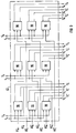
- FIG. 1 shows an inverter arrangement 2, which is fed on the input side with a DC voltage U GL .
- This inverter arrangement 2 consists of a parallel connection of a master inverter 4 and three slave inverters 6, 8 and 10.
- the outputs of each partial inverter 4 to 10 are provided with a choke 12.
- the phase conductors 14, 16 and 18 of the master inverter 4, the phase conductors 20, 22 and 24 of the slave inverter 6, the phase conductors 26, 28 and 30 of the slave inverter 8 and the phase conductors 32, 34 and 36 of the slave inverter 10 are electrically connected in parallel in phases.
- An induction machine 38 is connected to the conductors 14 to 36 connected in phase in parallel.
- a three-phase asynchronous machine is provided as the induction machine 38 and the partial inverters 4, 6, 8 and 10 are designed as six-pulse bridge circuits.
- This inverter arrangement 2 has an inverter control rate 40 which is supplied with a control voltage u St on the input side.
- This control voltage u St is generated in a control device, not shown, as a function of process data.
- the inverter control rate 40 generates six control signals S1, ..., S6 with known control methods, which are linked on the one hand with a downstream parallel switching module 42 and on the other hand directly with the control inputs 44 of the master inverter 4.
- a block diagram of the parallel switching module 42 is shown in more detail in FIG. 3.
- Control signals S are provided at each six outputs of this parallel switching module 42 ' 1 , ..., p ' 6 or S '' 1 , ..., p '' 6 or S "' 1 , ..., p "' 6 at.
- the outputs with the control signals S ' 1 , ..., p ' 6 are with the control inputs 46 of the slave inverter 6, the outputs with the control signals S '' 1 , ..., p '' 6 are with the control inputs 48 of the slave inverter 8 and the outputs with the control signals S "' 1 , ..., p "' 6 connected to the control inputs 49 of the slave inverter 10.
- the parallel switching module 42 is also electrically connected on the input side to current transformers 50 to 66. Through each converter 50, 56 and 62 or 52, 58 and 64 or 54, 60 and 66, a phase conductor 14 or 16 or 18 of the master inverter 4 and a phase conductor 20, 26 and 32 or 22, 28 and 34 or 24, 30 and 36 of the slave inverter 6 or 8 or 10 out.
- phase conductors of the master inverter 4 and a slave inverter 6 or 8 or 10 are each guided through the current transformers 50 to 66 in such a way that the phase currents I RM , I ' RS ; I SM , I ' SS ; I TM , I ' TS or I RM , I " RS ; I SM , I " SS ; I TM , I " TS or I RM , I "' RS ; I SM , I "' SS ; I TM , I "' TS flow in opposite directions.
- the control signals S are from the control signals S1, ..., S6 of the inverter headset 40 ' 1 , ..., p ' 6 , P '' 1 , ..., p '' 6 , P "' 1 , ..., p "' 6 generated.
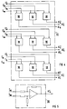
- the device according to FIG. 2 differs from the device according to FIG. 1 in that current detection devices 68 to 90 are used instead of the current transformers 50,... 66.
- the outputs of these current detection devices 68 to 90 are linked to a difference generator 92, which is shown in more detail in FIGS. 4 and 5.
- the outputs of this difference former 92 are connected to a parallel switching module 94, which is shown in more detail in FIG. 6.
- this parallel switching module 94 is also supplied with phase error voltage signals S UR , S US and S UT . Depending on its input signals, this parallel switching module 94 generates the control signals S.
- the parallel switching module 42 can also be combined with the difference former 92 and the current detection devices 68 to 90. Such a device is not shown in detail for reasons of clarity.
- FIG. 3 shows a block diagram of the parallel switching module 42 according to FIG. 1.
- This block diagram shows the internal structure of the parallel switching module 42.
- this parallel switching module 42 contains nine delay modules 96.
- FIG. 7 shows a block diagram of a delay module 96.
- Each delay module 96 has an actual phase current difference ⁇ I determined on the input side ' R , ..., ⁇ I ' T or ⁇ I '' R , ..., ⁇ I '' T or ⁇ I "' R , ..., ⁇ I "' T and two control signals S1, S4 and S2, S5 and S3, S6 supplied.
- the two control signals and the phase current actual value difference belong together in terms of phase.
- the generated control signals S ' 1 , ..., p ' 6 , P '' 1 , ..., p '' 6 , P "' 1 , ..., p “' 6 for the slave inverters 6 to 10 have been generated from the control signals S1, ..., S6 of the inverter tax rate 40 via a suitable change in the times for the switch-on and switch-off commands.
- the change in the time is determined in each case by a determined phase current actual value difference. 9 and 13 to 32, the relationship between control signals S1, ..., S6 and phase current actual value differences ⁇ I ' R , ..., ⁇ I ' T explained in more detail.
- FIG. 4 shows a block diagram of the difference generator 92 according to FIG. 2.
- this difference generator 92 contains nine cells 98, a circuit arrangement of a cell 98 being shown in more detail in FIG.
- each cell 98 contains an actual phase current value I RM or I RS or I RT of the master inverter 4 and an actual phase current value I ' RS or I ' SS or I ' TS of the slave inverter 6.
- I RS or I RS or I ' SS or I ' TS of the slave inverter 6.
- At the output of each cell 98 is the electronically determined phase current actual value difference ⁇ I ' R or ⁇ I ' S or ⁇ I ' T at.
- FIG. 5 A possible circuit arrangement of the cell 98 is shown in FIG. 5 and is described in more detail in the book "Semiconductor Circuit Technology", U. Tietze, Ch. Schenk, 1983, pages 300 to 304, in particular on page 301. Of course, there are also digital subtractors.
- FIG. 6 shows a block diagram of the parallel switching module 94 of FIG. 2.
- This block diagram differs from the block diagram according to FIG. 3 of the parallel switching module 42 according to FIG. 1 in that three delay modules 96 are added, each of which has a phase error voltage input at its inputs.
- Signal S UR or S US or S UT and two control signals S1, S4 or S2, S5 or S3, S6 of the control signals of the inverter headset 40 are pending.
- linearized control signals S are obtained ° 1 , P ° 4th or S ° 2nd , P ° 5 or S ° 3rd , P ° 6 for the master inverter 4.
- phase error voltage signals S UR , S US and S UT are determined by means of a circuit arrangement , not shown. These phase error voltage signals S UR , S US and S UT cause, like the phase current actual value differences ⁇ I ' R , ..., ⁇ I ' T or ⁇ I '' R , ..., ⁇ I '' T or ⁇ I "' R , ..., ⁇ I "' T a temporal change in the times for the switch-on and switch-off commands for the valves of the master inverter 4. This additional linearization of the control signals for the master inverter 4 ensures that the actual output voltage of the master inverter, because of the causes mentioned above , is also approximated for the fault voltage time areas of the voltage that the tax rate requires.
- FIG. 7 shows a block diagram of a delay module 96.
- This delay module 96 contains on the input side a first and a second switch-off delay module 100 and 102 and on the output side a first and a second switch-on delay module 104 and 106. It also contains the delay module 96 has an inverting matching amplifier 108 and an inverting amplifier 110.
- the delay modules 100 to 106 each have two inputs and one output and, as can be seen from FIG. 9, are constructed identically. A possible circuit arrangement of a delay module 100 is shown in more detail in FIG.
- the first switch-off delay module 100 and the first switch-on delay module 104 are electrically connected in series, just like the second switch-off delay module 102 and the second switch-on delay module 106.
- the output 112 and 114 of the first or second switch-off delay module 100 or 102 are linked to the control signal input 116 or 118 of the first or second switch-on delay module 104 or 106.
- the current input 120 or 122 of the first switch-off delay module 100 or of the second switch-on delay module 106 is connected to the output of the matching amplifier 108, at which the phase current actual value difference ⁇ I ' RN pending.
- the current input 124 or 126 of the second switch-off delay module 102 or of the first switch-on delay module 104 is linked to the output of the inverting amplifier 110, from which the phase current actual value difference ⁇ I ' RP pending.
- This actual value difference I ' RP is equal to the inverting actual value difference ⁇ I ' RN .
- the control signal input 128 of the first switch-off delay module 100 is the signal S1 of the inverter headset 40, the control signal S4 of the inverter headset 40 being supplied to the control signal input 130 of the second switch-off delay module 102.
- the control signal S is at the output 132 of the first switch-on delay module 104 ' 1 and at the output 134 of the second switch-on delay module 106 is the control signal S ' 4th removable for the slave inverter 6.
- the phase current actual value difference ⁇ I ' R whose polarity and amplitude suitably changes the times for the switching on and off commands of the valves of the slave inverter 6.
- the delay modules 100 to 106 are identical to FIG. 9 and FIG. 8 shows a circuit arrangement of the delay module 100.
- the signal input 128 is connected to a matching amplifier 136 with a downstream low-pass filter 138.
- the low-pass filter 138 is linked via an RCR element 140 to an inverting input of a comparator 142, the non-inverting input of which is connected to ground.
- the comparator 142 is connected to the output 112 of the delay module 100 via an RS flip-flop 144, which is constructed by means of a NAND gate.
- the current input 120 of this delay module 100 is also electrically conductively connected to the inverting input of the comparator 142 via a resistor.
- the signal input 128 of the delay module 100 is linked to an input of the RS flip-flop 144.
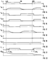
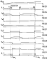
- the control signal S l , the filter output signal S lF , the comparator signal S lK and the complementary output signals S lFF and S lA are each shown in a diagram over time t in FIGS . 13 to 17.
- the corresponding signals for the downstream first switch-on delay module 104 are provided with a 'and are each shown in a diagram over time t in FIGS. 18 to 21.
- the waveforms of the second switch-off delay module 102 and the second switch-on delay module 106 are each shown in a diagram over time t in FIGS. 22 to 32.
- FIG. 9 shows, the actual phase current differences ⁇ I ' RN and ⁇ I ' RP , of the phase current actual value differences ⁇ I ' R suitably fed to the delay modules 100, ..., 106.
- the phase current actual value difference ⁇ I ' R I RM -I ' RS > 0 is.
- a bridge branch 146 of the master inverter 4 and a bridge branch 148 of the slave inverter 6 are each shown in detail in FIGS. 10 to 12. Both bridge branches 146 and 148 are electrically connected in parallel and are fed from a direct voltage source U GL .
- the bridge branch 146 and 148 contains two electrically connected valves Vl M and V4 M and Vl ' S and V4 ' S , which each have a free-wheeling diode Dl M and D4 M and Dl ' S and D4 ' S are connected in anti-parallel.
- the phase conductor 14 or 20 is connected, which are provided with the choke 12.
- Valve V4 M may only be activated after a storage time has elapsed, so that no bridge short-circuit occurs.
- a valve V4 becomes another delay time ⁇ te ⁇ ' S controlled ( Figures 24 and 32).
- the valves V4 M and V4 are switched off ' S nothing changes ( Figures 24 and 32).
- the delay time ⁇ te4 between switching on the valve V4 M and V4 ' S has become shorter ( Figures 13, 21, 24, 32). Is no actual phase current difference ⁇ I ' R have been determined, there is no longer a delay time ⁇ ta l and ⁇ te4.
- the control signal S l is fed via a low pass 138 to the inverting input of the comparator 142.
- the slope of the rising edge is changed.
Priority Applications (3)
| Application Number | Priority Date | Filing Date | Title |
|---|---|---|---|
| DE59009889T DE59009889D1 (de) | 1990-12-14 | 1990-12-14 | Verfahren und Vorrichtung zur Steuerung einer m-pulsigen Wechselrichteranordung, bestehend aus einem Master-Wechselrichter und wenigstens einem Slave-Wechselrichter. |
| EP90124288A EP0489971B1 (fr) | 1990-12-14 | 1990-12-14 | Méthode et dispositif pour la commande d'un système onduleur à m-impulsions, comprenant un onduleur "master" et au moins un onduleur "slave" |
| FI915609A FI915609A (fi) | 1990-12-14 | 1991-11-28 | Foerfarande och anordning foer styrning av en m-pulsvaexelriktaranordning som bestaor av en mastervaexelriktare och aotminstone en slavvaexelriktare. |
Applications Claiming Priority (1)
| Application Number | Priority Date | Filing Date | Title |
|---|---|---|---|
| EP90124288A EP0489971B1 (fr) | 1990-12-14 | 1990-12-14 | Méthode et dispositif pour la commande d'un système onduleur à m-impulsions, comprenant un onduleur "master" et au moins un onduleur "slave" |
Publications (2)
| Publication Number | Publication Date |
|---|---|
| EP0489971A1 true EP0489971A1 (fr) | 1992-06-17 |
| EP0489971B1 EP0489971B1 (fr) | 1995-11-15 |
Family
ID=8204844
Family Applications (1)
| Application Number | Title | Priority Date | Filing Date |
|---|---|---|---|
| EP90124288A Expired - Lifetime EP0489971B1 (fr) | 1990-12-14 | 1990-12-14 | Méthode et dispositif pour la commande d'un système onduleur à m-impulsions, comprenant un onduleur "master" et au moins un onduleur "slave" |
Country Status (3)
| Country | Link |
|---|---|
| EP (1) | EP0489971B1 (fr) |
| DE (1) | DE59009889D1 (fr) |
| FI (1) | FI915609A (fr) |
Cited By (10)
| Publication number | Priority date | Publication date | Assignee | Title |
|---|---|---|---|---|
| EP0600312A2 (fr) * | 1992-12-03 | 1994-06-08 | Inventio Ag | Méthode de contrôle pour onduleurs en parallèle au vu des extrema de courant |
| DE4323804A1 (de) * | 1993-07-15 | 1995-01-19 | Siemens Ag | Verfahren und Vorrichtung zur Steuerung einer m-pulsigen Wechselrichteranordnung, bestehend aus einem Master-Wechselrichter und wenigstens einem Slave-Wechselrichter |
| US5450309A (en) * | 1990-11-19 | 1995-09-12 | Inventio Ag | Method and device for switching inverters in parallel |
| EP0772288A2 (fr) * | 1995-10-31 | 1997-05-07 | Mitsubishi Denki Kabushiki Kaisha | Module semi-conducteur de puissance et module de puissance composé |
| EP0851567A2 (fr) * | 1996-12-24 | 1998-07-01 | Siemens Electric Limited | Système pour la connection en parallèle d'une pluralité de convertisseurs de puissance à source de tension |
| EP1047179A1 (fr) * | 1999-04-20 | 2000-10-25 | Sanyo Electric Co. Ltd | Méthode de commande d'un système d'alimentation à des onduleurs mis en parallèle et système de convertisseur |
| GB2359944A (en) * | 1999-12-16 | 2001-09-05 | Caterpillar Inc | Transmitting data in power systems |
| DE102005060354A1 (de) * | 2005-12-16 | 2007-06-21 | Siemens Ag | Modulares Umrichtersystem |
| WO2014113228A3 (fr) * | 2013-01-18 | 2015-01-29 | General Electric Company | Réglage d'équilibre de courant pour circuits à pont en parallèle non intercalés dans un convertisseur de puissance |
| DE102016215786A1 (de) | 2016-08-23 | 2018-03-01 | Robert Bosch Gmbh | Steuervorrichtung für eine elektrische Maschine, elektrisches Antriebssystem und Verfahren zur Ansteuerung einer elektrischen Maschine |
Citations (2)
| Publication number | Priority date | Publication date | Assignee | Title |
|---|---|---|---|---|
| GB1138357A (en) * | 1965-04-24 | 1969-01-01 | Int Standard Electric Corp | Arrangements for operating static inverters in parallel |
| DE3602496A1 (de) * | 1986-01-28 | 1987-07-30 | Klein Kg Elektro Geraete G | Verfahren zum parallelbetrieb von wechselrichtern und wechselrichteranordnung zur durchfuehrung des verfahrens |
-
1990
- 1990-12-14 EP EP90124288A patent/EP0489971B1/fr not_active Expired - Lifetime
- 1990-12-14 DE DE59009889T patent/DE59009889D1/de not_active Expired - Fee Related
-
1991
- 1991-11-28 FI FI915609A patent/FI915609A/fi not_active Application Discontinuation
Patent Citations (2)
| Publication number | Priority date | Publication date | Assignee | Title |
|---|---|---|---|---|
| GB1138357A (en) * | 1965-04-24 | 1969-01-01 | Int Standard Electric Corp | Arrangements for operating static inverters in parallel |
| DE3602496A1 (de) * | 1986-01-28 | 1987-07-30 | Klein Kg Elektro Geraete G | Verfahren zum parallelbetrieb von wechselrichtern und wechselrichteranordnung zur durchfuehrung des verfahrens |
Cited By (17)
| Publication number | Priority date | Publication date | Assignee | Title |
|---|---|---|---|---|
| US5450309A (en) * | 1990-11-19 | 1995-09-12 | Inventio Ag | Method and device for switching inverters in parallel |
| EP0600312A2 (fr) * | 1992-12-03 | 1994-06-08 | Inventio Ag | Méthode de contrôle pour onduleurs en parallèle au vu des extrema de courant |
| EP0600312A3 (fr) * | 1992-12-03 | 1994-11-30 | Inventio Ag | Méthode de contrÔle pour onduleurs en parallèle au vu des extrema de courant. |
| US5546298A (en) * | 1992-12-03 | 1996-08-13 | Inventio Ag | Method for the parallel connection of inverters by reference to extreme current values |
| DE4323804A1 (de) * | 1993-07-15 | 1995-01-19 | Siemens Ag | Verfahren und Vorrichtung zur Steuerung einer m-pulsigen Wechselrichteranordnung, bestehend aus einem Master-Wechselrichter und wenigstens einem Slave-Wechselrichter |
| WO1995002919A1 (fr) * | 1993-07-15 | 1995-01-26 | Siemens Aktiengesellschaft | Procede et dispositif pour la commande d'un dispositif onduleur a m impulsions comprenant un onduleur maitre et au moins un onduleur esclave |
| EP0772288A2 (fr) * | 1995-10-31 | 1997-05-07 | Mitsubishi Denki Kabushiki Kaisha | Module semi-conducteur de puissance et module de puissance composé |
| EP0772288A3 (fr) * | 1995-10-31 | 1999-02-17 | Mitsubishi Denki Kabushiki Kaisha | Module semi-conducteur de puissance et module de puissance composé |
| EP0851567A3 (fr) * | 1996-12-24 | 1999-01-13 | Siemens Electric Limited | Système pour la connection en parallèle d'une pluralité de convertisseurs de puissance à source de tension |
| EP0851567A2 (fr) * | 1996-12-24 | 1998-07-01 | Siemens Electric Limited | Système pour la connection en parallèle d'une pluralité de convertisseurs de puissance à source de tension |
| EP1047179A1 (fr) * | 1999-04-20 | 2000-10-25 | Sanyo Electric Co. Ltd | Méthode de commande d'un système d'alimentation à des onduleurs mis en parallèle et système de convertisseur |
| US6285572B1 (en) | 1999-04-20 | 2001-09-04 | Sanyo Electric Co., Ltd. | Method of operating a power supply system having parallel-connected inverters, and power converting system |
| GB2359944A (en) * | 1999-12-16 | 2001-09-05 | Caterpillar Inc | Transmitting data in power systems |
| DE102005060354A1 (de) * | 2005-12-16 | 2007-06-21 | Siemens Ag | Modulares Umrichtersystem |
| WO2014113228A3 (fr) * | 2013-01-18 | 2015-01-29 | General Electric Company | Réglage d'équilibre de courant pour circuits à pont en parallèle non intercalés dans un convertisseur de puissance |
| US9343991B2 (en) | 2013-01-18 | 2016-05-17 | General Electric Company | Current balance control for non-interleaved parallel bridge circuits in power converter |
| DE102016215786A1 (de) | 2016-08-23 | 2018-03-01 | Robert Bosch Gmbh | Steuervorrichtung für eine elektrische Maschine, elektrisches Antriebssystem und Verfahren zur Ansteuerung einer elektrischen Maschine |
Also Published As
| Publication number | Publication date |
|---|---|
| EP0489971B1 (fr) | 1995-11-15 |
| FI915609A (fi) | 1992-06-15 |
| FI915609A0 (fi) | 1991-11-28 |
| DE59009889D1 (de) | 1995-12-21 |
Similar Documents
| Publication | Publication Date | Title |
|---|---|---|
| EP0709000B1 (fr) | Procede et dispositif pour la commande d'un dispositif onduleur a m impulsions comprenant un onduleur maitre et au moins un onduleur esclave | |
| DE102015106069A1 (de) | Elektrische Motoransteuerungsvorrichtung | |
| DE2734467A1 (de) | Bremssteueranordnung fuer ein fahrmotorantriebssystem | |
| EP0023623A1 (fr) | Procédé pour détecter le courant de charge d'un régulateur inverseur à courant continu et circuit électrique pour la mise en oeuvre dudit procédé | |
| EP2608399B1 (fr) | Procédé de détection de défaut de terre pendant l'opération d'un convertisseur | |
| DE10260716A1 (de) | Mehrfach-PWM-Direktumrichter | |
| DE102016222361A1 (de) | Mehrphasen-elektromotorsteuerungsvorrichtung | |
| EP2494688B1 (fr) | Procédé pour faire fonctionner un circuit inverseur et dispositif pour mettre en oeliguvre le procédé | |
| EP0489971B1 (fr) | Méthode et dispositif pour la commande d'un système onduleur à m-impulsions, comprenant un onduleur "master" et au moins un onduleur "slave" | |
| EP2794334A1 (fr) | Dispositif de commande pour commutateur à semi-conducteur d'un onduleur et procédé permettant de commander un onduleur | |
| DE102018112147A1 (de) | Elektroantriebleistungswandler mit niedriger verzerrungstotzeiteinfügung | |
| DE102008023332A1 (de) | Dieselelektrisches Antriebssystem | |
| EP0082392A1 (fr) | Arrangement d'un circuit pour l'enregistrement de la polarité de courant d'une charge d'un hacheur réversible à courant continu | |
| DE3690376C2 (fr) | ||
| DE3521082A1 (de) | Wechselrichter und verfahren zu seinem betrieb | |
| DE102019204280A1 (de) | Steuergerät zur Bestimmung einer Totzeit für leistungselektronische Schalter | |
| DE3226001C2 (fr) | ||
| DE3703218C2 (fr) | ||
| EP0045951B1 (fr) | Procédé pour mettre en marche un convertisseur ayant un circuit intermédiaire à courant continu alimentant un moteur électrique synchrone | |
| DE3539027A1 (de) | Steuerverfahren und schaltungsanordnung fuer einen gleichrichter | |
| DE3714173C2 (fr) | ||
| EP0502226A1 (fr) | Procédé et dispositif pour simuler les courants dans une machine à champ tournant alimentée par onduleur | |
| DE3015108A1 (de) | Wechselrichtersystem und -verfahren sowie verfahren zum speisen eines wechselstrommotors | |
| EP3095178A1 (fr) | Convertisseur de puissance modulaire comprenant des sous-modules, lesquels fonctionnent en mode linéaire | |
| EP0288421B1 (fr) | Symétrisation des courants commutés par des semi-conducteurs commandés par la porte et disposés en parallèle |
Legal Events
| Date | Code | Title | Description |
|---|---|---|---|
| PUAI | Public reference made under article 153(3) epc to a published international application that has entered the european phase |
Free format text: ORIGINAL CODE: 0009012 |
|
| 17P | Request for examination filed |
Effective date: 19901214 |
|
| AK | Designated contracting states |
Kind code of ref document: A1 Designated state(s): AT BE CH DE DK ES FR GB GR IT LI LU NL SE |
|
| 17Q | First examination report despatched |
Effective date: 19930804 |
|
| GRAA | (expected) grant |
Free format text: ORIGINAL CODE: 0009210 |
|
| AK | Designated contracting states |
Kind code of ref document: B1 Designated state(s): CH DE FR GB IT LI SE |
|
| PG25 | Lapsed in a contracting state [announced via postgrant information from national office to epo] |
Ref country code: IT Free format text: LAPSE BECAUSE OF FAILURE TO SUBMIT A TRANSLATION OF THE DESCRIPTION OR TO PAY THE FEE WITHIN THE PRE;WARNING: LAPSES OF ITALIAN PATENTS WITH EFFECTIVE DATE BEFORE 2007 MAY HAVE OCCURRED AT ANY TIME BEFORE 2007. THE CORRECT EFFECTIVE DATE MAY BE DIFFERENT FROM THE ONE RECORDED.SCRIBED TIME-LIMIT Effective date: 19951115 |
|
| RIN1 | Information on inventor provided before grant (corrected) |
Inventor name: JEZ, JOZE |
|
| REF | Corresponds to: |
Ref document number: 59009889 Country of ref document: DE Date of ref document: 19951221 |
|
| PG25 | Lapsed in a contracting state [announced via postgrant information from national office to epo] |
Ref country code: LI Effective date: 19951231 Ref country code: CH Effective date: 19951231 |
|
| PG25 | Lapsed in a contracting state [announced via postgrant information from national office to epo] |
Ref country code: SE Effective date: 19960215 |
|
| ET | Fr: translation filed | ||
| GBT | Gb: translation of ep patent filed (gb section 77(6)(a)/1977) |
Effective date: 19960517 |
|
| REG | Reference to a national code |
Ref country code: CH Ref legal event code: PL |
|
| PLBE | No opposition filed within time limit |
Free format text: ORIGINAL CODE: 0009261 |
|
| STAA | Information on the status of an ep patent application or granted ep patent |
Free format text: STATUS: NO OPPOSITION FILED WITHIN TIME LIMIT |
|
| 26N | No opposition filed | ||
| PGFP | Annual fee paid to national office [announced via postgrant information from national office to epo] |
Ref country code: GB Payment date: 19971113 Year of fee payment: 8 |
|
| PGFP | Annual fee paid to national office [announced via postgrant information from national office to epo] |
Ref country code: FR Payment date: 19971219 Year of fee payment: 8 |
|
| PGFP | Annual fee paid to national office [announced via postgrant information from national office to epo] |
Ref country code: DE Payment date: 19980220 Year of fee payment: 8 |
|
| PG25 | Lapsed in a contracting state [announced via postgrant information from national office to epo] |
Ref country code: GB Effective date: 19981214 |
|
| GBPC | Gb: european patent ceased through non-payment of renewal fee |
Effective date: 19981214 |
|
| PG25 | Lapsed in a contracting state [announced via postgrant information from national office to epo] |
Ref country code: FR Free format text: LAPSE BECAUSE OF NON-PAYMENT OF DUE FEES Effective date: 19990831 |
|
| REG | Reference to a national code |
Ref country code: FR Ref legal event code: ST |
|
| PG25 | Lapsed in a contracting state [announced via postgrant information from national office to epo] |
Ref country code: DE Free format text: LAPSE BECAUSE OF NON-PAYMENT OF DUE FEES Effective date: 19991001 |