EP0488772A1 - Diodes électroluminescentes à semi-conducteur - Google Patents
Diodes électroluminescentes à semi-conducteur Download PDFInfo
- Publication number
- EP0488772A1 EP0488772A1 EP91311094A EP91311094A EP0488772A1 EP 0488772 A1 EP0488772 A1 EP 0488772A1 EP 91311094 A EP91311094 A EP 91311094A EP 91311094 A EP91311094 A EP 91311094A EP 0488772 A1 EP0488772 A1 EP 0488772A1
- Authority
- EP
- European Patent Office
- Prior art keywords
- array
- confinement layer
- layer
- light
- emitting
- Prior art date
- Legal status (The legal status is an assumption and is not a legal conclusion. Google has not performed a legal analysis and makes no representation as to the accuracy of the status listed.)
- Granted
Links
- 239000004065 semiconductor Substances 0.000 title claims abstract description 41
- 239000000758 substrate Substances 0.000 claims abstract description 58
- 230000005855 radiation Effects 0.000 claims abstract description 11
- 239000000463 material Substances 0.000 claims description 6
- 239000006117 anti-reflective coating Substances 0.000 claims description 4
- 230000003287 optical effect Effects 0.000 description 26
- 229910001218 Gallium arsenide Inorganic materials 0.000 description 21
- 238000003491 array Methods 0.000 description 14
- 239000012535 impurity Substances 0.000 description 11
- 238000000034 method Methods 0.000 description 11
- XUIMIQQOPSSXEZ-UHFFFAOYSA-N Silicon Chemical compound [Si] XUIMIQQOPSSXEZ-UHFFFAOYSA-N 0.000 description 8
- 229910052710 silicon Inorganic materials 0.000 description 8
- 239000010703 silicon Substances 0.000 description 8
- 238000002310 reflectometry Methods 0.000 description 7
- 229910016920 AlzGa1−z Inorganic materials 0.000 description 6
- 229910052785 arsenic Inorganic materials 0.000 description 6
- 239000011248 coating agent Substances 0.000 description 5
- 238000000576 coating method Methods 0.000 description 5
- 230000001427 coherent effect Effects 0.000 description 4
- 238000009792 diffusion process Methods 0.000 description 4
- 229910052751 metal Inorganic materials 0.000 description 4
- 239000002184 metal Substances 0.000 description 4
- 229910052581 Si3N4 Inorganic materials 0.000 description 3
- 239000000969 carrier Substances 0.000 description 3
- 230000017525 heat dissipation Effects 0.000 description 3
- 239000007943 implant Substances 0.000 description 3
- 238000002955 isolation Methods 0.000 description 3
- 229910000980 Aluminium gallium arsenide Inorganic materials 0.000 description 2
- KRHYYFGTRYWZRS-UHFFFAOYSA-N Fluorane Chemical compound F KRHYYFGTRYWZRS-UHFFFAOYSA-N 0.000 description 2
- 229910018885 Pt—Au Inorganic materials 0.000 description 2
- 238000003486 chemical etching Methods 0.000 description 2
- 239000002019 doping agent Substances 0.000 description 2
- 238000005516 engineering process Methods 0.000 description 2
- 229910052737 gold Inorganic materials 0.000 description 2
- 238000004519 manufacturing process Methods 0.000 description 2
- 238000001465 metallisation Methods 0.000 description 2
- 238000003892 spreading Methods 0.000 description 2
- 241001272720 Medialuna californiensis Species 0.000 description 1
- 229910052782 aluminium Inorganic materials 0.000 description 1
- 238000000137 annealing Methods 0.000 description 1
- 230000004888 barrier function Effects 0.000 description 1
- 230000015572 biosynthetic process Effects 0.000 description 1
- 238000005229 chemical vapour deposition Methods 0.000 description 1
- 238000004891 communication Methods 0.000 description 1
- 238000010276 construction Methods 0.000 description 1
- 238000007796 conventional method Methods 0.000 description 1
- 238000000151 deposition Methods 0.000 description 1
- 230000008021 deposition Effects 0.000 description 1
- 238000013461 design Methods 0.000 description 1
- 230000000694 effects Effects 0.000 description 1
- 230000002708 enhancing effect Effects 0.000 description 1
- 238000005530 etching Methods 0.000 description 1
- 230000008020 evaporation Effects 0.000 description 1
- 238000001704 evaporation Methods 0.000 description 1
- 239000000835 fiber Substances 0.000 description 1
- 229910052733 gallium Inorganic materials 0.000 description 1
- 239000011521 glass Substances 0.000 description 1
- 238000010438 heat treatment Methods 0.000 description 1
- 238000002513 implantation Methods 0.000 description 1
- 238000007648 laser printing Methods 0.000 description 1
- 238000001451 molecular beam epitaxy Methods 0.000 description 1
- TWNQGVIAIRXVLR-UHFFFAOYSA-N oxo(oxoalumanyloxy)alumane Chemical compound O=[Al]O[Al]=O TWNQGVIAIRXVLR-UHFFFAOYSA-N 0.000 description 1
- 238000002161 passivation Methods 0.000 description 1
- 238000001020 plasma etching Methods 0.000 description 1
- 238000007639 printing Methods 0.000 description 1
- 238000012545 processing Methods 0.000 description 1
- 238000007493 shaping process Methods 0.000 description 1
- 241000894007 species Species 0.000 description 1
- 238000000992 sputter etching Methods 0.000 description 1
- 239000010409 thin film Substances 0.000 description 1
- 229910052718 tin Inorganic materials 0.000 description 1
Images


Classifications
-
- B—PERFORMING OPERATIONS; TRANSPORTING
- B41—PRINTING; LINING MACHINES; TYPEWRITERS; STAMPS
- B41J—TYPEWRITERS; SELECTIVE PRINTING MECHANISMS, i.e. MECHANISMS PRINTING OTHERWISE THAN FROM A FORME; CORRECTION OF TYPOGRAPHICAL ERRORS
- B41J2/00—Typewriters or selective printing mechanisms characterised by the printing or marking process for which they are designed
- B41J2/435—Typewriters or selective printing mechanisms characterised by the printing or marking process for which they are designed characterised by selective application of radiation to a printing material or impression-transfer material
- B41J2/447—Typewriters or selective printing mechanisms characterised by the printing or marking process for which they are designed characterised by selective application of radiation to a printing material or impression-transfer material using arrays of radiation sources
- B41J2/45—Typewriters or selective printing mechanisms characterised by the printing or marking process for which they are designed characterised by selective application of radiation to a printing material or impression-transfer material using arrays of radiation sources using light-emitting diode [LED] or laser arrays
-
- H—ELECTRICITY
- H01—ELECTRIC ELEMENTS
- H01L—SEMICONDUCTOR DEVICES NOT COVERED BY CLASS H10
- H01L27/00—Devices consisting of a plurality of semiconductor or other solid-state components formed in or on a common substrate
- H01L27/15—Devices consisting of a plurality of semiconductor or other solid-state components formed in or on a common substrate including semiconductor components having potential barriers, specially adapted for light emission
- H01L27/153—Devices consisting of a plurality of semiconductor or other solid-state components formed in or on a common substrate including semiconductor components having potential barriers, specially adapted for light emission in a repetitive configuration, e.g. LED bars
-
- H—ELECTRICITY
- H01—ELECTRIC ELEMENTS
- H01S—DEVICES USING THE PROCESS OF LIGHT AMPLIFICATION BY STIMULATED EMISSION OF RADIATION [LASER] TO AMPLIFY OR GENERATE LIGHT; DEVICES USING STIMULATED EMISSION OF ELECTROMAGNETIC RADIATION IN WAVE RANGES OTHER THAN OPTICAL
- H01S5/00—Semiconductor lasers
- H01S5/40—Arrangement of two or more semiconductor lasers, not provided for in groups H01S5/02 - H01S5/30
- H01S5/42—Arrays of surface emitting lasers
- H01S5/423—Arrays of surface emitting lasers having a vertical cavity
-
- H—ELECTRICITY
- H01—ELECTRIC ELEMENTS
- H01S—DEVICES USING THE PROCESS OF LIGHT AMPLIFICATION BY STIMULATED EMISSION OF RADIATION [LASER] TO AMPLIFY OR GENERATE LIGHT; DEVICES USING STIMULATED EMISSION OF ELECTROMAGNETIC RADIATION IN WAVE RANGES OTHER THAN OPTICAL
- H01S2301/00—Functional characteristics
- H01S2301/18—Semiconductor lasers with special structural design for influencing the near- or far-field
-
- H—ELECTRICITY
- H01—ELECTRIC ELEMENTS
- H01S—DEVICES USING THE PROCESS OF LIGHT AMPLIFICATION BY STIMULATED EMISSION OF RADIATION [LASER] TO AMPLIFY OR GENERATE LIGHT; DEVICES USING STIMULATED EMISSION OF ELECTROMAGNETIC RADIATION IN WAVE RANGES OTHER THAN OPTICAL
- H01S5/00—Semiconductor lasers
- H01S5/02—Structural details or components not essential to laser action
- H01S5/026—Monolithically integrated components, e.g. waveguides, monitoring photo-detectors, drivers
-
- H—ELECTRICITY
- H01—ELECTRIC ELEMENTS
- H01S—DEVICES USING THE PROCESS OF LIGHT AMPLIFICATION BY STIMULATED EMISSION OF RADIATION [LASER] TO AMPLIFY OR GENERATE LIGHT; DEVICES USING STIMULATED EMISSION OF ELECTROMAGNETIC RADIATION IN WAVE RANGES OTHER THAN OPTICAL
- H01S5/00—Semiconductor lasers
- H01S5/10—Construction or shape of the optical resonator, e.g. extended or external cavity, coupled cavities, bent-guide, varying width, thickness or composition of the active region
- H01S5/18—Surface-emitting [SE] lasers, e.g. having both horizontal and vertical cavities
- H01S5/183—Surface-emitting [SE] lasers, e.g. having both horizontal and vertical cavities having only vertical cavities, e.g. vertical cavity surface-emitting lasers [VCSEL]
- H01S5/18308—Surface-emitting [SE] lasers, e.g. having both horizontal and vertical cavities having only vertical cavities, e.g. vertical cavity surface-emitting lasers [VCSEL] having a special structure for lateral current or light confinement
-
- H—ELECTRICITY
- H01—ELECTRIC ELEMENTS
- H01S—DEVICES USING THE PROCESS OF LIGHT AMPLIFICATION BY STIMULATED EMISSION OF RADIATION [LASER] TO AMPLIFY OR GENERATE LIGHT; DEVICES USING STIMULATED EMISSION OF ELECTROMAGNETIC RADIATION IN WAVE RANGES OTHER THAN OPTICAL
- H01S5/00—Semiconductor lasers
- H01S5/20—Structure or shape of the semiconductor body to guide the optical wave ; Confining structures perpendicular to the optical axis, e.g. index or gain guiding, stripe geometry, broad area lasers, gain tailoring, transverse or lateral reflectors, special cladding structures, MQW barrier reflection layers
- H01S5/2054—Methods of obtaining the confinement
- H01S5/2059—Methods of obtaining the confinement by means of particular conductivity zones, e.g. obtained by particle bombardment or diffusion
Definitions
- This invention relates to a semiconductor light-emitting diode structure and, more particularly, to a high-density surface-emitting semiconductor structure with independently-addressable individual light-emitting elements.
- the ability to fabricate closely-spaced, or high-density, independently-addressable laser and light-emitting diode (LED) sources is important for many applications, such as optical disk technology, laser printing and scanning, optical interconnection and fiber optic communications.
- semiconductor light-emitting diodes and semiconductor lasers are low-power output devices.
- Arrays of semiconductor light-emitting diodes or semiconductor lasers can be used to increase the power output and to simplify optical system design.
- arrays To provide and maintain good optical alignment of the light-emitting elements of the array with one another and to minimize the assembly involved, arrays have been fabricated so that the light-emitting elements are in a single semiconductor substrate.
- One problem with such arrays is maintaining the electrical and optical isolation between the individual light-emitting elements.
- Another problem is increasing the density of the light-emitting elements in the substrate by closely spacing the elements together while still maintaining the isolation, avoiding heat dissipation problems, and providing precise alignment of the elements.
- each individual light-emitting element in the array independently addressable. As the light-emitting elements are spaced closer together in higher densities, it is progressively more difficult to each element to emit light cause separately, individually and independently.
- Known laser and LED sources have been edge emitters, in which the radiation is emitted from the edge of a monolithic structure of semiconductor layers.
- An alternative construction is surface emitters, where the radiation is emitted from the surface of the monolithic structure of semiconductor layers.
- the light-emitting surface of a surface emitter is larger than that of an edge emitter.
- the power needed to cause emission of light is less for a surface emitter than an edge emitter.
- Surface-emitting LEDs are more efficient than edge emitting LEDs because they have that larger emitting area. Fabrication of surface emitting lasers can be less complex than fabrication of edge emitting lasers since the cleaving and mirror passivation needed for edge emitters are eliminated.
- the individual contacts that make the surface emitters of the array independently addressable are on the same side of the semiconductor as the light-emitting surface, the lateral spacing between the surface-emitting light sources is restricted, and consequently the density of the array is limited.
- the diameter of the contact will be larger than the diameter of the emitting surface.
- Annular contact shapes are also more difficult to contact while maintaining a clear aperture for the emitting surface.
- the contacts may require an auxiliary pad. Same surface contacts and emitting surfaces also may increase the amount of heat generated and may cause dissipation problems.
- the individual contacts that make the surface emitters of the array independently addressable should also be directly aligned with the light-emission optical cavity. Alignment is advantageous because it minimizes the electrical resistance, the current spreading to each emitter, and the size of the electrode. It also places the heat sink as close to the emitting area as possible. Minimizing current spreading helps electrically isolate the individual elements.
- a high-density surface emitting semiconductor LED array comprises a first confinement layer and a substrate of one conductivity type, an active layer, a second confinement layer and a contact layer of an opposing conductivity type. Disordered regions extend from the contact layer through to the first confinement layer defining light-emitting areas therebetween. The light-emitting areas can be laterally shaped for optimum use. Individual contacts on the second confinement layer aligned with each light-emitting area inject current through the light-emitting area to the contact on the substrate, causing emission of light from the active layer in the light-emitting area through the surface of the first confinement layer.
- the second confinement layer can be replaced with multiple layers making a highly reflective mirror known as a distributed Bragg reflector (DBR) to form an enhanced LED array.
- DBR distributed Bragg reflector
- Both confinement layers can be replaced with DBRs to form an optical cavity, instead of a light-emitting area, and a laser array rather than a LED array.
- either or both DBRs can be replaced with a confinement layer and a high reflectivity coating.
- a transparent refractive layer can be deposited between the substrate and the first confinement layer to diverge the emitted light.
- the output surface of the first confinement layer, the first DBR or the refractive layer can be etched to form a Fresnel lens for collimating or focussing the laser output.
- a micro lens array can be positioned adjacent to the surface emitting areas.
- the semiconductor laser/light-emitting diode arrays can also be formed into two-dimensional arrays.
- the semiconductor laser/light-emitting diode arrays can also be fabricated without the substrate.
- the bandgap of the semiconductor material of the active layer 16 is less than that of the first confinement layer 14 so that the first confinement layer is transparent to the light generated in the active layer.
- the first confinement layer also has a doping level as low as possible without introducing unnecessary resistance so that the first confinement layer is transparent to the light generated in the active layer.
- the substrate on the other hand, should be heavily doped to increase electrical conductivity.
- the first confinement layer 14 and the substrate 12 are both n-type conductivity, that side of the LED array is referred to as the n-side of the LED array.
- the second confinement layer 18 and the contact layer 20 are both p-type conductivity, that side of the LED array is referred to as the p-side of the LED array.
- the active layer may be nondoped, p-type doped or n-type doped; GaAs, Al z Ga 1-z As or (Al z Ga 1-z ) 0.5 ln 0.5 P; or a relatively thin conventional double heterostructure (DH) active layer; or a single quantum well, such as GaAs or Al z Ga 1-z As where z is very small and z ⁇ x and y; or a multiple quantum well superlattice, such as alternating layers of GaAs and Al z Ga 1-z As where z ⁇ x and y or alternating layers of Al w Ga 1-w As and Al B Ga 1-B As where w ⁇ B ⁇ x or y (w for well and B for barrier).
- any of the aforementioned active layers can be deposited between two semiconductor confinement layers of Al m Ga m-1 As and Al n Ga 1-n As, where m may or may not equal n, but with bandgaps intermediate the bandgaps of the active layer and the first and second confinement layers, in a separate confinement structure.
- the epitaxial growth of LED array 10 may be carried out by molecular beam epitaxy (MBE) or metallo-organic chemical vapor deposition (MOCVD).
- the substrate 12 may be about 100 ⁇ m thick.
- Confinement layers 14 and 18 may have a thickness in the range of 0. 1 to 1 ⁇ m.
- Active layer 16 may be a thin conventional layer, having a thickness of 50 nm to 2 ⁇ m or may be comprised of a superlattice structure of quantum wells which may be 3 to 50 nm thick.
- the contact layer is typically 0. 1 to 0.2 ⁇ m thick.
- a Si3N4 mask is formed on the top surface 22 of the contact layer 20 with openings exposing regions of the semiconductor structure to impurity-induced disordering.
- the mask protects the unexposed regions which will form and shape the light-emitting areas, which can be circular, elliptical, square, rectangular, trapezoidal, triangular or of any desired shape or size.
- the light-emitting areas are established by first selectively diffusing a high concentration n-impurity dopant, such as silicon, into the regions of the semiconductor structure exposed through the mask.
- n-impurity dopant such as silicon
- Other n-impurity dopant elements would include Ge and Sn.
- a silicon layer is deposited in the opening in the Si3N4 mask and then capped with an additional layer of Si3N4.
- the diffusion of silicon is accomplished at a temperature of approximately 800° C and is maintained for a sufficiently long period, e.g. seven to eight hours, for the silicon to penetrate the contact layer 20, the second confinement layer 18 and the active layer 16, and partially penetrate the first confinement layer 14.
- the diffusion of silicon through and into the active layer 16, the contact layer 20 and the confinement layers 14 and 18 causes an intermixing of Ga and Al in the active layer 16, the contact layer 20 and the confinement layers 14 and 18, thereby forming a n-impurity induced disordered region 24.
- electrically-insulating regions 26 are formed in the disordered regions 24 by proton implantation through the top surface 22 to provide a level of electrical isolation of the light-emitting areas, which allows independent addressability of each individual light-emitting area.
- the light-emitting areas 28 consisting of the non-disordered sections of the second confinement layer 18, the active layer 16 and the first confinement layer 14.
- the disordered regions optically and electrically, isolate and separate the light-emitting areas.
- the light-emitting areas are shaped by the confinement layers in the vertical direction and the shape of the disordered regions in the horizontal direction.
- metal contacts 30 of Cr-Au or Ti-Pt-Au are employed to form metal contacts 30 of Cr-Au or Ti-Pt-Au on the top surface 22 of the non-disordered contact layer 20 aligned with each optical cavity 28.
- Each contact 30 contacts an optical cavity.
- the contacts 30 are referred to as p-contacts, since they are on the p-side of the LED array.
- the contacts are typically circular or annular in shape for ease in forming high density arrays, although the contacts may also be elliptical, half-moon or other shapes.
- the individual contact can be equal in size or smaller than the active layer in the aligned light-emitter area, and can be shaped to match the active layer or the light emitter area.
- the contact is shaped by shaping the hole in a metallization mask.
- the shape of the contact is important so that the contact has the largest area possible, for reducing electrical resistance without limiting the density of the emitters, and to match the bonding pad for effective heat dissipation.
- the non-disordered contact layer 20 beneath each contact 30 provides low contact resistance to the other semiconductor layers, and reduces contact heating.
- the bottom surface 32 of the substrate 12 is also metallized with Au/Ge to form a substrate contact 34.
- the substrate contact is referenced to ground and referred to as the n-contact, since it is on the n-side of the LED array.
- the current is injected between the p-contact 30 and the n-contact 34 to forward-bias the p-n junction of p-confinement layer 18 and n-confinement layer 14 to cause the active layer 16 to emit light 36 from the light-emitting area 28.
- the current is injected substantially parallel to the light-emitting area, through the p-contact 30, the p-contact layer 20, the p-confinement layer 18, the active layer 16 of the individual light-emitting area, and then spreads in the n-confinement layer 14 into the substrate 12 and out the n-contact 34.
- each light-emitting area or LED element contains a p-n junction that is separately biased through its p-contact from all the others. Since each p-contact is positively biased with respect to ground, current flows only from each p-contact to ground. The electrically isolating regions and the disordered regions prevent any single p-contact from causing adjacent light-emitting areas to emit light. Flow between different p-contacts does not occur, because any small potential difference between the addressed p-contact and a neighboring p-contact corresponds to a reverse voltage on the neighboring p-contact.
- the light 36 is emitted through the emitter surface area 38, substantially perpendicular to the bottom surface 32 of the substrate 12 and aligned with the p-contact 30 and the light-emitting area 28, hence LED array 10 is a surface emitting LED.
- the p-contact 30 aligned with the light-emitting area 28 prevents light from being emitted through the p-side of the LED array.
- the shape of the emitter surface area, and therefore the cross-sectional shape of the resulting beam of emitted radiation is determined by the shape of the light-emitting areas, which can be circular, elliptical, square, rectangular, trapezoidal, triangular or any desired shape or size.
- the emitted light itself can be either continuous wave or pulse.
- the LED array 10 has an operating current of about 10 mA with an output power of about 30 ⁇ W per individual light-emitting element.
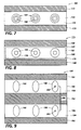
- Figure 2 is the bottom view of the LED array 10 of Figure 1, showing the bottom surface 32 of the substrate with the stripe n-contacts 34 and the array of circular emitter surface areas 38 of the light-emitting areas where the light is emitted through the surface between the n-contacts.
- the thickness of the substrate 12 may impede emission of the light from the active layer of the LED array.
- the active layer can be made of semiconductor material with a bandgap less than the bandgap of the substrate.
- the substrate can be removed.
- a trough 40 or stripe is etched in the surface 32 of the substrate 12, by standard chemical etching or other techniques, to expose the surface 42 of the first confinement layer 14 to expose the emitter surface areas 38 of the LED optical cavities 28 therebeneath to facilitate light emission.
- the exposed surface of the first confinement layer may also be coated with an anti-reflective coating to facilitate light emission.
- the processing of the LED array 10 is done from both the p-side and the n-side of the LED array.
- the active layer is shallower in the LED array and closer to the light-emitting surface. Similarly, the light emitted from the active layer does not pass through a heavily-doped contact layer, unlike when the individual contacts and the light-emitting surface areas are on the same side of the light-emitting semiconductor.
- the diameters of the emitter surface areas 38 are typically 2 ⁇ m or less.
- the spacing 44 from the center 46 of one individual LED element to the center 46 of the next LED element, as measured from the emitter surface areas 38, is 3 ⁇ m or less, which provides for a high density of LEDs in the array.
- the impurity-induced disordering provides accurate and closer center-to-center spacing of the individual LED elements.
- the lateral spacing of the light-emitting elements is slightly closer.
- the light emitter geometry can be staggered or offset if the p-contacts and the light-emitter areas are also staggered, rather than the straight line of p-contacts and LED emitter surface areas shown in Figure 2.
- a staggered or offset geometry provides a higher density of LED elements.
- enhanced LED array 48 is of identical structure to the LED array 10 of Figure 1, except that the p-confinement layer 18 of Figure 1 has been replaced by a distributed Bragg reflector (DBR) 50.
- the LED array 48 comprises a substrate 52 of n-GaAs upon which is epitaxially deposited a confinement layer 54 of n-Al x Ga 1-x As; an active layer 56 of nondoped GaAs for providing light wave generation and propagation, a p-DBR 50 of alternating layers of p-Al y Ga 1-y As and p-Al z Ga 1-z As where z ⁇ y, and a contact layer 58 of p-GaAs.
- DBR distributed Bragg reflector
- N-impurity-induced disordered regions 60 are formed in the enhanced LED array 48 extending through portions of the contact layer 58, the p-DBR 50, the active layer 56 and the n-confinement layer 54. Electrical isolating regions 62 are formed on the top surface of the disordered regions.
- the enhanced LED light-emitting areas 64 consisting of the non-disordered sections of the p-DBR 50, the active layer 56 and the n-confinement layer 54.
- the p-DBR is constructed to have a reflectivity as close to unity as possible.
- P-contacts 66 are formed on the p-contact layer 58, aligned with each enhanced LED light-emitting area 64 and a n-contact 68 is formed on the substrate 52, except in a trough formed in the substrate (not shown).
- the light 70 is emitted through the emitter surface area 72 on the bottom surface of the n-confinement layer, substantially perpendicular to the bottom surface 74 of the substrate 52.
- the p-DBR reflects the light being emitted by the optical cavity toward the p-side of the LED array back through the surface area on the n-side of the LED array, thus enhancing the amount of light emission of the LED array.
- the exposed surface of the confinement layer and the emitter surface area in the trough may also be coated with an anti-reflective coating to facilitate light emission.
- the enhanced LED array 48 has an operating current of about 10 mA with an output power of about 60 ⁇ W.
- the active layer 56 can be in a separate confinement structure to keep the carriers away from the DBR.
- the p-confinement layer 18 of Figure 1 may be coated with a highly-reflective metal which serves as an electrically-conductive, optical reflector to form an enhanced LED array.
- laser array 76 is of identical structure to the array 48 of Figure 3, except that the n-confinement layer 54 of Figure 3 has been replaced by a DBR 78 and that active layer 56 of Figure 3 has been replaced by active layer 80 which provides lightwave generation and propagation under lasing conditions.
- the laser array 76 comprises a substrate 82 of n-GaAs upon which is epitaxially deposited a n-DBR 78 of alternating layers of n-Al x Ga 1-x As and n-Al y Ga 1-y As where x ⁇ y, an active layer 80 of nondoped GaAs for providing light wave generation and propagation under lasing conditions, a p-DBR 84 of alternating layers of p-Al A Ga 1-A As and p-Al B Ga 1-B As where A ⁇ B, and a contact layer 86 of p-GaAs.
- N-impurity induced disordered regions 88 are formed in the laser array 76 extending through portions of the contact layer 86, the p-DBR 84, the active layer 80 and the n-DBR 78. Electrical isolating regions 90 are formed on the top surface of the disordered regions.
- the laser optical cavity regions 92 consisting of the non-disordered sections of the p-DBR 84, the active layer 80 and the n-DBR 78.
- the p-DBR is constructed to have a reflectivity as close to unity as possible, while the n-DBR is constructed with a reflectivity close to unity but less than that of the p-DBR.
- P-contacts 94 are formed on the p-DBR 84 aligned with each laser optical cavity regions 92, and a n-contact 96 is formed on the substrate 82 except in a trough formed in the substrate (not shown).
- the light 98 is emitted through the emitter surface area 100 on the bottom surface of the n-DBR in the trough (not shown) in the substrate, substantially perpendicular to the bottom surface 102 of the substrate 82.
- An anti-reflective coating is not required to coat the trough. Since the light is from a laser optical cavity, it is, of course, coherent and can be either continuous wave or pulse.
- the laser array 76 has a threshold current of 1 to 5 mA and an operating current of about 10 mA with an output power of about 1 to 3 mW. Threshold currents of less than 1 mA are also possible for the laser array.
- the active layer 80 can be in a separate confinement structure to keep the carriers away from the DBR.
- the p-confinement layer 18 of Figure 1 which was replaced by a distributed Bragg reflector (DBR) 84 in Figure 4, may be coated with a highly-reflective metal which serves as an electrically-conductive, optical reflector to form a laser array.
- DBR distributed Bragg reflector
- the laser array 104 is of identical structure to the laser array 76 of Figure 4, except that the n-DBR 74 has been replaced with a n-confinement layer 106 and a high reflectivity coating 108.
- the laser array 104 comprises a substrate 110 of n-GaAs, a n-confinement layer 106 of n-Al x Ga 1-x As, an active layer 112 of nondoped GaAs, a p-DBR 114 of alternating layers of p-Al y Ga 1-y As and p-Al z Ga 1-z As where z ⁇ y, a contact layer 116, n-impurity induced disordered regions 118, electrical isolating regions 120, laser optical cavity 122, p-contacts 124, and stripe n-contact 126 formed on the substrate 110, along with a trough in the substrate (not shown).
- a high reflectivity coating 108 is deposited by evaporation on the exposed surface of the n-confinement layer 106.
- the coating covers the surface emitter areas 128 and forms one end of the laser optical cavity 122.
- the high reflectivity coating is typically a multilayer stack of materials such as silicon and aluminum oxide, as is known.
- the active layer 112 can be in a separte confinement structure to keep the carriers away from the DBR.
- the p-confinement layer 18 of Figure 1 which was replaced by a distributed Bragg reflector (DBR) 114 in Figure 5, may instead be coated with a highly-reflective metal to serve as an electrically-conductive optical reflector.
- DBR distributed Bragg reflector
- the laser array 130 is of identical structure to the laser array 72 of Figure 4, except that a refractive layer 132 is deposited between the substrate 134 and the n-DBR 136.
- the laser array 130 comprises a substrate 134 of n-GaAs upon which is deposited a refractive layer 132 of Al v Ga 1-v As, a n-DBR 136 of alternating layers of n-Al x Ga 1-x As and n-Al y Ga 1-y As where x ⁇ y, an active layer 138 of nondoped GaAs, a p-DBR 140 of alternating layers of p-Al x Ga 1-x As and p-Al y Ga 1-y As where x ⁇ y, and a contact layer 142 of p-GaAs.
- the laser array further comprises n-impurity induced disordered regions 144 and electrical isolating regions 146.
- the laser optical cavity 148 consists of the non-disordered sections of the p-DBR 140, active layer 138 and n-DBR 136.
- the emitter surface areas 150 are the interface surface 152 between the n-DB R 136 and the refractive layer 132.
- P-contacts 154 are formed on the p-DBR 140, and a stripe n-contact 156 is formed on the substrate 134.
- a trough (not shown) is etched in the substrate 134 to expose the surface 158 of the refractive layer 132.
- the refractive layer is transparent to light emitted from the laser optical cavity through the emitter surface areas, but the refractive layer does diverge the light 160 emitted from the laser array, increasing the output spot size.
- the refractive layer should be thick enough to give the appropriate expansion of the spot size. A 5 to 10 ⁇ m thick refractive layer, for example, should double the size of the spot.
- Increasing the thickness of the refractive layer 132 increases the refractive power, diverges the angle of the emitted light further and increases the output spot size. Selection of an appropriate thickness for the refractive layer will result in partially-overlapping output spots of emitted light between the adjacent laser optical cavities of the adjacent laser elements. Fabricating the surface emitter area in an elliptical shape, for example, will further facilitate overlapping the diverging emitted light in the short axis direction of the ellipse. Overlapping in the long axis direction is pertinent to printing, where controlled overlap from line to line may be desirable.
- the refractive layer is that no phase coherence is introduced between adjacent laser emitters. Consequently, the overlapping beams can be used optically without any optical interference effects.
- the refractive layer of AlGaAs can still be used to diverge the light emitted from the array, although it would not be as effective as with light emitted from a laser, since the radiation pattern from an LED is lambertian.
- a laser array 162 is fabricated in the identical fashion to laser array 76 of Figure 4, except that fresnel lenses 164 are formed on the exposed n-DBR 166 over the emitter surface areas 168.
- the laser array 162 has stripe n-contacts 170 alternating with troughs 172 of the exposed surfaces 166 of the n-DBR with its emitter surface areas 168.
- a fresnel lens 164 is formed for each individual laser element by etching, by ion milling, reactive ion etching or other means.
- Each lens can be shaped to magnify the spot size of the emitted light, change the direction of the emitted light or otherwise alter the emitted light optically.
- the lateral shape of the lens can be formed to match the transverse shape of the optical cavity.
- the fresnel lenses can still be used to collimate, diverge, focus or otherwise modify the light emitted from the array by forming the lenses in the n-confinement layer over the emitter surface areas, although it would not be as effective as with light emitted from a laser since the radiation pattern from a LED is lambertian.
- Fresnel lenses can also be formed in the refractive layer of Figure 6 over the emitter surface areas.
- a laser array 174 is fabricated in identical fashion to laser array 76 of Figure 4 except that an array 176 of micro lenses 178 is positioned flush in the trough 180 of the exposed surface 182 of the n-DBR 184. Each micro lens 178 is aligned with an emitter surface area 186.
- the laser array 174 has stripe n-contacts 188 alternating with the troughs 180 and the micro lens array 176 positioned within the trough.
- Each micro lens 178 in the array is formed for each individual laser element by known means.
- Each micro lens can be shaped to magnify the spot size of the emitted light, change the direction of the emitted light or otherwise modify the emitted light optically.
- the lateral shape of the micro lens can be formed to match the transverse shape of the optical cavity.
- the micro lens array can be positioned adjacent to the emitter surface areas of the LED array to magnify the size and spacing of the light-emitting areas.
- a 3 ⁇ m spaced array over a 30 mm distance with an optical magnification of 7 will result in 48 spots per mm over a pagewidth of 212 mm.
- a 4.5 ⁇ m spacing of an array will yield 32 spots per mm for a pagewidth.
- the micro lens array can still be used to collimate, diverge, focus or otherwise modify the light emitted from the LED or enhanced LED array by positioning the micro lens array over the emitter surface areas.
- a micro lens array can also be used with the refractive layer of Figure 6 over the emitter surface areas.
- the driver circuitry for the p-contacts and the necessary bonding pads can be fabricated on a silicon chip (not shown) placed flush against the top surface of the LED or laser array.
- the silicon chip need not be optically transparent since the light emission will be from the other surface of the LED or laser array.
- electronic driver circuitry can be fabricated on the semiconductor LED or laser array or separate and adjacent to the array or on or in the substrate of the semiconductor array. Since the p-contact is directly below the active region, and the light is emitted from the surface of the n-side of the array, the full cross-sectional area of the array is used for heat dissipation.
- a two-dimensional array 190 is fabricated in the identical fashion to laser array 76 of Figure 4 except that linear arrays are formed adjacent to each other.
- the two-dimensional array 190 has stripe n-contacts 192 alternating with troughs 194 of the exposed surfaces 196 of n-DBRs with its elliptical emitter surface areas 198.
- the spacing 200 between the center 202 of one individual laser element in one linear array row to the center 202 of one corresponding individual laser element in the next linear array row, as measured from the emitter surface areas 198, is typically 9 to 18 ⁇ m which provides for a high density of laser elements in the two-dimensional array.
- Two-dimensional arrays of surface emitters can be used to expose several lines simultaneously or sequential interlacing of the printed lines. In combination with a refractive layer, two-dimensional arrays can provide optimum overlap of scanning lines.
- the two-dimensional array is also not restricted to linear rows and columns of surface emitters but the surface emitter layout can be staggered or offset.
- the two-dimensional laser array is by way of illustration.
- the LED and enhanced LED arrays can also be fabricated into a two-dimensional array.
- Refractive layers, fresnel lens and micro lens arrays, as previously, discussed can also be used with a two-dimensional array.
- the above embodiments of this invention have all been fabricated with a substrate which, to facilitate light emission, has a trough etched in the substrate to the confinement layer or DBR therebeneath to expose the surface emitters.
- the arrays can be fabricated without the substrate and resulting etched trough through the epitaxial liftoff method as described by Yablonitch et al., (" Double Heterostructure GaAs/AlGaAs Thin Film Diode Lasers on Glass Substrates ", IEEE Photonics Technology Letters , Vol. 1, No.2, pp.41-42February 1989).
- the epitaxial liftoff method as shown in Figure 10 provides for a selective release layer 204 of n-AlAs to be deposited on a substrate 206 of GaAs.
- the release layer is approximately 50 nm thick.
- a LED array 208 is then fabricated on the selective release layer 204.
- a first confinement layer 210 of n-Al x Ga 1-x As is epitaxially deposited on the release layer, followed by the deposition of an active layer 212 of nondoped GaAs for providing light wave generation and propagation, a second confinement layer 214 of p-Al y Ga 1-y As where x may or may not equal y, and a contact layer 216 of p-GaAs.
- N-disordered regions 218, electrically insulating regions 220 and p-contacts 222 are formed on the LED array 208 as taught previously in this application with regard to the LED array 10 of Figure 1.
- the release layer 204 is then removed by dilute hydrofluoric acid, allowing the LED array 208 to be removed from the substrate 206.
- the LED or laser array is then attached to or made part of the necessary driver circuits, as discussed above. Alternatively, the array can be attached to a patterned carrier that enables separate addressing of each element.
- the stripe n-contact (not shown) of Cr-Au or Ti-Pt-Au is then formed by metallization on the surface of the first confinement layer 210. Since there is no substrate, there is no need for a trough to expose the surface emitter on the surface of the first confinement layer, as the surface emitter is already exposed between the n-contacts.
- the LED array 208 was fabricated by the epitaxial liftoff method.
- the enhanced LED and laser arrays can also be fabricated by the same method without a substrate.
- a refractive layer can be epitaxially deposited on the selective release layer, followed by a first confinement layer or a distributed Bragg reflector.
- fresnel lenses can be fabricated over the surface emitting areas, once the LED or laser array has been removed from the substrate by the epitaxial liftoff method.
- a micro lens array can be positioned flush with the surface emitting areas or positioned adjacent to the surface emitting areas, once the LED or laser array has been removed from the substrate by the epitaxial liftoff method.
- a two-dimensional array of LED/laser elements can be fabricated by the same method as taught in Figure 10, without the semiconductor element of a substrate and the resulting trough etched in the substrate to the confinement layer or DBR therebeneath.
Landscapes
- Physics & Mathematics (AREA)
- Engineering & Computer Science (AREA)
- Condensed Matter Physics & Semiconductors (AREA)
- General Physics & Mathematics (AREA)
- Power Engineering (AREA)
- Optics & Photonics (AREA)
- Microelectronics & Electronic Packaging (AREA)
- Computer Hardware Design (AREA)
- Health & Medical Sciences (AREA)
- General Health & Medical Sciences (AREA)
- Toxicology (AREA)
- Electromagnetism (AREA)
- Semiconductor Lasers (AREA)
- Led Devices (AREA)
Applications Claiming Priority (2)
| Application Number | Priority Date | Filing Date | Title |
|---|---|---|---|
| US07/620,229 US5216263A (en) | 1990-11-29 | 1990-11-29 | High density, independently addressable, surface emitting semiconductor laser-light emitting diode arrays |
| US620229 | 1996-03-22 |
Publications (2)
| Publication Number | Publication Date |
|---|---|
| EP0488772A1 true EP0488772A1 (fr) | 1992-06-03 |
| EP0488772B1 EP0488772B1 (fr) | 1997-09-17 |
Family
ID=24485100
Family Applications (1)
| Application Number | Title | Priority Date | Filing Date |
|---|---|---|---|
| EP91311094A Expired - Lifetime EP0488772B1 (fr) | 1990-11-29 | 1991-11-29 | Diodes électroluminescentes à semi-conducteur |
Country Status (5)
| Country | Link |
|---|---|
| US (2) | US5216263A (fr) |
| EP (1) | EP0488772B1 (fr) |
| JP (1) | JPH04234190A (fr) |
| CA (1) | CA2051223C (fr) |
| DE (1) | DE69127677T2 (fr) |
Cited By (17)
| Publication number | Priority date | Publication date | Assignee | Title |
|---|---|---|---|---|
| EP0641116A1 (fr) * | 1993-08-23 | 1995-03-01 | Xerox Corporation | Diode laser multipoint avec microoptique pour systèmes de balayage à plusieurs faisceaux |
| FR2730035A1 (fr) * | 1995-01-30 | 1996-08-02 | Valeo Vision | Projecteur infrarouge pour systeme d'aide a la vision pour vehicule automobile et systeme d'aide a la vision le comportant |
| EP2280430A3 (fr) * | 2005-03-11 | 2012-08-29 | Seoul Semiconductor Co., Ltd. | Boîtier de diodes électroluminescentes à matrice de cellules photoémettrices montées en série |
| WO2017222618A1 (fr) * | 2016-06-23 | 2017-12-28 | Apple Inc. | Réseau vcsel á émission haute et diffuseur intégré |
| EP3382828A1 (fr) * | 2017-03-31 | 2018-10-03 | Koninklijke Philips N.V. | Agencement de laser à sécurité intrinsèque comprenant un laser à cavité verticale émettant en surface |
| CN108923261A (zh) * | 2018-10-24 | 2018-11-30 | 常州纵慧芯光半导体科技有限公司 | 垂直腔面发射激光器的像素结构及其制作方法 |
| EP3509170A1 (fr) * | 2018-01-05 | 2019-07-10 | Koninklijke Philips N.V. | Agencement de laser économe en énergie |
| WO2020104495A1 (fr) * | 2018-11-22 | 2020-05-28 | Aledia | Diode électroluminescente et procédé de fabrication d'une diode électroluminescente |
| WO2021052635A3 (fr) * | 2019-09-20 | 2021-05-06 | Osram Opto Semiconductors Gmbh | Composant optoélectronique, structure semi-conductrice et procédé |
| US11156759B2 (en) | 2019-01-29 | 2021-10-26 | Osram Opto Semiconductors Gmbh | μ-LED, μ-LED device, display and method for the same |
| US11178392B2 (en) | 2018-09-12 | 2021-11-16 | Apple Inc. | Integrated optical emitters and applications thereof |
| US11271143B2 (en) | 2019-01-29 | 2022-03-08 | Osram Opto Semiconductors Gmbh | μ-LED, μ-LED device, display and method for the same |
| US11302248B2 (en) | 2019-01-29 | 2022-04-12 | Osram Opto Semiconductors Gmbh | U-led, u-led device, display and method for the same |
| US11469573B2 (en) | 2019-02-04 | 2022-10-11 | Apple Inc. | Vertical emitters with integral microlenses |
| US11538852B2 (en) | 2019-04-23 | 2022-12-27 | Osram Opto Semiconductors Gmbh | μ-LED, μ-LED device, display and method for the same |
| US11610868B2 (en) | 2019-01-29 | 2023-03-21 | Osram Opto Semiconductors Gmbh | μ-LED, μ-LED device, display and method for the same |
| US11994694B2 (en) | 2021-10-24 | 2024-05-28 | Apple Inc. | Microlens array with tailored sag profile |
Families Citing this family (112)
| Publication number | Priority date | Publication date | Assignee | Title |
|---|---|---|---|---|
| US5216263A (en) * | 1990-11-29 | 1993-06-01 | Xerox Corporation | High density, independently addressable, surface emitting semiconductor laser-light emitting diode arrays |
| US5745153A (en) * | 1992-12-07 | 1998-04-28 | Eastman Kodak Company | Optical means for using diode laser arrays in laser multibeam printers and recorders |
| US5606572A (en) * | 1994-03-24 | 1997-02-25 | Vixel Corporation | Integration of laser with photodiode for feedback control |
| US5453386A (en) * | 1994-05-09 | 1995-09-26 | Motorola, Inc. | Method of fabrication of implanted LED array |
| US5729563A (en) * | 1994-07-07 | 1998-03-17 | Hewlett-Packard Company | Method and apparatus for optically and thermally isolating surface emitting laser diodes |
| US5610095A (en) * | 1994-08-31 | 1997-03-11 | Lucent Technologies Inc. | Monolithically integrated circuits having dielectrically isolated, electrically controlled optical devices and process for fabricating the same |
| US5811839A (en) | 1994-09-01 | 1998-09-22 | Mitsubishi Chemical Corporation | Semiconductor light-emitting devices |
| JP3773282B2 (ja) * | 1995-03-27 | 2006-05-10 | 豊田合成株式会社 | 窒化ガリウム系化合物半導体の電極形成方法 |
| US5978401A (en) * | 1995-10-25 | 1999-11-02 | Honeywell Inc. | Monolithic vertical cavity surface emitting laser and resonant cavity photodetector transceiver |
| SE509809C2 (sv) * | 1995-11-03 | 1999-03-08 | Mitel Semiconductor Ab | Lysdiod med uppdelat ljusemitterande område |
| US5956070A (en) | 1995-12-22 | 1999-09-21 | Xerox Corporation | Color xerographic printer with multiple linear arrays of surface emitting lasers with dissimilar polarization states and dissimilar wavelengths |
| JPH09185207A (ja) | 1995-12-22 | 1997-07-15 | Xerox Corp | 同一波長を有する表面放射レーザーの多数のリニアアレイを有するカラー電子写真式プリンタ |
| US5745517A (en) * | 1995-12-29 | 1998-04-28 | Xerox Corporation | Alternative doping for AlGaInP laser diodes fabricated by impurity-induced layer disordering (IILD) |
| US5898211A (en) * | 1996-04-30 | 1999-04-27 | Cutting Edge Optronics, Inc. | Laser diode package with heat sink |
| US5838715A (en) * | 1996-06-20 | 1998-11-17 | Hewlett-Packard Company | High intensity single-mode VCSELs |
| US5914760A (en) * | 1996-06-21 | 1999-06-22 | Casio Computer Co., Ltd. | Surface light source device and liquid crystal display device using the same |
| US5734672A (en) * | 1996-08-06 | 1998-03-31 | Cutting Edge Optronics, Inc. | Smart laser diode array assembly and operating method using same |
| US5835517A (en) * | 1996-10-04 | 1998-11-10 | W. L. Gore & Associates, Inc. | WDM multiplexer-demultiplexer using Fabry-Perot filter array |
| US5774487A (en) * | 1996-10-16 | 1998-06-30 | Honeywell Inc. | Filamented multi-wavelength vertical-cavity surface emitting laser |
| US7052941B2 (en) * | 2003-06-24 | 2006-05-30 | Sang-Yun Lee | Method for making a three-dimensional integrated circuit structure |
| US6061378A (en) * | 1997-05-13 | 2000-05-09 | Cutting Edge Optronics, Inc. | Multiple resonant cavity solid-state laser |
| US6246708B1 (en) | 1997-08-27 | 2001-06-12 | Xerox Corporation | Semiconductor laser with associated electronic components integrally formed therewith |
| US5913108A (en) * | 1998-04-30 | 1999-06-15 | Cutting Edge Optronics, Inc. | Laser diode packaging |
| JP2000022206A (ja) * | 1998-07-01 | 2000-01-21 | Oki Electric Ind Co Ltd | 半導体発光装置 |
| US6097041A (en) * | 1998-08-24 | 2000-08-01 | Kingmax Technology Inc. | Light-emitting diode with anti-reflector |
| WO2000052742A1 (fr) * | 1999-03-01 | 2000-09-08 | Sensors Unlimited Inc. | Source de diffusion de type-p resultant d'une croissance epitaxiale et destinee a la fabrication d'une photodiode |
| US6606175B1 (en) * | 1999-03-16 | 2003-08-12 | Sharp Laboratories Of America, Inc. | Multi-segment light-emitting diode |
| US6636538B1 (en) * | 1999-03-29 | 2003-10-21 | Cutting Edge Optronics, Inc. | Laser diode packaging |
| WO2001080384A1 (fr) | 2000-04-19 | 2001-10-25 | Fujitsu Limited | Module optique parallele et dispositif de traitement d'informations |
| US6410940B1 (en) * | 2000-06-15 | 2002-06-25 | Kansas State University Research Foundation | Micro-size LED and detector arrays for minidisplay, hyper-bright light emitting diodes, lighting, and UV detector and imaging sensor applications |
| US6840081B2 (en) * | 2000-08-10 | 2005-01-11 | Advanced Cardiovascular Systems, Inc. | Assembly for crimping an intraluminal device or measuring the radial strength of the intraluminal device and method of use |
| US7064355B2 (en) * | 2000-09-12 | 2006-06-20 | Lumileds Lighting U.S., Llc | Light emitting diodes with improved light extraction efficiency |
| US7053419B1 (en) | 2000-09-12 | 2006-05-30 | Lumileds Lighting U.S., Llc | Light emitting diodes with improved light extraction efficiency |
| JP2002141556A (ja) | 2000-09-12 | 2002-05-17 | Lumileds Lighting Us Llc | 改良された光抽出効果を有する発光ダイオード |
| US6990135B2 (en) * | 2002-10-28 | 2006-01-24 | Finisar Corporation | Distributed bragg reflector for optoelectronic device |
| US7065124B2 (en) * | 2000-11-28 | 2006-06-20 | Finlsar Corporation | Electron affinity engineered VCSELs |
| US6905900B1 (en) * | 2000-11-28 | 2005-06-14 | Finisar Corporation | Versatile method and system for single mode VCSELs |
| TWI227799B (en) * | 2000-12-29 | 2005-02-11 | Honeywell Int Inc | Resonant reflector for increased wavelength and polarization control |
| US6836501B2 (en) * | 2000-12-29 | 2004-12-28 | Finisar Corporation | Resonant reflector for increased wavelength and polarization control |
| US6782027B2 (en) | 2000-12-29 | 2004-08-24 | Finisar Corporation | Resonant reflector for use with optoelectronic devices |
| US6727520B2 (en) * | 2000-12-29 | 2004-04-27 | Honeywell International Inc. | Spatially modulated reflector for an optoelectronic device |
| US6621836B2 (en) * | 2001-03-29 | 2003-09-16 | The United States Of America As Represented By The Secretary Of The Navy | Tunable multi-frequency vertical cavity surface emitting laser |
| US6987613B2 (en) * | 2001-03-30 | 2006-01-17 | Lumileds Lighting U.S., Llc | Forming an optical element on the surface of a light emitting device for improved light extraction |
| US6700913B2 (en) | 2001-05-29 | 2004-03-02 | Northrop Grumman Corporation | Low cost high integrity diode laser array |
| DE10144075B4 (de) * | 2001-09-07 | 2005-05-12 | Siemens Ag | Head-Up-Display |
| US6606199B2 (en) | 2001-10-10 | 2003-08-12 | Honeywell International Inc. | Graded thickness optical element and method of manufacture therefor |
| DE10223354A1 (de) * | 2002-05-25 | 2003-12-04 | Bosch Gmbh Robert | Teilentladungsbeständiger Draht |
| US6965626B2 (en) * | 2002-09-03 | 2005-11-15 | Finisar Corporation | Single mode VCSEL |
| US6957899B2 (en) * | 2002-10-24 | 2005-10-25 | Hongxing Jiang | Light emitting diodes for high AC voltage operation and general lighting |
| US7213942B2 (en) * | 2002-10-24 | 2007-05-08 | Ac Led Lighting, L.L.C. | Light emitting diodes for high AC voltage operation and general lighting |
| US6813293B2 (en) * | 2002-11-21 | 2004-11-02 | Finisar Corporation | Long wavelength VCSEL with tunnel junction, and implant |
| US6870195B2 (en) * | 2003-02-21 | 2005-03-22 | Agilent Technologies, Inc. | Array of discretely formed optical signal emitters for multi-channel communication |
| US7078735B2 (en) * | 2003-03-27 | 2006-07-18 | Sanyo Electric Co., Ltd. | Light-emitting device and illuminator |
| WO2004100272A1 (fr) * | 2003-04-29 | 2004-11-18 | Midwest Research Institute | Diode a si en couche mince a densite de courant tres elevee |
| US20040222363A1 (en) * | 2003-05-07 | 2004-11-11 | Honeywell International Inc. | Connectorized optical component misalignment detection system |
| US20040247250A1 (en) * | 2003-06-03 | 2004-12-09 | Honeywell International Inc. | Integrated sleeve pluggable package |
| US7298942B2 (en) | 2003-06-06 | 2007-11-20 | Finisar Corporation | Pluggable optical optic system having a lens fiber stop |
| US7170919B2 (en) * | 2003-06-23 | 2007-01-30 | Northrop Grumman Corporation | Diode-pumped solid-state laser gain module |
| US7433381B2 (en) | 2003-06-25 | 2008-10-07 | Finisar Corporation | InP based long wavelength VCSEL |
| US7277461B2 (en) * | 2003-06-27 | 2007-10-02 | Finisar Corporation | Dielectric VCSEL gain guide |
| US7054345B2 (en) | 2003-06-27 | 2006-05-30 | Finisar Corporation | Enhanced lateral oxidation |
| US7075962B2 (en) * | 2003-06-27 | 2006-07-11 | Finisar Corporation | VCSEL having thermal management |
| US7149383B2 (en) * | 2003-06-30 | 2006-12-12 | Finisar Corporation | Optical system with reduced back reflection |
| US6961489B2 (en) * | 2003-06-30 | 2005-11-01 | Finisar Corporation | High speed optical system |
| US20060056762A1 (en) * | 2003-07-02 | 2006-03-16 | Honeywell International Inc. | Lens optical coupler |
| US7210857B2 (en) * | 2003-07-16 | 2007-05-01 | Finisar Corporation | Optical coupling system |
| US20050013542A1 (en) * | 2003-07-16 | 2005-01-20 | Honeywell International Inc. | Coupler having reduction of reflections to light source |
| US20050013539A1 (en) * | 2003-07-17 | 2005-01-20 | Honeywell International Inc. | Optical coupling system |
| US6887801B2 (en) * | 2003-07-18 | 2005-05-03 | Finisar Corporation | Edge bead control method and apparatus |
| US7495848B2 (en) * | 2003-07-24 | 2009-02-24 | Northrop Grumman Corporation | Cast laser optical bench |
| US7009213B2 (en) * | 2003-07-31 | 2006-03-07 | Lumileds Lighting U.S., Llc | Light emitting devices with improved light extraction efficiency |
| US7031363B2 (en) * | 2003-10-29 | 2006-04-18 | Finisar Corporation | Long wavelength VCSEL device processing |
| EP1544923A3 (fr) * | 2003-12-19 | 2007-03-14 | Osram Opto Semiconductors GmbH | Dispositif semiconducteur émetteur de radiation et procédé de montage d'une puce semiconductrice sur une grille de connexion |
| US7168472B2 (en) * | 2004-03-03 | 2007-01-30 | Sinclair Systems International, Llc | Method and apparatus for applying variable coded labels to items of produce |
| US20060029112A1 (en) * | 2004-03-31 | 2006-02-09 | Young Ian A | Surface emitting laser with an integrated absorber |
| US7596165B2 (en) * | 2004-08-31 | 2009-09-29 | Finisar Corporation | Distributed Bragg Reflector for optoelectronic device |
| US7829912B2 (en) * | 2006-07-31 | 2010-11-09 | Finisar Corporation | Efficient carrier injection in a semiconductor device |
| US7920612B2 (en) * | 2004-08-31 | 2011-04-05 | Finisar Corporation | Light emitting semiconductor device having an electrical confinement barrier near the active region |
| US7462502B2 (en) * | 2004-11-12 | 2008-12-09 | Philips Lumileds Lighting Company, Llc | Color control by alteration of wavelength converting element |
| US7419839B2 (en) * | 2004-11-12 | 2008-09-02 | Philips Lumileds Lighting Company, Llc | Bonding an optical element to a light emitting device |
| US7221044B2 (en) | 2005-01-21 | 2007-05-22 | Ac Led Lighting, L.L.C. | Heterogeneous integrated high voltage DC/AC light emitter |
| US7525248B1 (en) | 2005-01-26 | 2009-04-28 | Ac Led Lighting, L.L.C. | Light emitting diode lamp |
| US7535028B2 (en) * | 2005-02-03 | 2009-05-19 | Ac Led Lighting, L.Lc. | Micro-LED based high voltage AC/DC indicator lamp |
| US7305016B2 (en) * | 2005-03-10 | 2007-12-04 | Northrop Grumman Corporation | Laser diode package with an internal fluid cooling channel |
| US7563400B2 (en) * | 2005-04-12 | 2009-07-21 | Advanced Cardiovascular Systems, Inc. | Method of stent mounting to form a balloon catheter having improved retention of a drug delivery stent |
| US7947207B2 (en) | 2005-04-12 | 2011-05-24 | Abbott Cardiovascular Systems Inc. | Method for retaining a vascular stent on a catheter |
| US8272757B1 (en) | 2005-06-03 | 2012-09-25 | Ac Led Lighting, L.L.C. | Light emitting diode lamp capable of high AC/DC voltage operation |
| US7656915B2 (en) * | 2006-07-26 | 2010-02-02 | Northrop Grumman Space & Missions Systems Corp. | Microchannel cooler for high efficiency laser diode heat extraction |
| US20080056314A1 (en) * | 2006-08-31 | 2008-03-06 | Northrop Grumman Corporation | High-power laser-diode package system |
| US7714348B2 (en) * | 2006-10-06 | 2010-05-11 | Ac-Led Lighting, L.L.C. | AC/DC light emitting diodes with integrated protection mechanism |
| JP2008218568A (ja) * | 2007-03-01 | 2008-09-18 | Denso Corp | レーザ装置 |
| US8031752B1 (en) | 2007-04-16 | 2011-10-04 | Finisar Corporation | VCSEL optimized for high speed data |
| DE102007034958A1 (de) * | 2007-04-30 | 2008-11-06 | Osram Opto Semiconductors Gmbh | Strahlenkombinator für ein mehrfarbiges Laserdisplay |
| US7724791B2 (en) * | 2008-01-18 | 2010-05-25 | Northrop Grumman Systems Corporation | Method of manufacturing laser diode packages and arrays |
| KR20100009056A (ko) * | 2008-07-17 | 2010-01-27 | 삼성전자주식회사 | 프린트 헤드 및 이를 채용한 화상형성장치 |
| GB2464102A (en) * | 2008-10-01 | 2010-04-07 | Optovate Ltd | Illumination apparatus comprising multiple monolithic subarrays |
| US20130223846A1 (en) * | 2009-02-17 | 2013-08-29 | Trilumina Corporation | High speed free-space optical communications |
| US8345720B2 (en) * | 2009-07-28 | 2013-01-01 | Northrop Grumman Systems Corp. | Laser diode ceramic cooler having circuitry for control and feedback of laser diode performance |
| TW201119104A (en) * | 2009-11-25 | 2011-06-01 | Yeh Chiang Technology Corp | LED packaging structure |
| DE102010014177A1 (de) | 2010-04-01 | 2011-10-06 | Jenoptik Polymer Systems Gmbh | Oberflächenemittierende Halbleiter-Leuchtdiode |
| US9590388B2 (en) | 2011-01-11 | 2017-03-07 | Northrop Grumman Systems Corp. | Microchannel cooler for a single laser diode emitter based system |
| US8828757B2 (en) * | 2011-08-15 | 2014-09-09 | Epistar Corporation | Light-emitting device and method for manufacturing the same |
| US11095365B2 (en) * | 2011-08-26 | 2021-08-17 | Lumentum Operations Llc | Wide-angle illuminator module |
| US8937976B2 (en) | 2012-08-15 | 2015-01-20 | Northrop Grumman Systems Corp. | Tunable system for generating an optical pulse based on a double-pass semiconductor optical amplifier |
| CN117558739A (zh) | 2017-03-30 | 2024-02-13 | 维耶尔公司 | 垂直固态装置 |
| US11721784B2 (en) | 2017-03-30 | 2023-08-08 | Vuereal Inc. | High efficient micro devices |
| US11600743B2 (en) | 2017-03-30 | 2023-03-07 | Vuereal Inc. | High efficient microdevices |
| DE102017126446A1 (de) * | 2017-11-10 | 2019-05-16 | Osram Opto Semiconductors Gmbh | Optoelektronisches Halbleiterbauelement und Verfahren zur Herstellung eines optoelektronischen Halbleiterbauelements |
| US11283240B2 (en) * | 2018-01-09 | 2022-03-22 | Oepic Semiconductors, Inc. | Pillar confined backside emitting VCSEL |
| US11233377B2 (en) * | 2018-01-26 | 2022-01-25 | Oepic Semiconductors Inc. | Planarization of backside emitting VCSEL and method of manufacturing the same for array application |
| US11515299B2 (en) | 2018-05-16 | 2022-11-29 | Industrial Technology Research Institute | Method for manufacturing display array |
| CN109340588B (zh) * | 2018-07-05 | 2024-04-30 | 深圳市格尔通信技术有限公司 | 透明矩阵灯片 |
Citations (2)
| Publication number | Priority date | Publication date | Assignee | Title |
|---|---|---|---|---|
| US4870652A (en) * | 1988-07-08 | 1989-09-26 | Xerox Corporation | Monolithic high density arrays of independently addressable semiconductor laser sources |
| US5031187A (en) * | 1990-02-14 | 1991-07-09 | Bell Communications Research, Inc. | Planar array of vertical-cavity, surface-emitting lasers |
Family Cites Families (3)
| Publication number | Priority date | Publication date | Assignee | Title |
|---|---|---|---|---|
| JPS6076117A (ja) * | 1983-09-30 | 1985-04-30 | Sony Corp | 半導体薄膜の結晶化方法 |
| US5073041A (en) * | 1990-11-13 | 1991-12-17 | Bell Communications Research, Inc. | Integrated assembly comprising vertical cavity surface-emitting laser array with Fresnel microlenses |
| US5216263A (en) * | 1990-11-29 | 1993-06-01 | Xerox Corporation | High density, independently addressable, surface emitting semiconductor laser-light emitting diode arrays |
-
1990
- 1990-11-29 US US07/620,229 patent/US5216263A/en not_active Expired - Lifetime
-
1991
- 1991-09-12 CA CA002051223A patent/CA2051223C/fr not_active Expired - Fee Related
- 1991-10-08 JP JP3259992A patent/JPH04234190A/ja active Pending
- 1991-11-29 DE DE69127677T patent/DE69127677T2/de not_active Expired - Fee Related
- 1991-11-29 EP EP91311094A patent/EP0488772B1/fr not_active Expired - Lifetime
-
1993
- 1993-04-13 US US08/045,400 patent/US5317170A/en not_active Expired - Lifetime
Patent Citations (2)
| Publication number | Priority date | Publication date | Assignee | Title |
|---|---|---|---|---|
| US4870652A (en) * | 1988-07-08 | 1989-09-26 | Xerox Corporation | Monolithic high density arrays of independently addressable semiconductor laser sources |
| US5031187A (en) * | 1990-02-14 | 1991-07-09 | Bell Communications Research, Inc. | Planar array of vertical-cavity, surface-emitting lasers |
Non-Patent Citations (4)
| Title |
|---|
| ELECTRONICS LETTERS. vol. 25, no. 17, 17 August 1989, ENAGE GB pages 1123 - 1124; J.L. JEWELL ET AL.: 'Low-threshold electrically pumped vertical-cavity surface-emitting microlasers' * |
| ELECTRONICS LETTERS. vol. 26, no. 13, 21 June 1990, ENAGE GB pages 940 - 942; C.J. CHANG-HASNAIN ET AL.: 'Surface emitting laser arrays with uniformly separated wavelengths' * |
| PATENT ABSTRACTS OF JAPAN vol. 9, no. 216 (E-340)(1939) 3 September 1985 & JP-A-60 076 177 ( MATSUSHITA DENKI SANGYO K.K. ) 30 April 1985 * |
| SPATIAL LIGHT MODULATORS AND APPLICATIONS, Topical Meeting, Nevada, 10-12 September 1990, IEEE, Washington, US, pages 76-79; K. RASTANI et al.: "Arrays of focused beams generated by the integration of fresnel microlenses with vertical cavity surface-emitting laser arrays" * |
Cited By (27)
| Publication number | Priority date | Publication date | Assignee | Title |
|---|---|---|---|---|
| EP0641116A1 (fr) * | 1993-08-23 | 1995-03-01 | Xerox Corporation | Diode laser multipoint avec microoptique pour systèmes de balayage à plusieurs faisceaux |
| FR2730035A1 (fr) * | 1995-01-30 | 1996-08-02 | Valeo Vision | Projecteur infrarouge pour systeme d'aide a la vision pour vehicule automobile et systeme d'aide a la vision le comportant |
| EP2280430A3 (fr) * | 2005-03-11 | 2012-08-29 | Seoul Semiconductor Co., Ltd. | Boîtier de diodes électroluminescentes à matrice de cellules photoémettrices montées en série |
| WO2017222618A1 (fr) * | 2016-06-23 | 2017-12-28 | Apple Inc. | Réseau vcsel á émission haute et diffuseur intégré |
| US10072815B2 (en) | 2016-06-23 | 2018-09-11 | Apple Inc. | Top-emission VCSEL-array with integrated diffuser |
| RU2723143C1 (ru) * | 2017-03-31 | 2020-06-09 | Конинклейке Филипс Н.В. | Лазерный прибор с внутренне присущей безопасностью, содержащий лазер поверхностного излучения с вертикальным резонатором |
| EP3382828A1 (fr) * | 2017-03-31 | 2018-10-03 | Koninklijke Philips N.V. | Agencement de laser à sécurité intrinsèque comprenant un laser à cavité verticale émettant en surface |
| WO2018178328A1 (fr) * | 2017-03-31 | 2018-10-04 | Koninklijke Philips N.V. | Agencement laser à sécurité intrinsèque comprenant un laser à cavité verticale émettant par la surface |
| CN111742455A (zh) * | 2018-01-05 | 2020-10-02 | 通快光电器件有限公司 | 节能激光器布置结构 |
| EP3509170A1 (fr) * | 2018-01-05 | 2019-07-10 | Koninklijke Philips N.V. | Agencement de laser économe en énergie |
| WO2019134922A1 (fr) * | 2018-01-05 | 2019-07-11 | Koninklijke Philips N.V. | Agencement laser à faible consommation d'énergie |
| US11196228B2 (en) | 2018-05-04 | 2021-12-07 | Vertilite Co., Ltd. | Encoded pixel structure of vertical cavity surface emitting laser |
| US11178392B2 (en) | 2018-09-12 | 2021-11-16 | Apple Inc. | Integrated optical emitters and applications thereof |
| CN108923261A (zh) * | 2018-10-24 | 2018-11-30 | 常州纵慧芯光半导体科技有限公司 | 垂直腔面发射激光器的像素结构及其制作方法 |
| WO2020104495A1 (fr) * | 2018-11-22 | 2020-05-28 | Aledia | Diode électroluminescente et procédé de fabrication d'une diode électroluminescente |
| CN113169207A (zh) * | 2018-11-22 | 2021-07-23 | 艾利迪公司 | 发光二极管及用于制造发光二极管的方法 |
| US11480723B2 (en) | 2019-01-29 | 2022-10-25 | Osram Opto Semiconductors Gmbh | μ-LED, μ-LED device, display and method for the same |
| US11156759B2 (en) | 2019-01-29 | 2021-10-26 | Osram Opto Semiconductors Gmbh | μ-LED, μ-LED device, display and method for the same |
| US11271143B2 (en) | 2019-01-29 | 2022-03-08 | Osram Opto Semiconductors Gmbh | μ-LED, μ-LED device, display and method for the same |
| US11302248B2 (en) | 2019-01-29 | 2022-04-12 | Osram Opto Semiconductors Gmbh | U-led, u-led device, display and method for the same |
| US11513275B2 (en) | 2019-01-29 | 2022-11-29 | Osram Opto Semiconductors Gmbh | μ-LED, μ-LED device, display and method for the same |
| US11610868B2 (en) | 2019-01-29 | 2023-03-21 | Osram Opto Semiconductors Gmbh | μ-LED, μ-LED device, display and method for the same |
| US11764339B2 (en) | 2019-01-29 | 2023-09-19 | Osram Opto Semiconductors Gmbh | μ-LED, μ-LED device, display and method for the same |
| US11469573B2 (en) | 2019-02-04 | 2022-10-11 | Apple Inc. | Vertical emitters with integral microlenses |
| US11538852B2 (en) | 2019-04-23 | 2022-12-27 | Osram Opto Semiconductors Gmbh | μ-LED, μ-LED device, display and method for the same |
| WO2021052635A3 (fr) * | 2019-09-20 | 2021-05-06 | Osram Opto Semiconductors Gmbh | Composant optoélectronique, structure semi-conductrice et procédé |
| US11994694B2 (en) | 2021-10-24 | 2024-05-28 | Apple Inc. | Microlens array with tailored sag profile |
Also Published As
| Publication number | Publication date |
|---|---|
| DE69127677T2 (de) | 1998-03-12 |
| JPH04234190A (ja) | 1992-08-21 |
| DE69127677D1 (de) | 1997-10-23 |
| CA2051223C (fr) | 1996-07-09 |
| CA2051223A1 (fr) | 1992-05-30 |
| US5216263A (en) | 1993-06-01 |
| US5317170A (en) | 1994-05-31 |
| EP0488772B1 (fr) | 1997-09-17 |
Similar Documents
| Publication | Publication Date | Title |
|---|---|---|
| EP0488772B1 (fr) | Diodes électroluminescentes à semi-conducteur | |
| US5062115A (en) | High density, independently addressable, surface emitting semiconductor laser/light emitting diode arrays | |
| EP0350327B1 (fr) | Réseau de lasers à semi-conducteur | |
| US4309670A (en) | Transverse light emitting electroluminescent devices | |
| EP0709939B1 (fr) | Dispositif émettant de la lumière et procédé de sa fabrication | |
| US5262658A (en) | Thermally stabilized light emitting diode structure | |
| EP0858137B1 (fr) | Dispositif laser à l'émission par la surface et méthode de fabrication | |
| US4980893A (en) | Monolithic high density arrays of independently addressable offset semiconductor laser sources | |
| US5699375A (en) | Multiple wavelength, surface emitting laser with broad bandwidth distributed Bragg reflectors | |
| EP0649203B1 (fr) | Laser à semi-conducteur et méthode de sa fabrication | |
| US5260588A (en) | Light-emitting diode array | |
| US5068869A (en) | Surface-emitting laser diode | |
| US5497391A (en) | Monolithic array of independently addressable diode lasers | |
| EP0206496A2 (fr) | Réseau laser semi-conducteur à commande de phase | |
| US4633476A (en) | Semiconductor laser with internal reflectors and vertical output | |
| US4461007A (en) | Injection lasers with short active regions | |
| EP0602811A1 (fr) | Lasers à semi-conducteurs individuellement adressables, avec guides d'ondes integrés à faibles pertes | |
| US4727557A (en) | Phased array semiconductor lasers fabricated from impurity induced disordering | |
| US6097041A (en) | Light-emitting diode with anti-reflector | |
| JPH07202263A (ja) | 端面発光型発光ダイオード、アレイ状光源、側面受光型受光素子、受発光素子、端面発光型発光ダイオードアレイ状光源 | |
| EP0905835A1 (fr) | Réseau à lasers à semi-conducteurs à cavités verticales individuellement adressables avec ouverture d'oxide sélective enterrée | |
| US5513200A (en) | Monolithic array of independently addressable diode lasers | |
| EP0446070A2 (fr) | Laser à semi-conducteur à longueurs d'ondes multiples | |
| US5801404A (en) | High efficiency, aluminum gallium arsenide LED arrays utilizing zinc-stop diffusion layers | |
| CN114361942A (zh) | 一种垂直共振腔面射激光元件 |
Legal Events
| Date | Code | Title | Description |
|---|---|---|---|
| PUAI | Public reference made under article 153(3) epc to a published international application that has entered the european phase |
Free format text: ORIGINAL CODE: 0009012 |
|
| AK | Designated contracting states |
Kind code of ref document: A1 Designated state(s): DE FR GB |
|
| 17P | Request for examination filed |
Effective date: 19921202 |
|
| 17Q | First examination report despatched |
Effective date: 19950314 |
|
| GRAG | Despatch of communication of intention to grant |
Free format text: ORIGINAL CODE: EPIDOS AGRA |
|
| GRAH | Despatch of communication of intention to grant a patent |
Free format text: ORIGINAL CODE: EPIDOS IGRA |
|
| GRAH | Despatch of communication of intention to grant a patent |
Free format text: ORIGINAL CODE: EPIDOS IGRA |
|
| GRAA | (expected) grant |
Free format text: ORIGINAL CODE: 0009210 |
|
| AK | Designated contracting states |
Kind code of ref document: B1 Designated state(s): DE FR GB |
|
| REF | Corresponds to: |
Ref document number: 69127677 Country of ref document: DE Date of ref document: 19971023 |
|
| ET | Fr: translation filed | ||
| PLBE | No opposition filed within time limit |
Free format text: ORIGINAL CODE: 0009261 |
|
| STAA | Information on the status of an ep patent application or granted ep patent |
Free format text: STATUS: NO OPPOSITION FILED WITHIN TIME LIMIT |
|
| 26N | No opposition filed | ||
| REG | Reference to a national code |
Ref country code: GB Ref legal event code: IF02 |
|
| PGFP | Annual fee paid to national office [announced via postgrant information from national office to epo] |
Ref country code: GB Payment date: 20041124 Year of fee payment: 14 |
|
| PGFP | Annual fee paid to national office [announced via postgrant information from national office to epo] |
Ref country code: DE Payment date: 20041125 Year of fee payment: 14 |
|
| PGFP | Annual fee paid to national office [announced via postgrant information from national office to epo] |
Ref country code: FR Payment date: 20050825 Year of fee payment: 15 |
|
| PG25 | Lapsed in a contracting state [announced via postgrant information from national office to epo] |
Ref country code: GB Free format text: LAPSE BECAUSE OF NON-PAYMENT OF DUE FEES Effective date: 20051129 |
|
| PG25 | Lapsed in a contracting state [announced via postgrant information from national office to epo] |
Ref country code: DE Free format text: LAPSE BECAUSE OF NON-PAYMENT OF DUE FEES Effective date: 20060601 |
|
| GBPC | Gb: european patent ceased through non-payment of renewal fee |
Effective date: 20051129 |
|
| REG | Reference to a national code |
Ref country code: FR Ref legal event code: ST Effective date: 20070731 |
|
| PG25 | Lapsed in a contracting state [announced via postgrant information from national office to epo] |
Ref country code: FR Free format text: LAPSE BECAUSE OF NON-PAYMENT OF DUE FEES Effective date: 20061130 |