EP0488349A2 - Verbinder mit Kontaktabstandsplatte mit keilförmigen Kanälen - Google Patents
Verbinder mit Kontaktabstandsplatte mit keilförmigen Kanälen Download PDFInfo
- Publication number
- EP0488349A2 EP0488349A2 EP91120487A EP91120487A EP0488349A2 EP 0488349 A2 EP0488349 A2 EP 0488349A2 EP 91120487 A EP91120487 A EP 91120487A EP 91120487 A EP91120487 A EP 91120487A EP 0488349 A2 EP0488349 A2 EP 0488349A2
- Authority
- EP
- European Patent Office
- Prior art keywords
- spacer plate
- solder
- solder tail
- channel
- channels
- Prior art date
- Legal status (The legal status is an assumption and is not a legal conclusion. Google has not performed a legal analysis and makes no representation as to the accuracy of the status listed.)
- Granted
Links
- 125000006850 spacer group Chemical group 0.000 title claims abstract description 96
- 229910000679 solder Inorganic materials 0.000 claims abstract description 240
- 230000013011 mating Effects 0.000 abstract description 17
- 238000003780 insertion Methods 0.000 description 13
- 230000037431 insertion Effects 0.000 description 13
- 230000007704 transition Effects 0.000 description 11
- 238000006073 displacement reaction Methods 0.000 description 4
- 230000014759 maintenance of location Effects 0.000 description 4
- 230000000717 retained effect Effects 0.000 description 4
- 238000013459 approach Methods 0.000 description 3
- 238000005452 bending Methods 0.000 description 2
- 238000006243 chemical reaction Methods 0.000 description 2
- 239000004020 conductor Substances 0.000 description 2
- 238000004519 manufacturing process Methods 0.000 description 2
- 230000000295 complement effect Effects 0.000 description 1
- 230000006835 compression Effects 0.000 description 1
- 238000007906 compression Methods 0.000 description 1
- 238000009434 installation Methods 0.000 description 1
- 238000000465 moulding Methods 0.000 description 1
- 230000010287 polarization Effects 0.000 description 1
- 238000007493 shaping process Methods 0.000 description 1
- 238000005476 soldering Methods 0.000 description 1
Images


Classifications
-
- H—ELECTRICITY
- H01—ELECTRIC ELEMENTS
- H01R—ELECTRICALLY-CONDUCTIVE CONNECTIONS; STRUCTURAL ASSOCIATIONS OF A PLURALITY OF MUTUALLY-INSULATED ELECTRICAL CONNECTING ELEMENTS; COUPLING DEVICES; CURRENT COLLECTORS
- H01R13/00—Details of coupling devices of the kinds covered by groups H01R12/70 or H01R24/00 - H01R33/00
- H01R13/40—Securing contact members in or to a base or case; Insulating of contact members
- H01R13/42—Securing in a demountable manner
- H01R13/436—Securing a plurality of contact members by one locking piece or operation
- H01R13/4361—Insertion of locking piece perpendicular to direction of contact insertion
-
- H—ELECTRICITY
- H01—ELECTRIC ELEMENTS
- H01R—ELECTRICALLY-CONDUCTIVE CONNECTIONS; STRUCTURAL ASSOCIATIONS OF A PLURALITY OF MUTUALLY-INSULATED ELECTRICAL CONNECTING ELEMENTS; COUPLING DEVICES; CURRENT COLLECTORS
- H01R12/00—Structural associations of a plurality of mutually-insulated electrical connecting elements, specially adapted for printed circuits, e.g. printed circuit boards [PCB], flat or ribbon cables, or like generally planar structures, e.g. terminal strips, terminal blocks; Coupling devices specially adapted for printed circuits, flat or ribbon cables, or like generally planar structures; Terminals specially adapted for contact with, or insertion into, printed circuits, flat or ribbon cables, or like generally planar structures
- H01R12/70—Coupling devices
- H01R12/71—Coupling devices for rigid printing circuits or like structures
- H01R12/72—Coupling devices for rigid printing circuits or like structures coupling with the edge of the rigid printed circuits or like structures
- H01R12/722—Coupling devices for rigid printing circuits or like structures coupling with the edge of the rigid printed circuits or like structures coupling devices mounted on the edge of the printed circuits
- H01R12/724—Coupling devices for rigid printing circuits or like structures coupling with the edge of the rigid printed circuits or like structures coupling devices mounted on the edge of the printed circuits containing contact members forming a right angle
-
- H—ELECTRICITY
- H01—ELECTRIC ELEMENTS
- H01R—ELECTRICALLY-CONDUCTIVE CONNECTIONS; STRUCTURAL ASSOCIATIONS OF A PLURALITY OF MUTUALLY-INSULATED ELECTRICAL CONNECTING ELEMENTS; COUPLING DEVICES; CURRENT COLLECTORS
- H01R13/00—Details of coupling devices of the kinds covered by groups H01R12/70 or H01R24/00 - H01R33/00
- H01R13/40—Securing contact members in or to a base or case; Insulating of contact members
- H01R13/42—Securing in a demountable manner
- H01R13/422—Securing in resilient one-piece base or case, e.g. by friction; One-piece base or case formed with resilient locking means
Definitions
- the present invention relates to electrical connectors and in particular to a solder tail alignment and retention system for right angle connectors in which the channels in a solder tail spacer plate have tapered sidewalls through the thickness of the spacer plate and the solder tails, through the region received in the spacer plate are tapered to conform to the tapered sidewalls.
- Right angle connectors are typically mounted on a circuit board.
- a complementary connector mates with the right angle connector in a direction parallel to the circuit board.
- Contacts in the right angle connector have a mating portion that is parallel to the circuit board and a solder tail that is formed perpendicular to the circuit board on which the connector is mounted.
- the solder tails are interconnected with circuits on the printed circuit board.
- the solder tails may be either for surface mount or through hole mount. Surface mount solder tails extend to land interconnected with circuits on the side of the circuit board on which the connector is mounted.
- Solder tails for through hole mounting extend into plated through holes in the circuit board and are soldered thereto.
- the array of circuit board through holes or the array of lands for surface mounting have the same pattern and spacing as the solder tails extending from the connector.
- connector solder tails have long been important to assure that a mass produced connector having a predetermined solder tail array pattern would be compatible with a mass produced circuit board having a corresponding array of plated through holes or pads.
- Various approaches have been taken to maintain the solder tails in the desired predetermined array configuration.
- One approach has been to make connector housings in multiple parts, one of which is a locator plate having an array of apertures corresponding to the pattern and spacing of solder tails extending from the mounting face of the connector. After all of the contacts are inserted into the connector housing, the locator plate is passed over the solder tails from the ends thereof and secured to the connector housing as disclosed in U.S. Patent 4,080,041. In this typical spacer plate, each solder tail is received in a respective aperture in the locator plate.
- locator plate is integral with the insulative housing of the connector
- another approach such as a slotted locator plate may be used.
- solder tails may be bent into the slots of the locator plate to form a right angle with respect to the mating portion of the contacts.
- U.S. Patent 4,210,376 discloses such a right angle connector in which contacts adjacent to their lower ends are provided with retaining lances. The lances are received in recesses in the sidewalls of the channels of the spacer plate to retain the contacts in the channels.
- drawn wire contacts are used alternately deep and shallow channels may be used.
- the channels have extremely narrow entrance portions and enlarged inner ends. The inner ends should be dimensioned to accommodate the wire conductors and the narrow entrance portions should have a width such that the conductors must be forced into the channels.
- U.S. Patent 3,493,916 discloses a right angle connector having a plurality of terminals which have a rearward end portion extending through either a first series of relatively long slots or a second series of relatively short slots in a rearwardly extending flange portion of the connector.
- U.S. Patent 4,491,376 employs a slotted locator plate in which the slots are narrower in width than the solder tails. Each slot is aligned vertically with a contact receiving passage in both rows of contact receiving passages. Each slot has two detents formed by recesses in the otherwise parallel walls of the locator plate slots. The lower row of solder tails is bent about an anvil and forced into the forward detents in the locator plate slots. Subsequently, the upper row of solder tails is bent and forced into the rear detents of the locator plate slots.
- U.S. Patent 4,789,346 discloses a right angle connector having a solder post alignment and retention system in which contacts are inserted into all of the contact receiving passages in a row simultaneously. Concurrently therewith the solder posts are inserted into alternate profiled channels in the solder post spacer plate. As the solder posts are inserted into the channels, the portion of the post spacer plate between adjacent channels deflect laterally with a different effective beam length for each row of contacts inserted. The contacts seat in detents in respective channels.
- solder tails ride up during insertion of the solder tails into the array of through holes, such as due to stubbing, frictional engagement between a solder tail and a through hole, or due to a centering action as the tapered end of a solder tail is urged toward the center of a through hole, a sufficient length of the solder tail may not extend beyond the lower surface of the printed circuit board to provide an acceptable solder joint.
- solder tails should extend approximately 0.062 inches (approx. 1,6mm) below the board for soldering.
- tip of the solder tails are therefore positioned 0.125 inches (approx. 3,2mm) below the housing mounting face with an allowance for a tolerance to assure that the solder tails will extend beyond the circuit board an appropriate distance for an acceptable solder joint.
- U.S. Patent 4,842,528 discloses a right angle connector having solder tail receiving channels in the spacer plate thereof.
- the solder tails have stop means extending outwardly from the solder tails below, or both above and below, the spacer plate to prevent the solder tails from moving axially in the direction of the solder tail through the spacer plate. In this manner, the solder tail ends are maintained in a known position.
- Molding a plastic article in a mold typically has necessitated that a slight angle be placed on molded surfaces to allow the molded article to be removed from the mold.
- This angle called a draft angle
- Prior art spacer plates had this typical draft angle formed in solder tail receiving channels therein through the thickness of the spacer plate.
- the solder tails received in the channels were manufactured such that they were substantially uniform in cross section through the region received in the spacer plate, with the result that the solder tail engaged the channel walls near that surface of the spacer plate where the channels were narrower due to the draft angle when the spacer plate channels were molded.
- the present invention is directed to providing a solder tail retention system for maintaining solder tails in a predetermined position relative to a solder tail spacer plate to prevent vertical movement of solder tails once assembled into the connector. This is achieved by providing angled walls in the spacer plate channels, at least through the regions of the channels where the solder tails are positioned in the assembled connector, and shaping the solder tails through the region received in the spacer plate to conform to the angled channel walls.
- a dielectric housing having a mating face and a rear housing face has a plurality of contact receiving passages extending therebetween.
- a spacer plate extends rearwardly from proximate the rear housing face to a rear face and extends laterally between first and second flanges.
- the spacer plate has a plurality of solder tail receiving channels extending forward from the rear face toward the rear housing face for receiving one or more solder tails of contacts.
- the channels extend through the spacer plate from a first surface to a second surface and are further defined by opposed sidewalls.
- the sidewalls taper through the thickness of the spacer plate to conform to the taper through the limited length of the side profile edges of the solder tails. In this manner, the solder tail engages the opposed sidewalls of the spacer plate channel through a substantial portion of the thickness of the spacer plate.
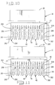
- Connector 20 including a solder tail spacer plate 22 having channels 42 with tapered sidewalls and solder tails 40 with sections tapered to conform thereto in accordance with the present invention is shown in Figure 1.
- Connector 20 includes a dielectric housing 24 molded of an appropriate plastic having mating face 26, opposed rear housing face 28 and mounting face 30 at a right angle to mating face 26.
- a plurality of contact receiving passages 32 extend from mating face 26 toward and opening onto rear housing face 28 with contacts 34 secured therein.
- Contacts 34 have a mating portion 36 extending into contact receiving passages 32 from rear housing face 28 that may be either pins or sockets and mounting portions 38, typically solder tails 40, that extend rearward from rear housing face 28 then are formed downward at a right angle to extend into and through a channel 42 in spacer plate 22.
- spacer plate 22 is molded to be integral with housing 24, although the invention is not limited thereto.
- a shielded version of connector 20 would include an electrically conductive member surrounding at least a portion of housing 24, such as die cast member 44 and drawn shell 46 as shown in Figure 3.
- spacer plate 22 is substantially parallel to contact receiving passages 32, is located below the lower row of passages 56 and extends rearwardly from rear housing face 28 of housing 24.
- Electrically conductive shell 46 has a similar outer profile to the formed raised portion 48 of housing 24.
- Shroud 50 extends forward from the die cast member 44 and conforms to and encloses the forward raised portion 48 of housing 24.
- Shroud 50 may have a trapezoidal or subminiature D shape to provide a polarization feature.
- Contacts 34 are formed on a strip on the desired centerline spacing.
- the contacts are received in two rows of contact receiving passages 54 and 56 and have mounting portions 38 formed to define four rows 58,60,62 and 64 of staggered solder tails 40.
- contacts 34 having formed mounting portions 38 are inserted into contact receiving passages 32 from rear housing face 28 substantially as disclosed in U.S. Patent 4,789,346, the disclosure of which is hereby incorporated by reference.
- the solder tail is passed into a respective channel 42 from rear face 52 of spacer plate 22.
- Mating portion 36 is secured in passage 32 by barbs 66 engaging sidewalls 68 in an interference fit.
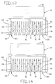
- FIG. 2 shows a top view of connector 20 without contacts 34 so that spacer plate 22 is more readily visible.
- Each channel 42 in the preferred embodiment has a pair of spaced detents 70, a forward detent 72 and a rearward detent 74, although the invention is not limited thereto.
- Each detent 70 in a channel 42 receives a respective solder tail from contacts 34 mounted one each in the contact receiving passages in rows 54 and 56 laterally aligned with channel 42.
- the staggering of solder tails 40 is achieved by positioning spaced detents 70 closer to rear housing face 28 in alternating channels 42, defining channels 42a than in the alternate channels 42 defining channels 42b.
- the detents form four rows of detents. All detents in each row of detents are spaced equidistant from rear housing face 28, and since rear face 52 is parallel to rear housing face 28, all detents in each row of detents are spaced equidistant from rear face 52.
- Contacts 34 designated contacts 34a when their solder tails are destined to be received in row 58, are pressed into alternate contact receiving passages 32 in the lower row 56 of passages; simultaneously the solder tails 40 of contacts 34a are pressed into respective channels 42a aligned with passages 32 and secured in the forward most detent 72.
- the solder tails of contacts 34a form row 58.
- contacts designated contacts 34b
- contacts 34b are pressed into the remaining alternate contact receiving passages 32 in the lower row 56 of passages; simultaneously, the solder tails 40 of contacts 34b are passed into respective channels 42b aligned with passages 32 and received in the forward most detent 72.
- the solder tails of contacts 34b form row 60.
- contacts designated contacts 34c are pressed into alternate contact receiving passages 32 in the upper row 54 of passages while simultaneously the solder tails 40 of contacts 34c are passed into respective channels 42a aligned with passages 32 and received in the rearward detent 74.
- the solder tails of contacts 34c form row 62.
- contacts designated contacts 34d are pressed into the remaining alternate contact receiving passages 32 in upper row 54 of passages; simultaneously, the solder tails 40 of contacts 34d are passed into respective channels 42b aligned with passages 32 and received in the rearward detent 74. The solder tails of contacts 34d form row 64.
- Each channel 42 has an opening onto rear face 52 that widens to facilitate insertion of solder tails 40 thereinto.
- the spacer plate is formed into beams integral with the spacer plate at forward end 78 thereof and extending to a free distal end proximate rear face 52.
- Channels 42a widen over a greater length of channel 42 than do channels 42b due to the rearward detent 74 being recessed farther into channels 42a than channels 42b.
- Figure 4 shows a typical mid-channel detent 70 in either of channels 42a or 42b in spacer plate 22.
- Figure 5 shows a typical forward most detent 72 in channel 42a.
- Figure 6 shows the cross section of a solder tail at the plane of the upper surface 76 of spacer plate 22.
- the leading surface 80 has beveled corners 82,84 to engage sidewalls of the channels during insertion of solder tails and to facilitate the beams adjacent to the channels to bias or deflect the beams to thereby permit passage of solder tail 40 therebetween.
- the trailing corners 86,88 are sharp.
- Each solder tail 40 may be secured in a detent 70 by a slight compression fit. A small lateral force may be maintained on each solder tail in a detent to assure that the solder tail is retained therein.
- Detent 70 is shaped substantially as the cross section of a solder tail 40, as best seen by comparing Figures 4 and 5 to Figure 6.
- Figures 7 and 8 show a solder tail 40 received in detents 70 of Figures 4 and 5 respectively.
- the beveled corners 82,84 are tapered to engage surfaces 96,98 of the channel sidewalls as a solder tail is pressed forward through the channel to pass through a detent.
- Sides 90 and 92 of solder tail 40 substantially engage sidewalls 100 and 102 of detent 70.
- Trailing corners 86,88 engage rear corners 104 and 106, which are slightly rounded due to the manufacturing process, in an interference fit. Trailing edge 94 of solder tail 40 is substantially against rearwalls 108,110.
- the spacer plate 22 between adjacent channels 42a and 42b form beams that bias or deflect laterally with an effective beam length when a solder tail 40 is passed into a channel 42 to be secured in a detent 70.
- Each beam extends from a distal end at rear face 52 forward to the depth of the channels adjacent to the beam where each beam is integral with spacer plate 22 at forward end 78.
- Contacts 34a are the first to be inserted into housing 24. With reference to Figures 2, 9 and 10, as contacts 34a are being inserted into a channel 42a, beam 122 is on the left and beam 120 is on the right. As solder tails 40 are passed between tapered lead-in surfaces 124, beam 122 is resiliently deflected laterally to the left and beam 120 is resiliently deflected laterally to the right with an effective beam length for both beams of length 126. Solder tails 40 then enter a first region 128 of channel 42a having substantially parallel walls. Solder tail 40 next enters rearward detent 74 whereupon beams 120 and 122 resile, returning toward their unbiased or undeflected position.
- Solder tail 40 enters and passes through a second region 130 of channel 42a having substantially parallel walls.
- Solder tail 40 then passes through a first transition region 132 in channel 42a that widens in the direction of insertion of solder tail 40, which again allows beams 120 and 122 to resile toward their unbiased position. Solder tail 40 then passes into and through a third region 134 of channel 42a having substantially parallel walls. As solder tail 40 passes through the third region, beams 120 and 122 remain in their substantially unbiased position.
- Solder tails 40 then pass through a second transition region 136 in channel 42a that narrows in the direction of insertion of solder tails 40.
- the reaction between the beveled corners 82,84 and the sidewalls of the transition region 136 cause beam 120 to again resiliently deflect or bias to the left and beam 122 to again resiliently deflect or bias to the right, both with an effective beam length of length 126.
- Solder tails 40 then move into and through a fourth region 138 of channel 42a having substantially parallel walls. Solder tails 40 of contacts 34a then enter forward detent 72 of channel 42a whereupon beams 120 and 122 resile, returning toward their unbiased or undeflected position to secure solder tail 40 in forward detent 72.
- contacts 34b which are inserted into channel 42b.
- beam 120 is on the left and beam 122 is on the right.
- solder tails of contacts 34a are secured in detent 72 of channels 42a.
- solder tails 40 are pressed between tapered lead-in surfaces 144, beam 120 is resiliently deflected laterally to the left and beam 122 is resiliently deflected laterally to the right with an effective beam length of length 146 since the solder tails 40 of contacts 34a are in forward detents 72 of the adjacent channels 42a. Solder tails 40 then enter and pass through a first region 148 of channels 42b having substantially parallel walls. Solder tails 40 next enter rearward detent 74 whereupon beams 122 and 120 resile, returning toward their unbiased or undeflected position.
- Solder tail 40 then enters and passes through a second region 150 of channel 42b having substantially parallel walls. Solder tail 40 then passes through a first transition region 152 in channel 42b that widens in the direction of insertion of solder tail 40, which again allows beams 122 and 120 to resile toward their unbiased position. Solder tails 40 then pass into and through a third region 154 of channel 42b having substantially parallel walls.
- Solder tails 40 then pass through a second transition region 156 in channel 42b that narrows in the direction of insertion solder posts 40.
- the reaction between beveled corners 82,84 and the sidewalls of transition region 156 cause beam 120 to again resiliently deflect or bias to the left and beam 122 to again resiliently deflect or bias to the right, both with an effective beam length of length 146.
- Solder tails 40 then move into and through a fourth region 158 of channel 42b having substantially parallel walls. Solder tails 40 of contact 34b then enter forward detent 72 of channel 42b whereupon beams 122 and 120 resile, returning toward their unbiased or undeflected position to secure solder tail 40 and forward detent 72.
- contacts 32c which are inserted into channels 42a.
- beam 122 is on the left and beam 120 is on the right.
- solder tails 40 are passed between tapered lead-in surfaces 144, beam 122 is resiliently deflected laterally to the left and beam 120 is resiliently deflected laterally to the right with an effective beam length of length 166 since there is a solder tail 40 of contact 34b in forward detents 72 of channels 42b adjacent to each channel 42a.
- Solder tails 40 enter first region 128 of channels 42a then pass into rearward detent 74 whereupon beams 120 and 122 resile, returning toward their unbiased or undeflected position to secure solder tails 40 of contacts 34c in rearward detents 74 of channels 42a.
- contacts 34d which are inserted into channels 42b.
- beam 120 is on the left and beam 122 is on the right.
- solder tails 40 are passed between tapered lead-in surfaces 144, beam 120 is resiliently deflected laterally to the left and beam 122 is resiliently deflected laterally to the right with an effective beam length of length 176.
- Solder tails 40 pass through first region 148 of channel 42b and enter rearward detent 74 whereupon beams 120 and 122 resile returning toward their unbiased or undeflected position to secure solder tails 40 of contacts 34d in rearward detents 74 of channels 42b.
- forward detents 72 in channels 42a are laterally aligned and form row 58.
- the forward detents 72 in channels 42b are laterally aligned and form row 60.
- the rearward detent 74 in channels 42a are laterally aligned and form row 62.
- the rearward detent 74 in channels 42b are laterally aligned and form row 64. In this manner, the two rows 54 and 56 of mating portions of contacts 34 have staggered solder tails forming four rows.
- spacer plate 22 has a slot 200 between the final lateral slot 42 and substantially rigid flange 202.
- Endwall 198 integral with and extending perpendicular to flange 202 enhances the rigidity of flange 202.
- Slot 200 defines a beam 204 which may be considered a beam 120 or a beam 122 as described above depending upon whether the channel adjacent to slot 200 is a channel 42a or a channel 42b. As shown in Figure 2, channel 42b is adjacent slot 200 defining beam 204 therebetween.
- Beam 204 has the characteristics of a beam 122. Absent slot 200, beam 204 would be a portion of flange 202 and would be, like flange 202, substantially rigid.
- Beam 204 is bridged to flange 202 at bridging member 206 interrupting slot 200 into forward slot 208 and rear slot 210 and dividing beam 204 into forward beam 212 and rear beam 214.
- Bridging member 206 is positioned along slot 200 forward of the rearward detent 74, that is spaced away from rear face 52 toward mating face 26, in the adjacent channel 42, laterally aligned with the rearward detent 74 in the channel 42 adjacent to the channel 42 that is adjacent to slot 200.
- the channel 42 adjacent to slot 200 will be referred to as channel 242 and the channel 42 adjacent to channel 242 will be referred to as channel 244.
- bridging member 206 is positioned along slot 200 forward of the rearward detent 74 in channel 242 and laterally aligned with rearward detent 74 in channel 244.
- bridging member 206 spans a distance along slot 200 that is substantially the thickness of a solder tail to be received in a detent in one of the channels.
- slot 200 extends into spacer plate 22 from rear face 52, substantially parallel to and substantially the same distance as slots 42.
- Beam 204 has the same mass as beam 122 and in this manner, beam 204 will exhibit the same characteristics as a beam 122 during insertion of solder tails 40 of contacts 34c and 34d of spacer plate 22.
- beam 120 functions as described above. While solder tail 40 is passing between tapered lead-in surfaces 124 and first region 128, beam 204 and more specifically rear beam 214 is resiliently deflected to the left with an effective beam length of length 166 due to beam 204 being bridged to flange 202 by bridging member 206. As solder tail 40 is received in rearward detent 74, rear beam 214 resiles, returning toward its unbiased or undeflected position.
- rear beam 214 is again resiliently deflected to the left with an effective beam length of length 166 then resiles to an unbiased position. Note also that forward beam 212 may flex toward channel 242 since there is no contact in forward detent 70 of channel 242.
- solder tail 40 passes freely through third region 134.
- forward beam 212 resiliently bows into forward slot 208.
- forward beam 212 resiles toward its unbiased position to secure solder tail 40 in detent 72.
- a small lateral force may be maintained on solder tail 40 of contact 34a to assure that the solder tail is retained in detent 72.
- beam 120 on one side of channel 242 functions as described above and beam 204 on the other side of channel 242 functions like a beam 122 as described above due to solder tail 40 of contacts 34b present in forward detent 72 of channel 244, the design of beam 204 to have the same spring characteristics of beam 122, such as by having the same mass or shape, and the presence and location of bridging member 206 in slot 200.
- beam 120 is resiliently deflected to the right with an effective beam length of length 166.
- beam 204 is resiliently deflected to the left also with an effective beam length of length 166; forward beam 212 is effectively prevented from bowing due to the presence of solder tail 40 of contact 34a and forward detent 72 of channel 242.
- beam 204 on one side of channel 242 deflects with the same beam length as beam 120 on the other side of channel 242, with the effective beam length of beam 204 determined by the presence and location of bridging member 206.
- solder tail 40 of contact 34c is received in detent 74 of channel 242, beams 120 and 204 resile toward their unbiased or undeflected position to secure solder tail 40 of contact 34c in rear detent 74 of channel 242.
- a small lateral force may be maintained on solder tail 40 of contact 34c to assure that the solder tail is maintained in detent 74. Since the effective length of beam 204 that secures solder tail 40 of contact 34c in position is the same as the effective length of any beam 120 or 122 securing any of the solder tails of other contacts 34c in rearward detents 74 of channels 42a, the normal force applied by each beam holding each of the solder tails in a detent 74 in row 62 is substantially equal.
- bridge member 206 in slot 200 emulates the presence of a solder tail with respect to a rear solder tail in an adjacent channel being inserted and with respect to securing a solder tail in a rearward detent rearward of the bridge member 206 in an adjacent channel 242 in spacer plate 22 wherein the adjacent channel is adjacent to slot 200. Furthermore, the presence of bridging member 206 assures equal lateral normal force on each of the solder tails in a row of solder tails as retained in spacer plate 22.
- beam 204 has been described in the preferred embodiment as being bridged to flange 202 thereby interrupting slot 200, a protrusion extending from flange 202 toward beam 204 or a protrusion extending from beam 204 toward flange 202 or some combination thereof could provide the same function of emulating the presence of a contact to prevent substantial lateral movement of the beam due to the presence of the protrusion between beam 204 and flange 202.
- spacer plate 22 has a slot 300 between the final lateral slot 42 and substantially rigid flange 302.
- Slot 300 defines a beam 304 which may be either a beam 120 or a beam 122 as described above depending upon whether the channel adjacent to slot 300 is a channel 42a or a channel 42b.
- channel 42a is adjacent to slot 300 thereby defining beam 304 having the characteristics of a beam 120. Absent slot 300, beam 304 would be a portion of flange 302 and would be, like flange 302, substantially rigid.
- Beam 304 is bridged to flange 302 by bridging member 306 interrupting slot 300 into forward slot 308 and rear slot 310 as well as dividing beam 304 into forward beam 312 and rear beam 314.
- Bridging member 306 is positioned along slot 300 forward of rearward detent 74, that is spaced away from rear face 52 toward mating face 26, in the adjacent channel 42, laterally aligned with the rearward detent 74 in the channel 42 adjacent to the channel 42 adjacent to slot 300.
- the channel 42 adjacent to slot 300 will be referred to as channel 342 and the channel 42 adjacent to channel 342 will be referred to as channel 344.
- Channel 342 is similar to a channel 42b and channel 344 is similar to a channel 42a.
- bridging member 306 is positioned along slot 300 forward of the rearward detent 74 in channel 342 and laterally aligned with rearward detent 74 in channel 344.
- bridging member 306 spans a distance along slot 300 that is substantially the thickness of a solder tail to be received in a detent in one of the channels.
- slot 300 extends into spacer plate 22 from rear face 52 substantially parallel to and substantially the same distance as slots 42.
- Beam 304 has the same mass as a beam 120 and in this manner will exhibit the same spring characteristics as beam 120 during insertion of solder tails 40 of contacts 34c and 34d into slot 342 and during retention of solder tails 40 of contacts 34c and 34d in detents 70 of slot 342.
- beam 120 functions as described above. While solder tail 40 is passing between tapered lead-in surfaces 144 and first region 148, beam 304, and more specifically rear beam 314, is resiliently deflected to the right with an effective beam length of length 176 due to beam 304 being bridged to flange 302 by bridging member 306. As solder tail 40 is received in rearward detent 74, rear beam 314 resiles returning toward its unbiased or undeflected position.
- rear beam 314 is again resiliently deflected to the right with an effective beam length of length 176 then resiles to its unbiased position. Note also that forward beam 312 may flex toward channel 342 as tail 40 is moved through second region 150 and first transition 152 since there is no solder tail in forward detent 72 of channel 342.
- solder tail 40 passes freely through third region 154.
- forward beam 312 resiliently bows into forward slot 308.
- forward beam 312 Upon solder tail 40 of contact 34b moving into forward detent 72 in channel 342, forward beam 312 resiles toward its unbiased position to secure solder tail 40 in detent 72.
- a small lateral force may be maintained on solder tail 40 of contact 34b to assure that the solder tail is maintained in detent 70.
- beam 120 on one side of channel 342 functions as described above and beam 304 on the other side of channel 342 functions like a beam 122 as described above due to solder tail 40 of contact 34c being present in rear detent 74 of channel 344, the design of beam 304 to have the same mass and spring characteristics of a beam 122 and the presence of and location of bridging member 306 in slot 300.
- beam 120 is resiliently deflected to the left with an effective beam length of length 176.
- beam 304 is resiliently deflected to the right also with an effective beam length of length 176; forward beam 312 is effectively prevented from bowing due to the presence of solder tail 40 of contact 34b in forward detent 72 of channel 342.
- beam 304 on one side of channel 342 deflects with the same effective beam length as beam 122 on the other side of channel 342, with the effective length of beam 304 determined by the presence and location of bridging member 306.
- solder tail 40 of contact 34d is received in rearward detents 74 of channel 342, beams 120 and 304 resile toward their unbiased or undeflected position to secure solder tail 40 of contact 34d in rear detent 74 of channel 342.
- a small lateral force may be maintained on solder tail 40 of contact 34d to assure the solder tail is maintained in detent 74. Since the effective length of beam 304 that secures solder tail 40 of contact 34d in detent 74 is the same as the effective length of any beam 120 or 122 securing any of the other solder tails of contacts 34d in a rearward detent of a channel 42b, the normal force applied by each beam holding each of the solder tails in a rearward detent is substantially equal.
- bridge member 306 in slot 300 emulates the presence of a solder tail with respect to securing a solder tail in a rearward detent, rearwardly of bridging member 306, in a channel of spacer plate 22 adjacent to slot 300. Furthermore, the presence of bridging member 306 assures equal lateral normal force on each of the solder tails in a row of solder tails as retained in spacer plate 22.
- beam 304 has been described in the preferred embodiment as being bridged to flange 302 thereby interrupting slot 300, a protrusion extending from flange 302 toward beam 304 or a protrusion extending from beam 304 toward flange 302 or some combination thereof could provide the same function of emulating the presence of a contact to prevent substantial lateral movement of the beam due to the presence of the protrusion between beam 304 and flange 302.
- Beams 204 and 304 have been described as having the same mass as a beam 120 or 122 which they represent in the spacer plate. While beams 204 and 304 in the preferred embodiment do not have the profile of beams 120 or 122 on the side thereof that forms slot 200 or 300, they could have such a profile and thereby be assured to have the same mass and spring characteristics as beams 120 or 122. To obtain the same mass, the sidewall of the slot forming the beam 204 or 304 is shifted until the mass of the respective beam 204 or 304 equals the mass of a beam 120 or 122 which they represent.
- Figure 14 shows a top view of a connector having all of the contact solder tails (shown in cross section) received in spacer plate 22.
- Figure 15 shows a partial sectional view of a channel 42, taken from a detent 70 and looking rearward in a channel, taken along the lines 15-15 in Figure 2. From this view it can be seen that the sidewalls 400,402 of channels 42 are tapered through the thickness of spacer plate 22 from top surface 76 to lower surface 404. Angle 406 between either sidewall 400 or 402 and the vertical in Figure 15 forms an angle of five (5) degrees.
- the sidewalls 100,102 of a detent 70 may or may not be angled at the same angle as sidewalls 400,402. As shown in Figure 15, sidewalls 100,102 through the region of a detent form an angle 410 with respect to the vertical of two and one half (2.5) degrees.
- Figure 16 shows a typical contact 34a or 34b, with a middle section removed, before the solder tail is formed proximate line 412 to be substantially perpendicular to mating portion 36.
- Formed contacts 34a and 34b are shown in Figure 1 and are formed by bending solder tail 40 as shown in Figure 16 out of the paper toward the reader.
- Contacts 34a and 34b have stop protrusions 414 and 416 spaced from distal end 418. Stop protrusions 414,416 extend laterally respectively from sides 90,92 to a tip-to-tip width that exceeds the spacing of the channel defining sidewalls, sidewalls 400,402 in the absence of detents or sidewalls 100,102 when detents are present, where the solder tail is positioned in the assembled connector. In this manner, each protrusion extends beyond a respective sidewall 100,102 in the detent, as best seen in Figure 17.
- solder tail 40 is tapered through region 420 that is received in a channel of a spacer plate.
- region 420 is above stop protrusions 414 and 416 which are positioned below lower surface 404 upon contact 34a or 34b being inserted into the housing.
- the taper of sides 90 and 92 of solder tail 40 through region 420 conforms to the taper of sidewalls 100,102 of the detent in which the solder tail is received.
- any upward displacement of the solder tail of a contact 34a or 34b would wedge solder tail 40 in the detent.
- sides 90 and 92 would engage sidewalls 100,102 with increasing normal force, thereby increasingly resisting any further upward displacement of the solder tail.
- stop protrusions 416 and 418 prevent any substantial upward movement in accordance with U.S. Patent 4,842,528, the disclosure of which is hereby incorporated by reference.
- Figure 18 shows a typical contact 34c or 34d, with a middle section removed, before the solder tail is formed proximate line 436 to be substantially perpendicular to mating portion 36.
- Formed contacts 34c and 34d are shown in Figure 1 and are formed by bending solder tail 40 as shown in Figure 18 out of the taper toward the reader.
- Contacts 34c and 34d have lower stop protrusions 438 and 440 spaced from distal end 442.
- the lower stop protrusions extend laterally respectively from sides 90,92 of a solder tail of a contact 34c or 34d substantially like stop protrusions 414 and 416, to perform the same functions for contacts 34c or 34d that stop protrusions 414 and 416 perform with respect to contacts 34a or 34b.
- Solder tails 34c and 34d have upper stop protrusions 444 and 446 spaced upwardly along solder tail 40 from the lower stop protrusions at least the thickness of spacer plate 22.
- Upper stop protrusions 444 and 446 extend laterally respectively from sides 90,92 to a tip-to-tip width that exceeds the spacing of channel defining sidewalls where the solder tail is positioned in the assembled connector.
- Upper stop protrusions 444 and 446 substantially prevent solder tail 40 from moving downwardly into spacer plate 22.
- Contacts 34c and 34d are more susceptible to downward movements in spacer plate 22 than are contacts 34a and 34b as contacts 34c and 34d are exposed behind rear housing face 28.
- lower stop protrusions 438 and 440 are positioned below lower surface 404 of the spacer plate and upper stop protrusions 444 and 446 are positioned above upper surface 76 of the spacer plate when contact 34c or 34d is being inserted into or is secured in the connector.
- lower stop protrusions 438 and 440 provide a back-up stop that prevents any large movement of solder tail 40 upward through spacer plate 22.
- Upper stop protrusions 444 and 446 substantially prevent downward movement of solder tail 40 through spacer plate 22 in accordance with the teaching of U.S. Patent 4,842,528.
Landscapes
- Coupling Device And Connection With Printed Circuit (AREA)
- Multi-Conductor Connections (AREA)
- Casings For Electric Apparatus (AREA)
Applications Claiming Priority (2)
| Application Number | Priority Date | Filing Date | Title |
|---|---|---|---|
| US620605 | 1984-06-14 | ||
| US07/620,605 US5071372A (en) | 1990-11-30 | 1990-11-30 | Connector with contact spacer plate having tapered channels |
Publications (3)
| Publication Number | Publication Date |
|---|---|
| EP0488349A2 true EP0488349A2 (de) | 1992-06-03 |
| EP0488349A3 EP0488349A3 (en) | 1992-07-01 |
| EP0488349B1 EP0488349B1 (de) | 1996-04-17 |
Family
ID=24486592
Family Applications (1)
| Application Number | Title | Priority Date | Filing Date |
|---|---|---|---|
| EP91120487A Expired - Lifetime EP0488349B1 (de) | 1990-11-30 | 1991-11-29 | Verbinder mit Kontaktabstandsplatte mit keilförmigen Kanälen |
Country Status (4)
| Country | Link |
|---|---|
| US (1) | US5071372A (de) |
| EP (1) | EP0488349B1 (de) |
| DE (1) | DE69118828T2 (de) |
| ES (1) | ES2085946T3 (de) |
Families Citing this family (13)
| Publication number | Priority date | Publication date | Assignee | Title |
|---|---|---|---|---|
| JPH0583900A (ja) * | 1991-07-25 | 1993-04-02 | Mabuchi Motor Co Ltd | 小型モータおよびその製造方法 |
| US5358413A (en) * | 1992-12-08 | 1994-10-25 | The Whitaker Corporation | Right-angle board-mountable electrical connector with precision terminal positioning |
| US5458510A (en) * | 1993-12-03 | 1995-10-17 | High Voltage Engineering Corporation | Printed circuit board connector contact |
| JPH08124638A (ja) * | 1994-10-20 | 1996-05-17 | Amp Japan Ltd | 表面実装型コネクタ及びその電気コンタクト |
| US5725386A (en) * | 1996-05-24 | 1998-03-10 | The Whitaker Corporation | Board-mountable electrical connector |
| US5779489A (en) * | 1996-05-24 | 1998-07-14 | The Whitaker Corporation | Board mountable electrical connector |
| JPH1021984A (ja) * | 1996-06-28 | 1998-01-23 | Yazaki Corp | コネクタ端子の圧入構造 |
| JP3681044B2 (ja) | 1999-06-02 | 2005-08-10 | 矢崎総業株式会社 | 基板用コネクタ |
| JP4425730B2 (ja) * | 2003-07-09 | 2010-03-03 | 株式会社オートネットワーク技術研究所 | コネクタ端子の製造方法 |
| US7604518B2 (en) * | 2007-11-26 | 2009-10-20 | Tyco Electronics Corporation | Electrical contact with retention latch |
| CN106363312B (zh) * | 2016-11-23 | 2019-03-08 | 京信通信技术(广州)有限公司 | 焊接基体 |
| EP3618194B1 (de) * | 2018-08-27 | 2024-10-02 | Aptiv Technologies AG | Elektrischer stecker |
| JP7428972B2 (ja) * | 2020-08-25 | 2024-02-07 | 住友電装株式会社 | コネクタ |
Citations (3)
| Publication number | Priority date | Publication date | Assignee | Title |
|---|---|---|---|---|
| GB2176950A (en) * | 1985-06-21 | 1987-01-07 | Harwin Engineers S A | Socket assembly for mounting in P.C.B. hole |
| US4842528A (en) * | 1987-03-27 | 1989-06-27 | Amp Incorporated | Solder post retention means |
| DE9002176U1 (de) * | 1990-02-23 | 1990-04-26 | Siemens AG, 1000 Berlin und 8000 München | Einpreßkontaktelement |
Family Cites Families (12)
| Publication number | Priority date | Publication date | Assignee | Title |
|---|---|---|---|---|
| NL302726A (de) * | 1963-02-18 | |||
| US3493916A (en) * | 1967-07-24 | 1970-02-03 | Molex Products Co | Printed circuit board terminal and connector |
| US3551877A (en) * | 1968-11-20 | 1970-12-29 | Hugh H Eby Co | Electrical connector |
| US4080041A (en) * | 1977-03-14 | 1978-03-21 | International Telephone And Telegraph Corporation | Electrical connector |
| US4225209A (en) * | 1979-05-18 | 1980-09-30 | Amp Incorporated | Electrical connector receptacle |
| JPS58175926A (ja) * | 1982-04-05 | 1983-10-15 | 日本電気ホームエレクトロニクス株式会社 | 出力回路の保護方法 |
| US4491376A (en) * | 1982-09-20 | 1985-01-01 | General Motors Corporation | Electrical header assembly |
| DE3318135A1 (de) * | 1983-05-18 | 1984-11-22 | Erni Elektroapparate Gmbh, 7321 Adelberg | Loetfreie elektrische verbindung |
| US4660911A (en) * | 1985-12-06 | 1987-04-28 | Amp Incorporated | Surface mount connector |
| US4697864A (en) * | 1986-06-19 | 1987-10-06 | Amp Incorporated | Printed circuit board receptacle for sealed connector |
| US4789346A (en) * | 1987-03-27 | 1988-12-06 | Amp Incorporated | Solder post alignment and retention system |
| US4842554A (en) * | 1988-06-03 | 1989-06-27 | Amp Incorporated | One-piece shield for a circular din |
-
1990
- 1990-11-30 US US07/620,605 patent/US5071372A/en not_active Expired - Lifetime
-
1991
- 1991-11-29 EP EP91120487A patent/EP0488349B1/de not_active Expired - Lifetime
- 1991-11-29 DE DE69118828T patent/DE69118828T2/de not_active Expired - Fee Related
- 1991-11-29 ES ES91120487T patent/ES2085946T3/es not_active Expired - Lifetime
Patent Citations (3)
| Publication number | Priority date | Publication date | Assignee | Title |
|---|---|---|---|---|
| GB2176950A (en) * | 1985-06-21 | 1987-01-07 | Harwin Engineers S A | Socket assembly for mounting in P.C.B. hole |
| US4842528A (en) * | 1987-03-27 | 1989-06-27 | Amp Incorporated | Solder post retention means |
| DE9002176U1 (de) * | 1990-02-23 | 1990-04-26 | Siemens AG, 1000 Berlin und 8000 München | Einpreßkontaktelement |
Also Published As
| Publication number | Publication date |
|---|---|
| DE69118828D1 (de) | 1996-05-23 |
| EP0488349B1 (de) | 1996-04-17 |
| US5071372A (en) | 1991-12-10 |
| DE69118828T2 (de) | 1996-09-05 |
| EP0488349A3 (en) | 1992-07-01 |
| ES2085946T3 (es) | 1996-06-16 |
Similar Documents
| Publication | Publication Date | Title |
|---|---|---|
| US5080596A (en) | Connector with contact spacer plate providing greater lateral force on rear contacts | |
| EP0488298B1 (de) | Verbinder mit Kontaktdistanzierplatte mit gleichförmiger seitlicher Kraft | |
| EP0306523B1 (de) | System zur ausrichtung und arretierung von lötstiften | |
| US4842528A (en) | Solder post retention means | |
| EP0555963B1 (de) | Stecker mit einteiligem Massestreifen | |
| EP0436943B1 (de) | Verbesserter Leiterplattenrandverbinder | |
| US5810623A (en) | Edge connector for a printed circuit board | |
| US5848920A (en) | Fabrication of electrical terminals for edge card connectors | |
| US6244910B1 (en) | Electrical box contact with stress limitation | |
| EP0488349B1 (de) | Verbinder mit Kontaktabstandsplatte mit keilförmigen Kanälen | |
| US5586915A (en) | Electrical connector with contacts at different insertion depths | |
| US5542851A (en) | Electrical connector with improved grounding | |
| AU591635B2 (en) | Electrical connector | |
| EP0487866B1 (de) | Elektrische Verbinderanordung zum Montieren auf gedruckter Leiterplatte | |
| EP0657959B1 (de) | Elektrische Verbinderanordnung zum Montieren auf gedruckte Leiterplatten | |
| US5785556A (en) | Edge connector for a printed circuit board | |
| US4752246A (en) | Preloaded spring contact electrical terminal | |
| US5800213A (en) | Edge connector for a printed circuit board | |
| EP0806813B1 (de) | Elektrischer Steckverbinder mit verbesserten Kontaktstückhaltemitteln | |
| US5190483A (en) | Contact retention | |
| EP0374307B1 (de) | Verbinderanordnung für gedruckte Leiterplatte | |
| JP2816435B2 (ja) | コンタクトスペーサ付き電気コネクタ | |
| US5800203A (en) | Terminal retention for an electrical connector |
Legal Events
| Date | Code | Title | Description |
|---|---|---|---|
| PUAI | Public reference made under article 153(3) epc to a published international application that has entered the european phase |
Free format text: ORIGINAL CODE: 0009012 |
|
| PUAL | Search report despatched |
Free format text: ORIGINAL CODE: 0009013 |
|
| AK | Designated contracting states |
Kind code of ref document: A2 Designated state(s): DE ES FR GB IT NL |
|
| AK | Designated contracting states |
Kind code of ref document: A3 Designated state(s): DE ES FR GB IT NL |
|
| RAP1 | Party data changed (applicant data changed or rights of an application transferred) |
Owner name: THE WHITAKER CORPORATION |
|
| 17P | Request for examination filed |
Effective date: 19921230 |
|
| 17Q | First examination report despatched |
Effective date: 19940816 |
|
| GRAH | Despatch of communication of intention to grant a patent |
Free format text: ORIGINAL CODE: EPIDOS IGRA |
|
| GRAA | (expected) grant |
Free format text: ORIGINAL CODE: 0009210 |
|
| AK | Designated contracting states |
Kind code of ref document: B1 Designated state(s): DE ES FR GB IT NL |
|
| ITF | It: translation for a ep patent filed | ||
| REF | Corresponds to: |
Ref document number: 69118828 Country of ref document: DE Date of ref document: 19960523 |
|
| REG | Reference to a national code |
Ref country code: ES Ref legal event code: FG2A Ref document number: 2085946 Country of ref document: ES Kind code of ref document: T3 |
|
| ET | Fr: translation filed | ||
| PLBE | No opposition filed within time limit |
Free format text: ORIGINAL CODE: 0009261 |
|
| STAA | Information on the status of an ep patent application or granted ep patent |
Free format text: STATUS: NO OPPOSITION FILED WITHIN TIME LIMIT |
|
| 26N | No opposition filed | ||
| PGFP | Annual fee paid to national office [announced via postgrant information from national office to epo] |
Ref country code: NL Payment date: 19980914 Year of fee payment: 8 |
|
| PGFP | Annual fee paid to national office [announced via postgrant information from national office to epo] |
Ref country code: ES Payment date: 19981119 Year of fee payment: 8 |
|
| PG25 | Lapsed in a contracting state [announced via postgrant information from national office to epo] |
Ref country code: ES Free format text: LAPSE BECAUSE OF NON-PAYMENT OF DUE FEES Effective date: 19991130 |
|
| PG25 | Lapsed in a contracting state [announced via postgrant information from national office to epo] |
Ref country code: NL Free format text: LAPSE BECAUSE OF NON-PAYMENT OF DUE FEES Effective date: 20000601 |
|
| NLV4 | Nl: lapsed or anulled due to non-payment of the annual fee |
Effective date: 20000601 |
|
| REG | Reference to a national code |
Ref country code: GB Ref legal event code: IF02 |
|
| PGFP | Annual fee paid to national office [announced via postgrant information from national office to epo] |
Ref country code: GB Payment date: 20031002 Year of fee payment: 13 |
|
| PGFP | Annual fee paid to national office [announced via postgrant information from national office to epo] |
Ref country code: FR Payment date: 20031105 Year of fee payment: 13 |
|
| PGFP | Annual fee paid to national office [announced via postgrant information from national office to epo] |
Ref country code: DE Payment date: 20031128 Year of fee payment: 13 |
|
| REG | Reference to a national code |
Ref country code: ES Ref legal event code: FD2A Effective date: 20001214 |
|
| PG25 | Lapsed in a contracting state [announced via postgrant information from national office to epo] |
Ref country code: GB Free format text: LAPSE BECAUSE OF NON-PAYMENT OF DUE FEES Effective date: 20041129 |
|
| PG25 | Lapsed in a contracting state [announced via postgrant information from national office to epo] |
Ref country code: DE Free format text: LAPSE BECAUSE OF NON-PAYMENT OF DUE FEES Effective date: 20050601 |
|
| GBPC | Gb: european patent ceased through non-payment of renewal fee |
Effective date: 20041129 |
|
| PG25 | Lapsed in a contracting state [announced via postgrant information from national office to epo] |
Ref country code: FR Free format text: LAPSE BECAUSE OF NON-PAYMENT OF DUE FEES Effective date: 20050729 |
|
| REG | Reference to a national code |
Ref country code: FR Ref legal event code: ST |
|
| PG25 | Lapsed in a contracting state [announced via postgrant information from national office to epo] |
Ref country code: IT Free format text: LAPSE BECAUSE OF NON-PAYMENT OF DUE FEES;WARNING: LAPSES OF ITALIAN PATENTS WITH EFFECTIVE DATE BEFORE 2007 MAY HAVE OCCURRED AT ANY TIME BEFORE 2007. THE CORRECT EFFECTIVE DATE MAY BE DIFFERENT FROM THE ONE RECORDED. Effective date: 20051129 |