EP0487184A2 - Circuit for recording and reproducing time base error corrector reference signal - Google Patents
Circuit for recording and reproducing time base error corrector reference signal Download PDFInfo
- Publication number
- EP0487184A2 EP0487184A2 EP91306616A EP91306616A EP0487184A2 EP 0487184 A2 EP0487184 A2 EP 0487184A2 EP 91306616 A EP91306616 A EP 91306616A EP 91306616 A EP91306616 A EP 91306616A EP 0487184 A2 EP0487184 A2 EP 0487184A2
- Authority
- EP
- European Patent Office
- Prior art keywords
- reference signal
- signal
- tbc
- video signal
- circuit
- Prior art date
- Legal status (The legal status is an assumption and is not a legal conclusion. Google has not performed a legal analysis and makes no representation as to the accuracy of the status listed.)
- Granted
Links
Images


Classifications
-
- G—PHYSICS
- G11—INFORMATION STORAGE
- G11B—INFORMATION STORAGE BASED ON RELATIVE MOVEMENT BETWEEN RECORD CARRIER AND TRANSDUCER
- G11B20/00—Signal processing not specific to the method of recording or reproducing; Circuits therefor
- G11B20/10—Digital recording or reproducing
- G11B20/18—Error detection or correction; Testing, e.g. of drop-outs
-
- H—ELECTRICITY
- H04—ELECTRIC COMMUNICATION TECHNIQUE
- H04N—PICTORIAL COMMUNICATION, e.g. TELEVISION
- H04N9/00—Details of colour television systems
- H04N9/79—Processing of colour television signals in connection with recording
- H04N9/87—Regeneration of colour television signals
- H04N9/89—Time-base error compensation
-
- H—ELECTRICITY
- H04—ELECTRIC COMMUNICATION TECHNIQUE
- H04N—PICTORIAL COMMUNICATION, e.g. TELEVISION
- H04N9/00—Details of colour television systems
- H04N9/79—Processing of colour television signals in connection with recording
- H04N9/80—Transformation of the television signal for recording, e.g. modulation, frequency changing; Inverse transformation for playback
- H04N9/82—Transformation of the television signal for recording, e.g. modulation, frequency changing; Inverse transformation for playback the individual colour picture signal components being recorded simultaneously only
- H04N9/8205—Transformation of the television signal for recording, e.g. modulation, frequency changing; Inverse transformation for playback the individual colour picture signal components being recorded simultaneously only involving the multiplexing of an additional signal and the colour video signal
- H04N9/8211—Transformation of the television signal for recording, e.g. modulation, frequency changing; Inverse transformation for playback the individual colour picture signal components being recorded simultaneously only involving the multiplexing of an additional signal and the colour video signal the additional signal being a sound signal
- H04N9/8222—Transformation of the television signal for recording, e.g. modulation, frequency changing; Inverse transformation for playback the individual colour picture signal components being recorded simultaneously only involving the multiplexing of an additional signal and the colour video signal the additional signal being a sound signal using frequency division multiplex
Definitions
- the present invention relates to a time base error corrector (TBC) for correcting timing discordance of video signals in video signal recording/reproducing systems, and more particularly to a circuit for recording and reproducing a reference signal used for correcting timing discordance of video signals.
- TBC time base error corrector
- a video signal includes video information arranged in accordance with a synchronizing signal so as to display accurate images on display devices, and is affected by noise during recording and reproducing through a recording medium as are any other information signals, thereby producing time base errors in the video information.
- Time base errors occur mainly due to mechanical elements included in the recording/reproducing apparatus, which can tire viewers due to trembling of an image caused by the temporal lengthening or shortening of the signal.
- an analogue video signal is converted to a digital video signal for digitally processing the analogue video signal
- a variation in the sampling number may occur due to the time base error, though the number of samples for each synchronization is required to be constant.
- video information designated for each pixel may move to the left or to the right by several pixels, so that the phase of the signal is not fixed and furthermore, signal processing between frames becomes impossible due to the changing pixel positions.
- a time base error corrector (hereinafter referred to as a TBC) is an apparatus that corrects the timing discordance of video information due to time base error of the video signal, and which is employed to remove the time base errors created during recording and reproducing and to resynchronize the signal more precisely in video recording and reproducing systems.
- analog to digital converter (A/D converter) 10 samples by a certain period and encodes a video signal entering through input line 5, thereby generating a digital video signal.
- Memory 20 temporarily stores the digital video signal converted in the A/D converter 10.
- Digital to analog converter (D/A converter) 30 converts the digital video signal read-out from the memory 20 to an analog video signal and outputs it through output line 15.
- storing clock generator 40 generates storing clocks having different periods according to the period variation of a horizontal synchronizing signal of a video signal supplied through input line 5 and supplies the storing clocks to A/D converter 10 and memory 20.
- Reading clock generator 50 generates a reading clock having a certain period and supplies the clock to memory 20 and D/A converter 30.
- synchronizing signal separator 41 separates a horizontal synchronizing signal from a video signal supplied through input line 5 and phase comparator 42 compares the phase of the frequency-divided storing clock applied from frequency divider 44 with that of the horizontal synchronizing signal supplied from the synchronizing signal separator 41 and generates a control voltage corresponding to the phase difference.
- Voltage controlled oscillator 43 (hereinafter referred to as VCO) generates storing clocks having different frequencies depending on the control voltages applied from the phase comparator 42 and supplies the clocks to A/D converter 10, memory 20 and frequency divider 44.
- the frequency divider 44 frequency-divides the storing clocks in order that the clocks have the same frequency as that of the horizontal synchronizing signal and supplies the clocks to phase comparator 42.
- the conventional TBC shown in Figure 1 samples a video signal by a certain number of samplings for each horizontal synchronizing period by regulating (adding/subtracting) the frequency of the storing clock according to the period variation of the horizontal synchronizing signal and stores the video signal into the memory. Then, such video data stored in the memory is read-out by the reading clock of a certain frequency and is converted to an analog video signal to correct the timing discordance of the video information of the video signals.
- a negative feedback circuit is provided between the phase comparator 42 and the VCO in order to regulate (add/subtract) the frequency of the storing clock for every horizontal synchronizing signal period.
- the time constant of the negative feedback circuit usually has a time period which is at least greater than the horizontal synchronizing signal period and usually of two or three times the horizontal synchronizing signal period.
- Preferred embodiments of the present invention aim to provide a circuit for recording and reproducing a TBC reference signal, in a video recording/reproducing system, which records a TBC reference signal with a video signal on a recording medium, and then corrects the time base errors of the video signal by the reproduced TBC reference signal so that precise time base error correction is attained.
- a circuit for recording/reproducing a TBC reference signal in video recording/reproducing systems including a recorder for recording a video signal on a recording medium and a reproducer for reproducing the video signal recorded on the recording medium and correcting the time base error, the circuit comprising: adding means included in said recorder and used for adding a TBC reference signal to a video signal, said TBC reference signal having a period adaptively varying according to a synchronizing variation of the video signal to be recorded; and means for extracting and reproducing said TBC reference signal from said video signal read-out from said recording medium in order to correct time base errors of said video signal reproduced on said reproducer.
- said TBC reference signal is added to a blanking interval of said video signal to be recorded.
- said TBC reference signal is added, in the state in which it is mixed with signals in a blanking interval of a standard video signal instead of a signal in a blanking interval of said video signal to be recorded.
- a circuit for recording a TBC reference signal comprising: means for modulating a video signal so as to be recorded on a recording medium; means for generating a TBC reference signal having a period varying according to a synchronizing state of said video signal; means for adding said TBC reference signal to a modulated video signal from said video signal modulating means; and means for recording said modulated video signal to which a TBC reference signal is added by said reference signal adding means, on the recording medium.
- said reference signal adding means comprises a mixer for mixing said modulated video signal and TBC reference signal.
- said reference signal adding means further comprises adding time control means for enabling said TBC reference signal to be added during a blanking interval of said modulated video signal.
- said TBC reference signal is distributed in a frequency bandwidth sufficiently larger than that of signals in a blanking interval of said modulated video signal but smaller than that of the high cut-off frequency of said modulated video signal.
- said reference signal adding means further comprises a standard modulated signal generating means for generating modulated signals for use as a standard in a blanking interval in order that the modulated signals can be inserted into the blanking interval of the modulated video signal together with said TBC reference signal instead of signals within the blanking interval of said modulated video signal to prevent external disturbances.
- a standard modulated signal generating means for generating modulated signals for use as a standard in a blanking interval in order that the modulated signals can be inserted into the blanking interval of the modulated video signal together with said TBC reference signal instead of signals within the blanking interval of said modulated video signal to prevent external disturbances.
- a circuit for reproducing a TBC reference signal comprising: means for reading out video information in which a TBC reference signal is inserted, from a recording medium; means for demodulating said read-out video information to generate a video signal; a TBC circuit for correcting time base errors of said demodulated video signal by said TBC reference signal; means for separating a TBC reference signal from said read-out video signal; and means for restoring said extracted TBC reference signal to supply said restored TBC reference signal to said TBC circuit.
- said reference signal extracting means comprises a band-pass filter.
- the invention extends to a video signal recording and/or reproducing apparatus provided with a circuit as above in accordance with any of the above aspects of the invention.
- input line 105 is connected to an external video signal source (not shown) and to the input terminal of luminance/chrominance signal separator 100.
- a first output terminal of the luminance/chrominance signal separator 100 is connected to input terminals of synchronizing signal separator 120 and luminance signal modulator 110.
- a second output terminal of the luminance/chrominance signal separator 100 is connected to an input terminal of chrominance signal modulator 111.
- An output terminal of the luminance signal modulator 110 is connected to a first selection point SP11 of a first controlling switch 144.
- the reference connection point RP1 of the first controlling switch 144 is connected to a first input terminal of luminance/chrominance signal mixer 150.
- An output terminal of chrominance signal modulator 111 is connected to a second input terminal of luminance/chrominance signal mixer 150.
- An output terminal of luminance/chrominance signal mixer 150 is connected to magnetic head 160.
- An output terminal of synchronizing signal separator 120 is connected to input terminals of TBC reference signal generator 130, synchronizing level modulated signal generator 141, blanking level modulated signal generator 142 and gate pulse generator 146.
- An output terminal of TBC reference signal generator 130 is connected to an input terminal of waveform shaping circuit 131.
- An output terminal of the waveform shaping circuit 131 is connected to a first input terminal of reference signal mixer 143.
- a first output terminal of synchronizing level modulated signal generator 141 is connected to a first selection point SP21 of a second controlling switch 145.
- a second output terminal of synchronizing level modulated signal generator 141 is connected to control port CP2 of the second controlling switch 145.
- An output terminal of blanking level modulated signal generator 142 is connected to a second selection point SP22 of the second controlling switch 145.
- An output terminal RP2 of the second controlling switch 145 is connected to a second input terminal of reference signal mixer 143.
- An output terminal of the reference signal mixer 143 is connected to a second selection point SP12 of the first controlling switch 144.
- An output terminal of gate pulse generator 146 is connected to control port CP1 of the first controlling switch 144.
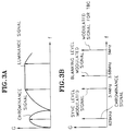
- Figures 3A and 3B show characteristics of the output frequency of the luminance/chrominance mixer 150 in the circuit shown in Figure 2, wherein Figure 3A is for frequency characteristics of the video signal in a horizontal scanning period and Figure 3B is for frequency characteristics of the video signal in a horizontal blanking interval.
- luminance/chrominance signal separator 100 separates video signals input through the input line 105 into a luminance signal and a chrominance signal and supplies the luminance signal to the input terminals of luminance signal modulator 110 and synchronizing signal separator 120 through the first output terminal and supplies the chrominance signal to the input terminal of chrominance signal modulator 111 through the second output terminal.
- the frequency of the luminance signal is frequency-modulated by a carrier signal so as to be recorded on a recording medium and the modulated luminance signal distributed in the same manner as the luminance signal of Figure 3A is supplied to the first selection point SP11 of the first controlling switch 144.
- chrominance signal modulator 111 the amplitude of a chrominance signal is modulated to be distributed in the frequency band of from 0 to 1.2 MHz in the same manner as the chrominance signal of Figure 3A and the low frequency converted chrominance signal is supplied to the second input terminal of luminance/chrominance signal mixer 150.
- Synchronizing signal separator 120 separates a horizontal synchronizing signal from the luminance signal to supply to the input terminals of the synchronizing level modulated signal generator 141, the blanking level modulated signal generator 142, the TBC reference signal generator 130 and the gate pulse generator 146.
- Reference signal generator 130 consists of a voltage controlled oscillator 43, a phase comparator 42 and a frequency divider 44 of a storing clock generator 40 as shown in Figure 1, detects the period variation of the horizontal synchronizing signal input from the synchronizing signal separator 120, and generates a TBC reference signal in the form of a clock pulse having a period varying in response to the period variation of the detected horizontal synchronizing signal.
- Waveform shaping circuit 131 filters the TBC reference signal in clock pulse form and generates a TBC reference signal waveform to a sine wave.
- Synchronizing level modulated signal generator 141 detects a synchronizing pulse from the horizontal synchronizing signals, applies a logic signal of a certain logic state (high or low logic state) to the control port CP2 of the second controlling switch 145 during detection of the synchronizing pulse, and supplies a synchronizing level modulated signal which is generated by frequency-modulating the detected synchronizing pulse by a carrier signal, to the first selection point SP21 of the second controlling switch 145.
- the synchronizing level modulated signal generator 141 can be composed of a level detector, an oscillator and a mixer to operate as described above, which are not shown in the drawing.
- Blanking level modulated signal generator 142 detects a blanking pulse from the horizontal synchronizing signals and supplies the blanking level modulated signal which is generated by frequency-modulating the detected blanking pulse level by a carrier signal, to the second selection point SP22 of the second controlling switch 145.
- the blanking level modulated signal generator 142 can be composed of a level detector, an oscillator and a mixer.
- the second controlling switch 145 operates when a logic signal is applied to the control port CP2 from the second output terminal of the synchronizing level modulated signal generator 141, and selects the output of the synchronizing level modulated signal generator 141, connected to the first selection point SP21 and supplies the result to the second input terminal of the reference signal mixer 143 during the synchronizing pulse duration of the horizontal synchronizing signal.
- the second controlling switch 145 selects the output of the blanking level modulated signal generator 142 connected to the second selection point SP22 and supplies the result to the second input terminal of the reference signal mixer 143 during the intervals other than the synchronizing pulse period duration of the horizontal synchronizing signal.
- the reference signal mixer 143 mixes the waveform-shaped TBC reference signal supplied from the waveform shaping circuit 131 with the modulated signals supplied from the reference connection point RP2 of the second controlling switch 145 and supplies the mixed signals to the second selection connection point SP12 of the first controlling switch 144.
- the frequencies of the signals are divided in the waveform shaping circuit 131 and are waveform to a sine waveform in order that the synchronizing level modulated signal is distributed around the zone of 3.4MHz, the blanking level modulated signal is distributed around the zone of 3.68MHz, and the TBC reference signal is distributed around the zone of 5MHz as shown in Figure 3B.
- the reason why the TBC reference signal is supplied to the first controlling switch 144 after being mixed with the blanking level modulated signal and synchronizing level modulated signal, is to prevent the appearance of the effects of higher harmonics and reflected waves on the output video signal by the noise included in the blanking interval and synchronizing period of the modulated luminance signal in which the TBC reference signal is to be inserted and by the insertion of the reference signal.
- gate pulse generator 146 In order to determine a region among the luminance signals in which the TBC reference signal is to be inserted, gate pulse generator 146 detects a synchronizing pulse or blanking pulse from the horizontal synchronizing signals, delays the detected synchronizing pulse or blanking pulse by a certain period (for instance, 55 ⁇ s ) shorter than the period of the horizontal synchronizing signal, generates a gate pulse having a width sufficient to cover the blanking interval of the horizontal synchronizing signal by the delayed pulse and supplies the gate pulse to the control port CP1 of the first controlling switch 144.
- a certain period for instance, 55 ⁇ s
- the first controlling switch 144 selects the output of the reference signal mixer 143 supplied to the second selection point SP12 while the gate pulse is applied from the gate pulse generator 146 to the control port CP1 and supplies the result to the first input terminal of the luminance/chrominance signal mixer 150.
- the first controlling switch 144 selects the output of the luminance signal modulator 110 supplied to the first selection point SP11 and supplies the selected output to the luminance/chrominance signal mixer 150.
- Luminance/chrominance signal mixer 150 mixes the modulated luminance signal, in which the TBC reference signal is inserted, supplied from the reference connection point RP1 of the first controlling switch 144 with the low frequency converted chrominance signal supplied from the chrominance signal modulator 111 and records the mixed signals on a recording medium through magnetic head 160.
- the video signal mixed in the luminance/chrominance mixer 150 has such frequency characteristic as shown in Figure 3A during a horizontal scanning period, and has such frequency characteristics as shown in Figure 3B during a blanking interval.
- the TBC reference signal recorded with the video signal is changed by the same amount of change as that occurring in the synchronizing signals. Accordingly, the video information of the video signal is time base corrected during reproducing by the changed TBC reference signal, thereby performing the correction precisely.
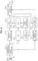
- FIG. 4 is a block diagram of an embodiment of a circuit for reproducing a TBC reference signal according to the present invention.
- magnetic head 300 is connected to the input terminal of luminance/chrominance signal separator 310.
- a first input terminal of the luminance/chrominance signal separator 310 is connected to input terminals of luminance signal demodulator 320 and band pass filter 351 and a second input terminal of the separator 310 is connected to an input terminal of chrominance signal demodulator 321.
- An output terminal of the luminance signal demodulator 320 is connected to an input terminal of a first TBC circuit 330.
- An output terminal of the first TBC circuit 330 is connected to an input terminal of synchronizing signal separator 361 and to a first input terminal of composite video signal generator 340.
- An output terminal of the band pass filter 351 is connected to an input terminal of burst injection locking circuit 360 (hereinafter referred to as BILC).
- An output terminal of BILC 360 is connected to control terminal of the first TBC circuit 330 and a second TBC circuit 331.
- An output terminal of synchronizing signal separator 361 is connected to an input terminal of gate pulse generator 362.
- the gate pulse generator 362 is connected to a control terminal of BILC 360.
- An output terminal of chrominance signal demodulator 321 is connected to an input terminal of the second TBC circuit 331.
- An output terminal of the second TBC circuit 331 is connected to a second input terminal of composite video signal generator 340.
- An output line terminal 305 of the composite video signal generator 340 is connected to an external display device or other video recording systems (not shown).
- magnetic head 300 reads out video information from a recording medium and supplies the information to luminance/chrominance signal separator 310.
- Luminance/chrominance signal separator 310 separates the video information supplied from the magnetic head 300 into a luminance signal mixed with a TBC reference signal and a chrominance signal.
- Luminance signal demodulator 320 frequency-demodulates the luminance signal mixed with the TBC reference signal and supplies the demodulated luminance signal to the first TBC circuit 330.
- Band pass filter 351 detects the TBC reference signal by band-pass filtering the luminance signal mixed with the TBC reference signal.
- BILC 360 When a gate pulse is applied to the control terminals, BILC 360 receives the TBC reference signal detected in the band pass filter 351 and regulates an output frequency according to the frequency of the input TBC reference signal. Then, the BILC 360 generates a clock pulse-shaped TBC reference signal having a regulated output frequency and supplies the generated signal to the control terminals of the first and second TBC circuits 330 and 331.
- the first TBC circuit 330 corrects the time base error of the demodulated luminance signal input from the luminance signal demodulator 320 by the TBC reference signal input from the BILC 360 and generates the corrected luminance signal.
- Synchronizing signal separator 361 separates a horizontal synchronizing signal from the corrected luminance signal and supplies the synchronizing signal to gate pulse generator 362.
- Gate pulse generator 362 which includes a delay device and a monostable multi-vibrator therein, delays a synchronizing pulse of a horizontal synchronizing signal until the next synchronizing pulse occurs by the delay device and generates, in the monostable multi-vibrator, a gate pulse having a width sufficient to cover the blanking interval of the horizontal synchronizing signal by the synchronizing pulse of the delayed horizontal synchronizing signal.
- the gate pulse is supplied to the control terminal of the BILC 360 to control the regulation of the output frequency of the BILC 360 during the blanking interval of the horizontal synchronizing signal.
- Chrominance signal demodulator 321 generates the demodulated chrominance signal by amplitude-demodulating the extracted chrominance signal.
- the second TBC circuit 331 corrects the time base error of the demodulated chrominance signal by the TBC reference signal to generate the corrected chrominance signal.
- Composite video signal generator 340 mixes the corrected luminance signal and the corrected chrominance signal to generate a composite video signal and supplies it to a display apparatus or other image recording systems through the output line 305.
- timing discordance of a video signal by a time base error during recording and reproducing operations can be adaptively corrected as the variation of synchronizing signals of a video signal occur by the TBC reference signal recorded together with the video signal.
Landscapes
- Engineering & Computer Science (AREA)
- Signal Processing (AREA)
- Multimedia (AREA)
- Television Signal Processing For Recording (AREA)
- Signal Processing Not Specific To The Method Of Recording And Reproducing (AREA)
Abstract
Description
- The present invention relates to a time base error corrector (TBC) for correcting timing discordance of video signals in video signal recording/reproducing systems, and more particularly to a circuit for recording and reproducing a reference signal used for correcting timing discordance of video signals.
- Generally, a video signal includes video information arranged in accordance with a synchronizing signal so as to display accurate images on display devices, and is affected by noise during recording and reproducing through a recording medium as are any other information signals, thereby producing time base errors in the video information. Time base errors occur mainly due to mechanical elements included in the recording/reproducing apparatus, which can tire viewers due to trembling of an image caused by the temporal lengthening or shortening of the signal.
- Especially when an analogue video signal is converted to a digital video signal for digitally processing the analogue video signal, a variation in the sampling number may occur due to the time base error, though the number of samples for each synchronization is required to be constant. As a result, video information designated for each pixel may move to the left or to the right by several pixels, so that the phase of the signal is not fixed and furthermore, signal processing between frames becomes impossible due to the changing pixel positions.
- A time base error corrector (hereinafter referred to as a TBC) is an apparatus that corrects the timing discordance of video information due to time base error of the video signal, and which is employed to remove the time base errors created during recording and reproducing and to resynchronize the signal more precisely in video recording and reproducing systems.
- A conventional TBC used in video recording and reproducing systems will be described below, referring to Figure 1 of the accompanying diagrammatic drawings.
- In Figure 1, analog to digital converter (A/D converter) 10 samples by a certain period and encodes a video signal entering through
input line 5, thereby generating a digital video signal. Memory 20 temporarily stores the digital video signal converted in the A/D converter 10. Digital to analog converter (D/A converter) 30 converts the digital video signal read-out from thememory 20 to an analog video signal and outputs it throughoutput line 15. To maintain uniformly the set number of samplings of A/D converter 10 and the number data stored inmemory 20 for every horizontal synchronization, storingclock generator 40 generates storing clocks having different periods according to the period variation of a horizontal synchronizing signal of a video signal supplied throughinput line 5 and supplies the storing clocks to A/D converter 10 andmemory 20.Reading clock generator 50 generates a reading clock having a certain period and supplies the clock tomemory 20 and D/A converter 30. In the storingclock generator 40 for generating storing clocks, synchronizingsignal separator 41 separates a horizontal synchronizing signal from a video signal supplied throughinput line 5 andphase comparator 42 compares the phase of the frequency-divided storing clock applied fromfrequency divider 44 with that of the horizontal synchronizing signal supplied from the synchronizingsignal separator 41 and generates a control voltage corresponding to the phase difference. Voltage controlled oscillator 43 (hereinafter referred to as VCO) generates storing clocks having different frequencies depending on the control voltages applied from thephase comparator 42 and supplies the clocks to A/D converter 10,memory 20 andfrequency divider 44. The frequency divider 44 frequency-divides the storing clocks in order that the clocks have the same frequency as that of the horizontal synchronizing signal and supplies the clocks tophase comparator 42. - Finally, the conventional TBC shown in Figure 1 samples a video signal by a certain number of samplings for each horizontal synchronizing period by regulating (adding/subtracting) the frequency of the storing clock according to the period variation of the horizontal synchronizing signal and stores the video signal into the memory. Then, such video data stored in the memory is read-out by the reading clock of a certain frequency and is converted to an analog video signal to correct the timing discordance of the video information of the video signals. However, in the case of the circuit shown in Figure 1, a negative feedback circuit is provided between the
phase comparator 42 and the VCO in order to regulate (add/subtract) the frequency of the storing clock for every horizontal synchronizing signal period. The time constant of the negative feedback circuit usually has a time period which is at least greater than the horizontal synchronizing signal period and usually of two or three times the horizontal synchronizing signal period. When the frequency transfer characteristic of a recording system is very narrow as compared with the band of an original signal, rise time and fall time of the horizontal synchronizing signal lengthens to make it difficult to locate a precise synchronizing position. Furthermore, due to the influence of noise and the like, the frequency of the storing clock cannot be changed precisely according to the variation of the horizontal synchronizing signal period. For these reasons, time base correction of a video signal can not be carried out precisely. - Preferred embodiments of the present invention aim to provide a circuit for recording and reproducing a TBC reference signal, in a video recording/reproducing system, which records a TBC reference signal with a video signal on a recording medium, and then corrects the time base errors of the video signal by the reproduced TBC reference signal so that precise time base error correction is attained.
- According to a first aspect of the present invention there is provided a circuit for recording/reproducing a TBC reference signal in video recording/reproducing systems including a recorder for recording a video signal on a recording medium and a reproducer for reproducing the video signal recorded on the recording medium and correcting the time base error, the circuit comprising:
adding means included in said recorder and used for adding a TBC reference signal to a video signal, said TBC reference signal having a period adaptively varying according to a synchronizing variation of the video signal to be recorded; and
means for extracting and reproducing said TBC reference signal from said video signal read-out from said recording medium in order to correct time base errors of said video signal reproduced on said reproducer. - Preferably, said TBC reference signal is added to a blanking interval of said video signal to be recorded.
- Preferably, said TBC reference signal is added, in the state in which it is mixed with signals in a blanking interval of a standard video signal instead of a signal in a blanking interval of said video signal to be recorded.
- According to a second aspect of the present invention there is provided a circuit for recording a TBC reference signal comprising:
means for modulating a video signal so as to be recorded on a recording medium;
means for generating a TBC reference signal having a period varying according to a synchronizing state of said video signal;
means for adding said TBC reference signal to a modulated video signal from said video signal modulating means; and
means for recording said modulated video signal to which a TBC reference signal is added by said reference signal adding means, on the recording medium. - Preferably, said reference signal adding means comprises a mixer for mixing said modulated video signal and TBC reference signal.
- Preferably, said reference signal adding means further comprises adding time control means for enabling said TBC reference signal to be added during a blanking interval of said modulated video signal.
- Preferably, said TBC reference signal is distributed in a frequency bandwidth sufficiently larger than that of signals in a blanking interval of said modulated video signal but smaller than that of the high cut-off frequency of said modulated video signal.
- Preferably, said reference signal adding means further comprises a standard modulated signal generating means for generating modulated signals for use as a standard in a blanking interval in order that the modulated signals can be inserted into the blanking interval of the modulated video signal together with said TBC reference signal instead of signals within the blanking interval of said modulated video signal to prevent external disturbances.
- According to a third aspect of the present invention there is provided a circuit for reproducing a TBC reference signal comprising:
means for reading out video information in which a TBC reference signal is inserted, from a recording medium;
means for demodulating said read-out video information to generate a video signal;
a TBC circuit for correcting time base errors of said demodulated video signal by said TBC reference signal;
means for separating a TBC reference signal from said read-out video signal; and
means for restoring said extracted TBC reference signal to supply said restored TBC reference signal to said TBC circuit. - Preferably, said reference signal extracting means comprises a band-pass filter.
- The invention extends to a video signal recording and/or reproducing apparatus provided with a circuit as above in accordance with any of the above aspects of the invention.
- Advantages of the present invention will be more apparent from the following description of preferred embodiments of the present invention, by way of example only, with reference to Figures 2 to 4 of the attached drawings, in which:
- Figure 2 is a block diagram of one example of a circuit for recording a reference signal for correcting time base error, according to one embodiment of the present invention;
- Figures 3A and 3B illustrate the frequency characteristics of a video signal processed by the circuit shown in Figure 2; and
- Figure 4 is a block circuit diagram of one example of an embodiment of the present invention for reproducing a reference signal for correcting time base error.
- Referring to Figure 2 wherein an embodiment of a circuit for recording a reference signal for correcting a time base error according to the present invention is shown,
input line 105 is connected to an external video signal source (not shown) and to the input terminal of luminance/chrominance signal separator 100. A first output terminal of the luminance/chrominance signal separator 100 is connected to input terminals of synchronizingsignal separator 120 andluminance signal modulator 110. A second output terminal of the luminance/chrominance signal separator 100 is connected to an input terminal ofchrominance signal modulator 111. An output terminal of theluminance signal modulator 110 is connected to a first selection point SP11 of a first controllingswitch 144. The reference connection point RP1 of the first controllingswitch 144 is connected to a first input terminal of luminance/chrominance signal mixer 150. An output terminal ofchrominance signal modulator 111 is connected to a second input terminal of luminance/chrominance signal mixer 150. An output terminal of luminance/chrominance signal mixer 150 is connected tomagnetic head 160. An output terminal of synchronizingsignal separator 120 is connected to input terminals of TBCreference signal generator 130, synchronizing level modulatedsignal generator 141, blanking level modulatedsignal generator 142 andgate pulse generator 146. An output terminal of TBCreference signal generator 130 is connected to an input terminal ofwaveform shaping circuit 131. An output terminal of thewaveform shaping circuit 131 is connected to a first input terminal ofreference signal mixer 143. A first output terminal of synchronizing level modulatedsignal generator 141 is connected to a first selection point SP21 of a second controllingswitch 145. A second output terminal of synchronizing level modulatedsignal generator 141 is connected to control port CP2 of the second controllingswitch 145. An output terminal of blanking level modulatedsignal generator 142 is connected to a second selection point SP22 of the second controllingswitch 145. An output terminal RP2 of the second controllingswitch 145 is connected to a second input terminal ofreference signal mixer 143. An output terminal of thereference signal mixer 143 is connected to a second selection point SP12 of the first controllingswitch 144. An output terminal ofgate pulse generator 146 is connected to control port CP1 of the first controllingswitch 144. - Figures 3A and 3B show characteristics of the output frequency of the luminance/
chrominance mixer 150 in the circuit shown in Figure 2, wherein Figure 3A is for frequency characteristics of the video signal in a horizontal scanning period and Figure 3B is for frequency characteristics of the video signal in a horizontal blanking interval. - In Figure 2, luminance/
chrominance signal separator 100 separates video signals input through theinput line 105 into a luminance signal and a chrominance signal and supplies the luminance signal to the input terminals ofluminance signal modulator 110 and synchronizingsignal separator 120 through the first output terminal and supplies the chrominance signal to the input terminal ofchrominance signal modulator 111 through the second output terminal. - In
luminance signal modulator 110, the frequency of the luminance signal is frequency-modulated by a carrier signal so as to be recorded on a recording medium and the modulated luminance signal distributed in the same manner as the luminance signal of Figure 3A is supplied to the first selection point SP11 of the firstcontrolling switch 144. - In
chrominance signal modulator 111, the amplitude of a chrominance signal is modulated to be distributed in the frequency band of from 0 to 1.2 MHz in the same manner as the chrominance signal of Figure 3A and the low frequency converted chrominance signal is supplied to the second input terminal of luminance/chrominance signal mixer 150. - Synchronizing
signal separator 120 separates a horizontal synchronizing signal from the luminance signal to supply to the input terminals of the synchronizing level modulatedsignal generator 141, the blanking level modulatedsignal generator 142, the TBCreference signal generator 130 and thegate pulse generator 146. -
Reference signal generator 130 consists of a voltage controlledoscillator 43, aphase comparator 42 and afrequency divider 44 of astoring clock generator 40 as shown in Figure 1, detects the period variation of the horizontal synchronizing signal input from the synchronizingsignal separator 120, and generates a TBC reference signal in the form of a clock pulse having a period varying in response to the period variation of the detected horizontal synchronizing signal. -
Waveform shaping circuit 131 filters the TBC reference signal in clock pulse form and generates a TBC reference signal waveform to a sine wave. - Synchronizing level modulated
signal generator 141 detects a synchronizing pulse from the horizontal synchronizing signals, applies a logic signal of a certain logic state (high or low logic state) to the control port CP2 of the secondcontrolling switch 145 during detection of the synchronizing pulse, and supplies a synchronizing level modulated signal which is generated by frequency-modulating the detected synchronizing pulse by a carrier signal, to the first selection point SP21 of the secondcontrolling switch 145. The synchronizing level modulatedsignal generator 141 can be composed of a level detector, an oscillator and a mixer to operate as described above, which are not shown in the drawing. - Blanking level modulated
signal generator 142 detects a blanking pulse from the horizontal synchronizing signals and supplies the blanking level modulated signal which is generated by frequency-modulating the detected blanking pulse level by a carrier signal, to the second selection point SP22 of the secondcontrolling switch 145. In order for the operation to take place, the blanking level modulatedsignal generator 142 can be composed of a level detector, an oscillator and a mixer. - The second
controlling switch 145 operates when a logic signal is applied to the control port CP2 from the second output terminal of the synchronizing level modulatedsignal generator 141, and selects the output of the synchronizing level modulatedsignal generator 141, connected to the first selection point SP21 and supplies the result to the second input terminal of thereference signal mixer 143 during the synchronizing pulse duration of the horizontal synchronizing signal. On the other hand, the secondcontrolling switch 145 selects the output of the blanking level modulatedsignal generator 142 connected to the second selection point SP22 and supplies the result to the second input terminal of thereference signal mixer 143 during the intervals other than the synchronizing pulse period duration of the horizontal synchronizing signal. - The
reference signal mixer 143 mixes the waveform-shaped TBC reference signal supplied from thewaveform shaping circuit 131 with the modulated signals supplied from the reference connection point RP2 of the secondcontrolling switch 145 and supplies the mixed signals to the second selection connection point SP12 of the firstcontrolling switch 144. - The frequencies of the signals are divided in the
waveform shaping circuit 131 and are waveform to a sine waveform in order that the synchronizing level modulated signal is distributed around the zone of 3.4MHz, the blanking level modulated signal is distributed around the zone of 3.68MHz, and the TBC reference signal is distributed around the zone of 5MHz as shown in Figure 3B. The reason why the TBC reference signal is supplied to the firstcontrolling switch 144 after being mixed with the blanking level modulated signal and synchronizing level modulated signal, is to prevent the appearance of the effects of higher harmonics and reflected waves on the output video signal by the noise included in the blanking interval and synchronizing period of the modulated luminance signal in which the TBC reference signal is to be inserted and by the insertion of the reference signal. - In order to determine a region among the luminance signals in which the TBC reference signal is to be inserted,
gate pulse generator 146 detects a synchronizing pulse or blanking pulse from the horizontal synchronizing signals, delays the detected synchronizing pulse or blanking pulse by a certain period (for instance, 55µs) shorter than the period of the horizontal synchronizing signal, generates a gate pulse having a width sufficient to cover the blanking interval of the horizontal synchronizing signal by the delayed pulse and supplies the gate pulse to the control port CP1 of the firstcontrolling switch 144. - The first
controlling switch 144 selects the output of thereference signal mixer 143 supplied to the second selection point SP12 while the gate pulse is applied from thegate pulse generator 146 to the control port CP1 and supplies the result to the first input terminal of the luminance/chrominance signal mixer 150. On the other hand, during the time that the gate pulse is not applied to the control port CP1, the firstcontrolling switch 144 selects the output of theluminance signal modulator 110 supplied to the first selection point SP11 and supplies the selected output to the luminance/chrominance signal mixer 150. - Luminance/
chrominance signal mixer 150 mixes the modulated luminance signal, in which the TBC reference signal is inserted, supplied from the reference connection point RP1 of the firstcontrolling switch 144 with the low frequency converted chrominance signal supplied from thechrominance signal modulator 111 and records the mixed signals on a recording medium throughmagnetic head 160. The video signal mixed in the luminance/chrominance mixer 150 has such frequency characteristic as shown in Figure 3A during a horizontal scanning period, and has such frequency characteristics as shown in Figure 3B during a blanking interval. - When the synchronizing signals of the video signal are changed by the effect of a time base error, the TBC reference signal recorded with the video signal is changed by the same amount of change as that occurring in the synchronizing signals. Accordingly, the video information of the video signal is time base corrected during reproducing by the changed TBC reference signal, thereby performing the correction precisely.
- Figure 4 is a block diagram of an embodiment of a circuit for reproducing a TBC reference signal according to the present invention. In Figure 4,
magnetic head 300 is connected to the input terminal of luminance/chrominance signal separator 310. A first input terminal of the luminance/chrominance signal separator 310 is connected to input terminals ofluminance signal demodulator 320 andband pass filter 351 and a second input terminal of theseparator 310 is connected to an input terminal ofchrominance signal demodulator 321. An output terminal of theluminance signal demodulator 320 is connected to an input terminal of afirst TBC circuit 330. An output terminal of thefirst TBC circuit 330 is connected to an input terminal of synchronizingsignal separator 361 and to a first input terminal of compositevideo signal generator 340. An output terminal of theband pass filter 351 is connected to an input terminal of burst injection locking circuit 360 (hereinafter referred to as BILC). An output terminal ofBILC 360 is connected to control terminal of thefirst TBC circuit 330 and asecond TBC circuit 331. An output terminal of synchronizingsignal separator 361 is connected to an input terminal ofgate pulse generator 362. Thegate pulse generator 362 is connected to a control terminal ofBILC 360. An output terminal ofchrominance signal demodulator 321 is connected to an input terminal of thesecond TBC circuit 331. An output terminal of thesecond TBC circuit 331 is connected to a second input terminal of compositevideo signal generator 340. - An
output line terminal 305 of the compositevideo signal generator 340 is connected to an external display device or other video recording systems (not shown). - In operation,
magnetic head 300 reads out video information from a recording medium and supplies the information to luminance/chrominance signal separator 310. - Luminance/
chrominance signal separator 310 separates the video information supplied from themagnetic head 300 into a luminance signal mixed with a TBC reference signal and a chrominance signal. -
Luminance signal demodulator 320 frequency-demodulates the luminance signal mixed with the TBC reference signal and supplies the demodulated luminance signal to thefirst TBC circuit 330. -
Band pass filter 351 detects the TBC reference signal by band-pass filtering the luminance signal mixed with the TBC reference signal. - When a gate pulse is applied to the control terminals,
BILC 360 receives the TBC reference signal detected in theband pass filter 351 and regulates an output frequency according to the frequency of the input TBC reference signal. Then, theBILC 360 generates a clock pulse-shaped TBC reference signal having a regulated output frequency and supplies the generated signal to the control terminals of the first andsecond TBC circuits - The
first TBC circuit 330 corrects the time base error of the demodulated luminance signal input from theluminance signal demodulator 320 by the TBC reference signal input from theBILC 360 and generates the corrected luminance signal. Synchronizingsignal separator 361 separates a horizontal synchronizing signal from the corrected luminance signal and supplies the synchronizing signal togate pulse generator 362. -
Gate pulse generator 362, which includes a delay device and a monostable multi-vibrator therein, delays a synchronizing pulse of a horizontal synchronizing signal until the next synchronizing pulse occurs by the delay device and generates, in the monostable multi-vibrator, a gate pulse having a width sufficient to cover the blanking interval of the horizontal synchronizing signal by the synchronizing pulse of the delayed horizontal synchronizing signal. The gate pulse is supplied to the control terminal of theBILC 360 to control the regulation of the output frequency of theBILC 360 during the blanking interval of the horizontal synchronizing signal. -
Chrominance signal demodulator 321 generates the demodulated chrominance signal by amplitude-demodulating the extracted chrominance signal. - The
second TBC circuit 331 corrects the time base error of the demodulated chrominance signal by the TBC reference signal to generate the corrected chrominance signal. - Composite
video signal generator 340 mixes the corrected luminance signal and the corrected chrominance signal to generate a composite video signal and supplies it to a display apparatus or other image recording systems through theoutput line 305. - The embodiments of the present invention that are described in detail above are advantageous in that, in systems for recording and reproducing a video signal, timing discordance of a video signal by a time base error during recording and reproducing operations can be adaptively corrected as the variation of synchronizing signals of a video signal occur by the TBC reference signal recorded together with the video signal.
- The reader's attention is directed to all papers and documents which are filed concurrently with or previous to this specification in connection with this application and which are open to public inspection with this specification, and the contents of all such papers and documents are incorporated herein by reference.
- All of the features disclosed in this specification (including any accompanying claims, abstract and drawings), and/or all of the steps of any method or process so disclosed, may be combined in any combination, except combinations where at least some of such features and/or steps are mutually exclusive.
- Each feature disclosed in this specification (including any accompanying claims, abstract and drawings), may be replaced by alternative features serving the same, equivalent or similar purpose, unless expressly stated otherwise. Thus, unless expressly stated otherwise, each feature disclosed is one example only of a generic series of equivalent or similar features.
- The invention is not restricted to the details of the foregoing embodiment(s). The invention extends to any novel one, or any novel combination, of the features disclosed in this specification (including any accompanying claims, abstract and drawings), or to any novel one, or any novel combination, of the steps of any method or process so disclosed.
Claims (11)
- A circuit for recording/reproducing a TBC reference signal in video recording/reproducing systems including a recorder for recording a video signal on a recording medium and a reproducer for reproducing the video signal recorded on the recording medium and correcting the time base error, the circuit comprising:
adding means included in said recorder and used for adding a TBC reference signal to a video signal, said TBC reference signal having a period adaptively varying according to a synchronizing variation of the video signal to be recorded; and
means for extracting and reproducing said TBC reference signal from said video signal read-out from said recording medium in order to correct time base errors of said video signal reproduced on said reproducer. - A circuit for recording/reproducing a TBC reference signal as claimed in claim 1, wherein said TBC reference signal is added to a blanking interval of said video signal to be recorded.
- A circuit for recording/reproducing a TBC reference signal as claimed in claim 2, wherein said TBC reference signal is added, in the state in which it is mixed with signals in a blanking interval of a standard video signal instead of a signal in a blanking interval of said video signal to be recorded.
- A circuit for recording a TBC reference signal comprising:
means for modulating a video signal so as to be recorded on a recording medium;
means for generating a TBC reference signal having a period varying according to a synchronizing state of said video signal;
means for adding said TBC reference signal to a modulated video signal from said video signal modulating means; and
means for recording said modulated video signal to which a TBC reference signal is added by said reference signal adding means, on the recording medium. - A circuit for recording a TBC reference signal as claimed in claim 4, wherein said reference signal adding means comprises a mixer for mixing said modulated video signal and TBC reference signal.
- A circuit for recording a TBC reference signal as claimed in claim 5, wherein said reference signal adding means further comprises adding time control means for enabling said TBC reference signal to be added during a blanking interval of said modulated video signal.
- A circuit for recording a TBC reference signal as claimed in claim 6, wherein said TBC reference signal is distributed in a frequency bandwidth sufficiently larger than that of signals in a blanking interval of said modulated video signal but smaller than that of the high cut-off frequency of said modulated video signal.
- A circuit for recording a TBC reference signal as claimed in claim 6 or 7, wherein said reference signal adding means further comprises a standard modulated signal generating means for generating modulated signals for use as a standard in a blanking interval in order that the modulated signals can be inserted into the blanking interval of the modulated video signal together with said TBC reference signal instead of signals within the blanking interval of said modulated video signal to prevent external disturbances.
- A circuit for reproducing a TBC reference signal comprising:
means for reading out video information in which a TBC reference signal is inserted, from a recording medium;
means for demodulating said read-out video information to generate a video signal;
a TBC circuit for correcting time base errors of said demodulated video signal by said TBC reference signal;
means for separating a TBC reference signal from said read-out video signal; and
means for restoring said extracted TBC reference signal to supply said restored TBC reference signal to said TBC circuit. - A circuit for reproducing a TBC reference signal as claimed in claim 9, wherein said reference signal extracting means comprises a band-pass filter.
- A video signal recording and/or reproducing apparatus provided with a circuit according to any of the preceding claims.
Applications Claiming Priority (2)
| Application Number | Priority Date | Filing Date | Title |
|---|---|---|---|
| KR1019900018736A KR930004219B1 (en) | 1990-11-19 | 1990-11-19 | Time base error correction standard signal recording and reproducing circuit |
| KR1873690 | 1990-11-19 |
Publications (3)
| Publication Number | Publication Date |
|---|---|
| EP0487184A2 true EP0487184A2 (en) | 1992-05-27 |
| EP0487184A3 EP0487184A3 (en) | 1993-03-17 |
| EP0487184B1 EP0487184B1 (en) | 1997-06-11 |
Family
ID=19306202
Family Applications (1)
| Application Number | Title | Priority Date | Filing Date |
|---|---|---|---|
| EP91306616A Expired - Lifetime EP0487184B1 (en) | 1990-11-19 | 1991-07-19 | Circuit for recording and reproducing time base error corrector reference signal |
Country Status (9)
| Country | Link |
|---|---|
| EP (1) | EP0487184B1 (en) |
| JP (1) | JP3056555B2 (en) |
| KR (1) | KR930004219B1 (en) |
| CN (1) | CN1033781C (en) |
| CA (1) | CA2050119C (en) |
| DE (1) | DE69126505T2 (en) |
| ES (1) | ES2104670T3 (en) |
| MY (1) | MY111952A (en) |
| RU (1) | RU2072565C1 (en) |
Cited By (1)
| Publication number | Priority date | Publication date | Assignee | Title |
|---|---|---|---|---|
| DE4329841C2 (en) * | 1992-09-04 | 2003-05-22 | Pentax Corp | Device for recording and playing back a video signal |
Families Citing this family (1)
| Publication number | Priority date | Publication date | Assignee | Title |
|---|---|---|---|---|
| US5899578A (en) * | 1995-12-25 | 1999-05-04 | Sony Corporation | Digital signal processor, processing method, digital signal recording/playback device and digital signal playback method |
Citations (5)
| Publication number | Priority date | Publication date | Assignee | Title |
|---|---|---|---|---|
| US4672470A (en) * | 1983-12-27 | 1987-06-09 | Matsushita Electric Industrial Co., Ltd. | Video signal recording and reproducing apparatus |
| US4688081A (en) * | 1985-01-25 | 1987-08-18 | Hitachi, Ltd. | Apparatus for correcting time base error of video signal |
| EP0265085A2 (en) * | 1986-09-25 | 1988-04-27 | Pioneer Electronic Corporation | Digitally-recorded disk playing device |
| DE3909847A1 (en) * | 1989-03-25 | 1990-09-27 | Broadcast Television Syst | Method and circuit arrangement for generating an auxiliary signal |
| EP0475750A1 (en) * | 1990-09-14 | 1992-03-18 | Matsushita Electric Industrial Co., Ltd. | Video tape recorder |
Family Cites Families (1)
| Publication number | Priority date | Publication date | Assignee | Title |
|---|---|---|---|---|
| JPS62265876A (en) * | 1986-05-13 | 1987-11-18 | Mitsubishi Electric Corp | Time base correcting device for video signal recording and reproducing device |
-
1990
- 1990-11-19 KR KR1019900018736A patent/KR930004219B1/en not_active IP Right Cessation
-
1991
- 1991-07-19 EP EP91306616A patent/EP0487184B1/en not_active Expired - Lifetime
- 1991-07-19 DE DE69126505T patent/DE69126505T2/en not_active Expired - Fee Related
- 1991-07-19 ES ES91306616T patent/ES2104670T3/en not_active Expired - Lifetime
- 1991-08-28 CA CA002050119A patent/CA2050119C/en not_active Expired - Fee Related
- 1991-08-30 MY MYPI91001581A patent/MY111952A/en unknown
- 1991-09-24 CN CN91109362A patent/CN1033781C/en not_active Expired - Fee Related
- 1991-09-24 JP JP3243006A patent/JP3056555B2/en not_active Expired - Fee Related
- 1991-09-25 RU SU915001609A patent/RU2072565C1/en not_active IP Right Cessation
Patent Citations (5)
| Publication number | Priority date | Publication date | Assignee | Title |
|---|---|---|---|---|
| US4672470A (en) * | 1983-12-27 | 1987-06-09 | Matsushita Electric Industrial Co., Ltd. | Video signal recording and reproducing apparatus |
| US4688081A (en) * | 1985-01-25 | 1987-08-18 | Hitachi, Ltd. | Apparatus for correcting time base error of video signal |
| EP0265085A2 (en) * | 1986-09-25 | 1988-04-27 | Pioneer Electronic Corporation | Digitally-recorded disk playing device |
| DE3909847A1 (en) * | 1989-03-25 | 1990-09-27 | Broadcast Television Syst | Method and circuit arrangement for generating an auxiliary signal |
| EP0475750A1 (en) * | 1990-09-14 | 1992-03-18 | Matsushita Electric Industrial Co., Ltd. | Video tape recorder |
Non-Patent Citations (2)
| Title |
|---|
| IEEE TRANSACTIONS ON CONSUMER ELECTRONICS vol. CE-32, no. 3, May 1986, NEW YORK US pages 107 - 114 FURUHATA ET AL 'A HIGH-DEFINITION MUSE VCR WITH ANALOG SEGMENT RECORDING METHOD' * |
| INTERNATIONAL BROADCASTING CONVENTION September 1988, BRIGHTON, GB pages 414 - 417 SCHIFFLER ET AL 'AN HDTV VTR: ANALOG RECORDING WITH DIGITAL SIGNAL PROCESSING' * |
Cited By (1)
| Publication number | Priority date | Publication date | Assignee | Title |
|---|---|---|---|---|
| DE4329841C2 (en) * | 1992-09-04 | 2003-05-22 | Pentax Corp | Device for recording and playing back a video signal |
Also Published As
| Publication number | Publication date |
|---|---|
| CA2050119C (en) | 1997-12-16 |
| KR930004219B1 (en) | 1993-05-21 |
| DE69126505T2 (en) | 1998-01-22 |
| RU2072565C1 (en) | 1997-01-27 |
| CN1033781C (en) | 1997-01-08 |
| KR920010593A (en) | 1992-06-26 |
| MY111952A (en) | 2001-03-31 |
| ES2104670T3 (en) | 1997-10-16 |
| JPH04286483A (en) | 1992-10-12 |
| EP0487184B1 (en) | 1997-06-11 |
| EP0487184A3 (en) | 1993-03-17 |
| DE69126505D1 (en) | 1997-07-17 |
| JP3056555B2 (en) | 2000-06-26 |
| CN1061690A (en) | 1992-06-03 |
| CA2050119A1 (en) | 1992-05-20 |
Similar Documents
| Publication | Publication Date | Title |
|---|---|---|
| US5245430A (en) | Timebase corrector with drop-out compensation | |
| US4825299A (en) | Magnetic recording/reproducing apparatus utilizing phase comparator | |
| US4438456A (en) | Time base corrector | |
| JPS60140993A (en) | Recording/reproducing device | |
| CA1326900C (en) | Jitter detecting apparatus for detecting a vtr recording/reproducing video signal | |
| US5526129A (en) | Time-base-correction in video recording using a frequency-modulated carrier | |
| US5191434A (en) | Synchronizing signal restoration circuit | |
| JPH0712229B2 (en) | Time axis correction device | |
| EP0487184B1 (en) | Circuit for recording and reproducing time base error corrector reference signal | |
| US5923377A (en) | Jitter reducing circuit | |
| US5319467A (en) | Video tape recorder for recording a video signal with an additional time-base reference signal | |
| US5200833A (en) | Signal level clamping apparatus for a CTDM video signal | |
| US5594553A (en) | Video signal recording and reproducing apparatus using signal modification to remove jitter | |
| JPS60100893A (en) | Time sequential transmission system | |
| US5598274A (en) | Image signal recording and reproducing system | |
| US5206768A (en) | Method and apparatus for writing video signal in memory | |
| JPH0752962B2 (en) | Color video signal recording / playback method | |
| KR100236134B1 (en) | Timebase corrector with drop-out compensation | |
| JPS61228787A (en) | Recording method for video signal | |
| JPH0686230A (en) | Video signal recording and reproducing device | |
| JPS5833379A (en) | Static picture recorder | |
| JPH0681333B2 (en) | Video signal processor | |
| JPS6236431B2 (en) | ||
| JPH01220996A (en) | High speed phase matching circuit | |
| JPH03154495A (en) | Picture signal recording and reproducing system |
Legal Events
| Date | Code | Title | Description |
|---|---|---|---|
| PUAI | Public reference made under article 153(3) epc to a published international application that has entered the european phase |
Free format text: ORIGINAL CODE: 0009012 |
|
| AK | Designated contracting states |
Kind code of ref document: A2 Designated state(s): DE ES GB NL |
|
| PUAL | Search report despatched |
Free format text: ORIGINAL CODE: 0009013 |
|
| AK | Designated contracting states |
Kind code of ref document: A3 Designated state(s): DE ES GB NL |
|
| 17P | Request for examination filed |
Effective date: 19930908 |
|
| 17Q | First examination report despatched |
Effective date: 19950131 |
|
| GRAG | Despatch of communication of intention to grant |
Free format text: ORIGINAL CODE: EPIDOS AGRA |
|
| GRAH | Despatch of communication of intention to grant a patent |
Free format text: ORIGINAL CODE: EPIDOS IGRA |
|
| GRAH | Despatch of communication of intention to grant a patent |
Free format text: ORIGINAL CODE: EPIDOS IGRA |
|
| GRAA | (expected) grant |
Free format text: ORIGINAL CODE: 0009210 |
|
| AK | Designated contracting states |
Kind code of ref document: B1 Designated state(s): DE ES GB NL |
|
| REF | Corresponds to: |
Ref document number: 69126505 Country of ref document: DE Date of ref document: 19970717 |
|
| REG | Reference to a national code |
Ref country code: ES Ref legal event code: FG2A Ref document number: 2104670 Country of ref document: ES Kind code of ref document: T3 |
|
| PLBE | No opposition filed within time limit |
Free format text: ORIGINAL CODE: 0009261 |
|
| STAA | Information on the status of an ep patent application or granted ep patent |
Free format text: STATUS: NO OPPOSITION FILED WITHIN TIME LIMIT |
|
| 26N | No opposition filed | ||
| REG | Reference to a national code |
Ref country code: GB Ref legal event code: IF02 |
|
| PGFP | Annual fee paid to national office [announced via postgrant information from national office to epo] |
Ref country code: ES Payment date: 20080821 Year of fee payment: 18 Ref country code: DE Payment date: 20080724 Year of fee payment: 18 |
|
| PGFP | Annual fee paid to national office [announced via postgrant information from national office to epo] |
Ref country code: NL Payment date: 20080703 Year of fee payment: 18 |
|
| PGFP | Annual fee paid to national office [announced via postgrant information from national office to epo] |
Ref country code: GB Payment date: 20080723 Year of fee payment: 18 |
|
| GBPC | Gb: european patent ceased through non-payment of renewal fee |
Effective date: 20090719 |
|
| NLV4 | Nl: lapsed or anulled due to non-payment of the annual fee |
Effective date: 20100201 |
|
| PG25 | Lapsed in a contracting state [announced via postgrant information from national office to epo] |
Ref country code: GB Free format text: LAPSE BECAUSE OF NON-PAYMENT OF DUE FEES Effective date: 20090719 |
|
| PG25 | Lapsed in a contracting state [announced via postgrant information from national office to epo] |
Ref country code: DE Free format text: LAPSE BECAUSE OF NON-PAYMENT OF DUE FEES Effective date: 20100202 |
|
| REG | Reference to a national code |
Ref country code: ES Ref legal event code: FD2A Effective date: 20090720 |
|
| PG25 | Lapsed in a contracting state [announced via postgrant information from national office to epo] |
Ref country code: ES Free format text: LAPSE BECAUSE OF NON-PAYMENT OF DUE FEES Effective date: 20090720 |
|
| PG25 | Lapsed in a contracting state [announced via postgrant information from national office to epo] |
Ref country code: NL Free format text: LAPSE BECAUSE OF NON-PAYMENT OF DUE FEES Effective date: 20100201 |