EP0486101A2 - Circuit numérique pour réaliser approximativement une modulation GMSK (Gaussian minimum shift keying) - Google Patents
Circuit numérique pour réaliser approximativement une modulation GMSK (Gaussian minimum shift keying) Download PDFInfo
- Publication number
- EP0486101A2 EP0486101A2 EP91202930A EP91202930A EP0486101A2 EP 0486101 A2 EP0486101 A2 EP 0486101A2 EP 91202930 A EP91202930 A EP 91202930A EP 91202930 A EP91202930 A EP 91202930A EP 0486101 A2 EP0486101 A2 EP 0486101A2
- Authority
- EP
- European Patent Office
- Prior art keywords
- values
- filter
- phase generator
- registers
- output
- Prior art date
- Legal status (The legal status is an assumption and is not a legal conclusion. Google has not performed a legal analysis and makes no representation as to the accuracy of the status listed.)
- Withdrawn
Links
- 230000015654 memory Effects 0.000 claims description 74
- 230000015572 biosynthetic process Effects 0.000 claims description 6
- 230000006870 function Effects 0.000 description 14
- 238000000034 method Methods 0.000 description 6
- 238000011161 development Methods 0.000 description 2
- 230000014509 gene expression Effects 0.000 description 2
- 230000003595 spectral effect Effects 0.000 description 2
- 230000005540 biological transmission Effects 0.000 description 1
- 238000004364 calculation method Methods 0.000 description 1
- 238000005314 correlation function Methods 0.000 description 1
- 230000001934 delay Effects 0.000 description 1
- 238000013461 design Methods 0.000 description 1
- 230000010354 integration Effects 0.000 description 1
- 238000010295 mobile communication Methods 0.000 description 1
- 238000005070 sampling Methods 0.000 description 1
- 238000001228 spectrum Methods 0.000 description 1
- 238000012546 transfer Methods 0.000 description 1
Images

Classifications
-
- H—ELECTRICITY
- H03—ELECTRONIC CIRCUITRY
- H03M—CODING; DECODING; CODE CONVERSION IN GENERAL
- H03M7/00—Conversion of a code where information is represented by a given sequence or number of digits to a code where the same, similar or subset of information is represented by a different sequence or number of digits
-
- H—ELECTRICITY
- H04—ELECTRIC COMMUNICATION TECHNIQUE
- H04L—TRANSMISSION OF DIGITAL INFORMATION, e.g. TELEGRAPHIC COMMUNICATION
- H04L27/00—Modulated-carrier systems
- H04L27/18—Phase-modulated carrier systems, i.e. using phase-shift keying
- H04L27/20—Modulator circuits; Transmitter circuits
- H04L27/2003—Modulator circuits; Transmitter circuits for continuous phase modulation
- H04L27/2007—Modulator circuits; Transmitter circuits for continuous phase modulation in which the phase change within each symbol period is constrained
- H04L27/2017—Modulator circuits; Transmitter circuits for continuous phase modulation in which the phase change within each symbol period is constrained in which the phase changes are non-linear, e.g. generalized and Gaussian minimum shift keying, tamed frequency modulation
Definitions
- the invention relates to a digital circuit arrangement for the approximate realization of a GMSK (Gaussian Mininum Shift Keying) modulation, which contains a linear filter arrangement for generating a sequence of imaginary and a sequence of real output values from a sequence of binary input values.
- GMSK Gausian Mininum Shift Keying
- the digital data to be transmitted are modulated and transmitted as an analog signal in a radio high-frequency channel.
- GMSK Gausian Minimum Shift Keying
- Such a GMSK modulator modulates a stream of binary input values a k , each of which corresponds to one bit.
- the character ⁇ describes a modulo-2 addition
- the character * is the convolution symbol
- T B describes the time period between two successive input values a k and ⁇ 0 is the carrier frequency.
- the aforementioned circuit arrangement for GMSK modulation which generates an output signal y (t), is known from EP-A2-0 371 751.
- the known circuit arrangement contains two memory circuits.
- the address inputs of each memory circuit are connected to three registers and an interpolation counter.
- the interpolation counter supplies each memory circuit with a clock signal with an increased frequency compared to the frequency of the clock signal with which the input values are read into a first memory.
- the input circuits are supplied to the memory circuits from the first register, the phase values of the input values from a second register and values for synchronization from a third register.
- a non-recursive filter, an integration, a calculation of sine and cosine values for the generation of imaginary and real ones is made by the memory circuits
- Output values and a non-return zero (NRZ) coding are simulated. This essentially calculates the output signal y (t) specified above.
- the real and imaginary output values are each fed to a digital-to-analog converter and a subsequent low-pass filter.
- the invention has for its object to provide a circuit arrangement for GMSK modulation, which has a lower implementation cost.
- phase generator is provided as a binary-coded phase generator value as a function of two successive binary input values for outputting the real numbers 1 or -1 or the imaginary numbers j or -j, that the phase generator if two consecutive input values for changing the numbers are in positive order from 1 to j or from j to -1 or from -1 to -j or from -j to 1 and if two consecutive input values are inequality to change the numbers is provided in reverse negative order and that the linear filter arrangement is provided for receiving the phase generator values and for generating the real and imaginary output values.
- the function x1 (t) represents the carrier signal mentioned above. After multiplying the function y (t) by the carrier signal x1 (t), the modulated output signal results.
- the phase generator which outputs the real numbers 1 or -1 and the imaginary numbers j and -j, represents the time-discrete implementation of the function s0 (t). If two successive input values are the same, the phase generator outputs phase generator values that differ from 1 change to j or from j to -1 or from -1 to -j or from -j to 1. If there are two consecutive unequal input values, the phase generator value changes from j to 1 or from 1 to -j or from -j to -1 or from -1 to j.
- This linear filter arrangement can consist of two recursive or non-recursive filters. One filter forms the imaginary and the other filter the real output value.
- the coefficients h l of the filters can be determined using various methods. In a first method, the linear filter arrangement is optimized according to regulations in the frequency and time domain. In a second method, the cross-correlation function between the function (1) and the sequence of the input values a k is determined for a quasi-random sequence. The coefficients of the filter arrangement are calculated on this basis.
- the linear filter arrangement must therefore be designed so that its output time function approximately results in the output time function, which can be calculated from function (1).
- Such a filter arrangement has a bell-shaped transfer function.
- the phase generator alternately supplies imaginary and real phase generator values. It is therefore only essential that the linear filter arrangement receive sign information. The phase generator thus only supplies the linear filter arrangement with the sign bit as the phase generator value.
- the linear filter arrangement designed as a non-recursive filter contains a chain of registers which are provided for running through the phase generator values to be supplied by the phase generator. that a combination circuit contained in the filter is provided for generating two filter values each from the phase generator value to be supplied by the phase generator and the output values of the registers, that the combination circuit for forming a first filter value by a first weighting of the phase generator value and the output values of the registers, which for Obtaining a value running through the chain after passing through each of (2n + 1) registers, where n is a natural number, and by summing the first weighted values and to form a second filter value by a second weighting of the other output values and by summing the second weighted values is provided and that a switch arrangement contained in the filter for supplying the two filter values and after each filter value formation is alternately provided for outputting the filter values as real or imaginary output values.
- multipliers each assigned to the input of the first register of the chain of registers and to each output of the registers, which are set up to multiply the phase generator value and the output values of the registers by coefficients, form a first adder for formation contains the first filter value by summing the first weighted values and a second adder to form the second filter value by summing the second weighted values.
- the weighting with coefficients is realized with multipliers. After the multiplication, the filter values are formed by adding the multiplied values.
- the real and imaginary output values must each pass through a digital-to-analog converter and a low-pass filter before being modulated after multiplication with the carrier signal in an analog multiplier Output signal can be given over a radio transmission link. Every analog low pass suppresses disturbing, mirrored spectral components. So that such an analog low-pass filter can be carried out in a simple manner, further filter values are formed between one clock interval of the registers (oversampling). This results in an expansion of the spectrum, so that the low-pass filter can be designed so that it can have a flatter edge at the cutoff frequency. This can be achieved in that the multipliers are provided several times during a clock interval of the registers for multiplying the phase generator value and the output values of the registers with different coefficients to form oversampled first and second filter values.
- the combination circuit contains a first control circuit, a first coefficient memory and an accumulator, that the first control circuit is provided one after the other in time for supplying the phase generator value and the output values of the registers as addresses for the first coefficient memory for supplying coefficients to the accumulator and that the accumulator is successively provided for receiving coefficients and the corresponding sign bit supplied by the first control circuit and for forming the first and second filter values.
- the accumulator is supplied with a coefficient from the first coefficient memory in succession. First the first filter value and then the second filter value is calculated.
- oversampling can also be implemented. This can be realized by the first control circuit during a Clock intervals of the registers are provided several times in succession for supplying the phase generator value, the output values of the registers and from a pointer address to the first coefficient memory, that the pointer address is used to output how often the phase generator value and the output values of the register have been used as addresses during the clock interval, and that the accumulator is provided for forming oversampled first and second filter values from the coefficients.
- the combination circuit contains a second control circuit and a second and third coefficient memory, that the second control circuit for supplying the phase generator value and the output values of the registers which serve to form the first filter value are provided as addresses for the second coefficient memory is that the second coefficient memory is provided for outputting the first filter value, that the second control circuit for supplying the output values of the registers, which serve to form the second filter value, is provided as an address for the third coefficient memory, and that the third coefficient memory is provided for outputting the second filter value. All possible results for the first and second filter values are stored in the two coefficient memories.
- the second control circuit calls the result at the output of the coefficient memory by applying an address to the coefficient memory.
- oversampled first and second filter values can also be formed.
- the second control circuit is provided several times in succession during a clock interval for feeding the phase generator value, output values of registers and a pointer address to the second coefficient memory and for feeding output values of registers and the pointer address to the third coefficient memory, that the pointer address is used for outputting how often the phase generator value and the output values of the registers have been used as addresses during the clock interval, and that the second and third coefficient memories are provided for outputting oversampled first and second filter values.
- an EXCLUSIVE-OR gate is provided for receiving the input values and values from an input register, that the input register is provided for receiving the input values, and that a counter is provided for receiving the output signal of the EXCLUSIVE-OR gate at its counting direction input and for delivering the phase generator values to its counter output.
- the circuit arrangement shown in Fig. 1 for the approximate realization of GMSK modulation contains a phase generator 1 and a linear filter arrangement 2.
- the phase generator 1 comprises an EXCLUSIVE-OR gate 3, an input register 4 and a counter 5.
- the EXCLUSIVE-OR gate 3 and the input register 4 receive binary input values, each consisting of one bit.
- the output of the input register 4 is connected to a further input of the EXCLUSIVE-OR gate 3.
- the output of the EXCLUSIVE-OR gate 3 is connected to a counting direction input of the counter 5.
- the counter 5 represents an up-down 2-bit counter.
- the 2-bit values which the counter 5 outputs at its output are intended to represent the real numbers 1 or -1 or the imaginary numbers j or -j.
- One output of the counter 5 indicates the sign bit and the other output, whether the number is real or imaginary. If two consecutive binary input values are the same, the number at the output of phase generator 1 changes from j to -1 or from -1 to -j or from -j to 1 or from 1 to j. If two consecutive binary input values are different, the number at the output of phase generator 1 changes from j to 1 or from 1 to -j or from -j to -1 or from -1 to j.
- the linear filter arrangement 2 arranged subsequently is supplied as phase generator value by the phase generator 1 only the sign bit, since the other bit at the output of the counter 5 contains no information.
- the linear filter arrangement 2 is realized by a non-recursive filter, the coefficients of which can be determined according to one of the design methods specified above.
- the linear filter arrangement 2, the input register 4 and the counter 5 still receive a clock signal T1. Furthermore, the linear filter arrangement 2 receives a clock signal T2, the frequency of which is greater by a factor of 8 than the frequency of the clock signal T1.
- the linear filter arrangement 2 has two outputs 6 and 7.
- the output 6 provides a sequence of imaginary and the output 7 a sequence of real output values.
- oversampling is realized by a factor of 8, ie eight imaginary and eight real output values result for a phase value.
- the output 6 of the linear filter arrangement 2 is connected to a digital-to-analog converter 8 and the output 7 to a further digital-to-analog converter 9.
- Both digital-to-analog converter 8 and 9 receive the clock signal T2.
- the output of each digital-to-analog converter 8 and 9 is connected to a low-pass filter 10 and 11.
- the output of the low pass 10 is connected to a multiplier 54 which multiplies the analog output signal of the low pass 10 by a sine signal.
- the output signal of the low-pass filter 11 is also multiplied by a sine signal, but offset by 90 ° with respect to the former Multiplied by 55.
- the two output signals of multipliers 54 and 55 are combined in an adder 56 and form the modulated output signal of the modulator.
- FIG. 2 A first exemplary embodiment of the linear filter arrangement 2 is shown in FIG. 2.
- the phase values supplied by the counter 5 are fed to a chain of four registers 12 to 15.
- Each of the registers 12 to 15 delays a signal supplied to it by one clock of the clock signal T 1.
- the registers 12 to 15 also receive the clock signal T1.
- the sequence of the phase generator values and the sequence of the output values of the registers 12 to 15 are fed to a combination circuit 16.
- the combination circuit 16 contains five multipliers 17 to 21, partial coefficient memories 22 to 26 assigned to the multipliers 17 to 21, a first adder 27 and a second adder 28.
- the sequence of the phase generator values is obtained by the multiplier 17, the coefficient supplied by the partial coefficient memory 22 will.
- the multipliers 18 to 21 are each supplied with coefficients from the partial coefficient memories 23 to 26.
- the sequence of the output values of the register 12 are supplied to the multiplier 18, the sequence of the output values of the register 13 to the multiplier 19, the sequence of the output values of the register 14 to the multiplier 20 and the sequence of the output values of the register 15 to the multiplier 21.
- each phase generator value and each output value of the registers 12 to 15 are successively multiplied by eight coefficients. In this way, oversampling is realized by a factor of 8.
- each partial coefficient memory 22 to 26 also contains a control part. The following Coefficients are stored in the partial coefficient memories 22 to 26:
- the coefficients h1 to h8 in the partial coefficient memory 23 the coefficients h9 to h16, in the partial coefficient memory 24 the coefficients h17 to h24, in the partial coefficient memory 25 the coefficients h25 to h32 and in the coefficients h33 to h40 are stored in the partial coefficient memory 26.
- the first adder 27 contains the phase generator values weighted with the coefficients of the partial coefficient memory 16, and those with the coefficients of the partial coefficient memory 16 24 weighted output values of the register 13 and the output values of the register 15 weighted with the coefficients of the partial coefficient memory 26 are added.
- the output values of the register 12 weighted with the coefficients of the partial coefficient memory 23 and the output values of the register 14 weighted with the coefficients of the partial coefficient memory 25 are added in the second adder 28.
- the first filter value formed by the first adder 27 and the second filter value formed by the second adder 28 are fed to a switch arrangement 29 which contains a first switch 30 and a second switch 33.
- the first switch 30 connects the output of the first adder 27 or the output of the second adder 28 to its output 32.
- the second switch 33 also connects the output of the first adder 27 or the output of the second adder 28 to its output 31.
- the two switches are switched in opposite directions. When the output 32 of the first switch 30 is connected to the output of the first adder 27, the output 31 of the second switch 33 is connected to the output of the second adder 28 and vice versa.
- multipliers 17 to 21, the partial coefficient memories 22 to 26, the first adder 27, the second adder 28 and the switches 30 and 33 are supplied with the clock signal T 1.
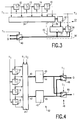
- FIG. 3 Another embodiment of the linear filter arrangement 2 is shown in FIG. 3.
- This also contains the chain of registers 12 to 15, each of which receives the clock signal T1.
- the sequence of the phase generator values and the sequences of the output values of the registers 12 to 15 are fed to a first control circuit 34.
- the first control circuit 34 supplies a number of addresses to a first coefficient memory 35.
- coefficient memory 35 supplies coefficients to an accumulator 36, which consists of an adder 37 and an accumulator register 38.
- the adder 37 is supplied with a sign from the first control circuit 34 via a line 39.
- the output of the adder 37 is connected to the accumulator register 38, the output of which is connected to a further input of the adder 37 and to a switch arrangement 40.
- All forty coefficients h1 to h40, with which the phase generator value and the output values of the registers 12 to 15 are multiplied, are stored in the first coefficient memory 35.
- the formation of a first filter value is carried out in the following way. After new values have been read into the registers 12 to 15, a first pointer is set to an initial value in the first control circuit 34. This pointer supplies a pointer address together with a main address to the first coefficient memory 35. The main address first identifies the phase generator value. The coefficient first output from the first coefficient memory 35 is the coefficient h1. This coefficient h1 is stored together with the sign of the phase generator value in the accumulator register 38. Next, only the main address that identifies the output value of register 13 is changed.
- the first coefficient memory 35 then outputs the coefficient h17 and the sign of the output value of the register 13 to the adder 37, in which the memory content of the accumulator register 38 is linked to the supplied coefficient and the sign. The result is stored in the accumulator register 38.
- the next main address identifies the output value of the register 15.
- the first coefficient memory 35 therefore supplies the coefficient h33 to the accumulator, which forms a first filter value after the addition, which is supplied to the switch arrangement 40.
- the main address is changed first.
- the main address now identifies the initial value of the register 12.
- the first coefficient memory 35 outputs the coefficient h9, which is stored in the accumulator register 38.
- the accumulator register 38 was set to an initial value by an erase command via an erase line 53 from the first control circuit 34.
- a main address is then formed, which identifies the output value of register 14.
- the first coefficient memory 35 then supplies the coefficient h25, with which the content of the accumulator register 38 is linked. Even when the second filter value is formed, the sign of the output values of registers 12 and 14 is always supplied to adder 37.
- the pointer address is increased by one unit, so that the coefficients h2, h18 and h34 can subsequently be supplied to the accumulator 36 for the formation of the second filter value. This is done eight times with the same phase generator value and the same output values of registers 12 to 15.
- the first control circuit 34 and the accumulator register 38 is still supplied with a clock signal T3, the frequency of which is forty times higher than the frequency of the clock signal T1.
- the first control circuit 34, the first coefficient memory 35 and the accumulator 36 are components of a combination circuit 51.
- the switch arrangement 40 contains a changeover switch which is controlled by a clock signal T 1.
- the real and imaginary output values are to be taken at the two outputs of the switch arrangement 40.
- a third embodiment of the linear filter arrangement 2 shows Fig. 4.
- the phase generator value and the output values of the registers 12 to 15, which receive the clock signal T1 are fed to a second control circuit 41, which receives the two clock signals T1 and T2 and which also as a second coefficient memory 43 and a third coefficient memory 46 are part of a combination circuit 52.
- a first output 42 of the second control circuit 41 is connected to the second coefficient memory 43, the output 44 of which supplies the first filter value.
- the second filter value is provided by an output 45 of the third coefficient memory 46, the input of which is connected to a second output 47 of the second control circuit 41.
- the addresses provided by the outputs 42 and 47 of the second control circuit 41 consist of a main and pointer address.
- the main address given to output 42 consists of the phase generator value and the output values of registers 13 and 15.
- the main address given at output 47 consists of the output values of registers 12 and 14.
- the pointer addresses consist of a number between 1 and 8 and indicate the number of times a main address has been supplied to the second or third coefficient memory 43 or 46. All results that the first filter value can assume are stored in the second coefficient memory 43. All results which the second filter value can assume are stored in the third coefficient memory 47.
- a switch arrangement 48 which contains a first changeover switch 49 and a second changeover switch 50, is also connected to the output 44 of the second coefficient memory 43 and to the output 45 of the third coefficient memory 46.
- the output 44 is connected to a first input of the switches 49 and 50 and the output 45 is connected to a second input of the switches 49 and 50.
- the real output value is present at the output of the switch 49 and the imaginary output value is present at the output of the switch 50.
Landscapes
- Engineering & Computer Science (AREA)
- Physics & Mathematics (AREA)
- Nonlinear Science (AREA)
- Computer Networks & Wireless Communication (AREA)
- Signal Processing (AREA)
- Theoretical Computer Science (AREA)
- Digital Transmission Methods That Use Modulated Carrier Waves (AREA)
Applications Claiming Priority (2)
| Application Number | Priority Date | Filing Date | Title |
|---|---|---|---|
| DE4036512A DE4036512A1 (de) | 1990-11-16 | 1990-11-16 | Digitale schaltungsanordnung zur naeherungsweisen realisierung einer gmsk (gaussian minimum shift keying)-modulation |
| DE4036512 | 1990-11-16 |
Publications (2)
| Publication Number | Publication Date |
|---|---|
| EP0486101A2 true EP0486101A2 (fr) | 1992-05-20 |
| EP0486101A3 EP0486101A3 (en) | 1993-05-12 |
Family
ID=6418366
Family Applications (1)
| Application Number | Title | Priority Date | Filing Date |
|---|---|---|---|
| EP19910202930 Withdrawn EP0486101A3 (en) | 1990-11-16 | 1991-11-12 | Digital circuit arrangement for approximately realising gmsk (gaussian minimum shift keying) modulation |
Country Status (5)
| Country | Link |
|---|---|
| EP (1) | EP0486101A3 (fr) |
| JP (1) | JPH04273740A (fr) |
| KR (1) | KR920011091A (fr) |
| CS (1) | CS344991A3 (fr) |
| DE (1) | DE4036512A1 (fr) |
Cited By (1)
| Publication number | Priority date | Publication date | Assignee | Title |
|---|---|---|---|---|
| GB2335122A (en) * | 1998-03-05 | 1999-09-08 | Motorola Gmbh | Transmitter adapted to reduce adjacent channel interference |
Families Citing this family (3)
| Publication number | Priority date | Publication date | Assignee | Title |
|---|---|---|---|---|
| WO1998049812A1 (fr) * | 1997-04-25 | 1998-11-05 | Hitachi, Ltd. | Circuit de modulation et terminal radio |
| US7570705B2 (en) * | 2005-02-16 | 2009-08-04 | Samsung Electronics Co., Ltd. | GMSK modulation using a dual-port memory |
| CZ300501B6 (cs) * | 2006-12-14 | 2009-06-03 | Západoceská Univerzita V Plzni | Císlicový generátor fázové modulace |
Family Cites Families (4)
| Publication number | Priority date | Publication date | Assignee | Title |
|---|---|---|---|---|
| JP2510490B2 (ja) * | 1985-04-10 | 1996-06-26 | 株式会社日立製作所 | デイジタル変調器 |
| US4757519A (en) * | 1987-10-02 | 1988-07-12 | Hewlett-Packard | Digital premodulation filter |
| IE69762B1 (en) * | 1988-11-30 | 1996-10-02 | Motorola Inc | Digital gmsk modulator with non-integer bit interval handling |
| US5121412A (en) * | 1989-01-03 | 1992-06-09 | Motorola, Inc. | All-digital quadrature modulator |
-
1990
- 1990-11-16 DE DE4036512A patent/DE4036512A1/de not_active Withdrawn
-
1991
- 1991-11-12 EP EP19910202930 patent/EP0486101A3/de not_active Withdrawn
- 1991-11-14 JP JP3299111A patent/JPH04273740A/ja active Pending
- 1991-11-14 CS CS913449A patent/CS344991A3/cs unknown
- 1991-11-15 KR KR1019910020343A patent/KR920011091A/ko not_active Withdrawn
Cited By (1)
| Publication number | Priority date | Publication date | Assignee | Title |
|---|---|---|---|---|
| GB2335122A (en) * | 1998-03-05 | 1999-09-08 | Motorola Gmbh | Transmitter adapted to reduce adjacent channel interference |
Also Published As
| Publication number | Publication date |
|---|---|
| KR920011091A (ko) | 1992-06-27 |
| JPH04273740A (ja) | 1992-09-29 |
| CS344991A3 (en) | 1992-06-17 |
| DE4036512A1 (de) | 1992-05-21 |
| EP0486101A3 (en) | 1993-05-12 |
Similar Documents
| Publication | Publication Date | Title |
|---|---|---|
| DE69228839T2 (de) | Quadraturmodulationsschaltung | |
| EP0401562B1 (fr) | Dispositif de conversion d'un signal ayant une première fréquence d'échantillonnage en un signal ayant une deuxième fréquence d'échantillonnage | |
| DE2018885C3 (de) | Adaptiver Entzerrer für eine digitale Datenempfangseinrichtung | |
| DE4343510C2 (de) | Verfahren und Vorrichtung zum Erzeugen des Basisbandsignals eines mehrstufigen überlagerten amplitudenmodulierten Signals | |
| DE3889276T2 (de) | Digitaler Vormodulationsfilter. | |
| DE2023570C2 (de) | Einseitenband-Modulationssystem | |
| DE19651720A1 (de) | Digitalmodulator und Digitaldemodulator | |
| DE2125230C3 (de) | Verfahren und Schaltungsanordnung zur modifizierenden Verarbeitung digitaler Informationssignalfolgen | |
| EP0250924A1 (fr) | Procédé de transmission de données numériques utilisant la modulation de phase continue | |
| DE3688170T2 (de) | Digitale zero-mf selektive stufe. | |
| DE68920210T2 (de) | Demodulation eines phasenmodulierten Trägersignals. | |
| DE2831059C2 (de) | Integrierender Kodeumsetzer | |
| DE112009001199T5 (de) | Modulator mit doppelter Funktion | |
| EP1825646B1 (fr) | Conversion d'un signal de début complexe en un signal de fin complexe d'une fréquence plus haute ou plus basse | |
| DE69003564T2 (de) | Wellenformengenerator. | |
| DE2644478A1 (de) | Differential-phasenumtast-modulator | |
| DE19530114A1 (de) | PI/4-DQPSK-Modulation mit Abbildungsvorrichtungs-Grobpräzession und Filter-Feinpräzession | |
| DE3751526T2 (de) | Anordnung zur Synthese der Modulation einer zeitveränderlichen Welle mit einem Datensignal. | |
| DE2638314A1 (de) | Digitale vorrichtung zur erzeugung einer durch ein datensignal phasenmodulierten und gefilterten welle | |
| EP0486101A2 (fr) | Circuit numérique pour réaliser approximativement une modulation GMSK (Gaussian minimum shift keying) | |
| DE2850718A1 (de) | Sich selbst anpassender entzerrer fuer eine elektrische nachrichtenuebertragungsstrecke | |
| EP0255972B1 (fr) | Dispositif de couplage émetteurs-antennes à plusieurs étages | |
| DE3919530A1 (de) | Verfahren zur digitalen modulation und digitaler modulator | |
| DE69217720T2 (de) | Die Abtastrate umwandelndes Filter | |
| EP0561258B1 (fr) | Procédé pour engendrer des signaux MPC (modulation à phase continue) |
Legal Events
| Date | Code | Title | Description |
|---|---|---|---|
| PUAI | Public reference made under article 153(3) epc to a published international application that has entered the european phase |
Free format text: ORIGINAL CODE: 0009012 |
|
| AK | Designated contracting states |
Kind code of ref document: A2 Designated state(s): CH DE ES FR GB IT LI |
|
| PUAL | Search report despatched |
Free format text: ORIGINAL CODE: 0009013 |
|
| AK | Designated contracting states |
Kind code of ref document: A3 Designated state(s): CH DE ES FR GB IT LI |
|
| 17P | Request for examination filed |
Effective date: 19931105 |
|
| STAA | Information on the status of an ep patent application or granted ep patent |
Free format text: STATUS: THE APPLICATION HAS BEEN WITHDRAWN |
|
| 18W | Application withdrawn |
Withdrawal date: 19941201 |