EP0484131B1 - Appareil de projection pour exposition - Google Patents
Appareil de projection pour exposition Download PDFInfo
- Publication number
- EP0484131B1 EP0484131B1 EP19910310024 EP91310024A EP0484131B1 EP 0484131 B1 EP0484131 B1 EP 0484131B1 EP 19910310024 EP19910310024 EP 19910310024 EP 91310024 A EP91310024 A EP 91310024A EP 0484131 B1 EP0484131 B1 EP 0484131B1
- Authority
- EP
- European Patent Office
- Prior art keywords
- time
- exposure
- shutter
- stage
- substrate
- Prior art date
- Legal status (The legal status is an assumption and is not a legal conclusion. Google has not performed a legal analysis and makes no representation as to the accuracy of the status listed.)
- Expired - Lifetime
Links
- 238000009826 distribution Methods 0.000 claims description 47
- 239000000758 substrate Substances 0.000 claims description 26
- 238000005286 illumination Methods 0.000 claims description 23
- 238000000034 method Methods 0.000 claims description 20
- 230000001133 acceleration Effects 0.000 claims description 17
- 230000003287 optical effect Effects 0.000 claims description 17
- 238000003384 imaging method Methods 0.000 claims description 11
- 230000001276 controlling effect Effects 0.000 claims 2
- 230000001105 regulatory effect Effects 0.000 claims 2
- 235000012431 wafers Nutrition 0.000 description 73
- 230000000694 effects Effects 0.000 description 13
- 238000004088 simulation Methods 0.000 description 7
- 238000004364 calculation method Methods 0.000 description 5
- 238000010276 construction Methods 0.000 description 5
- NWONKYPBYAMBJT-UHFFFAOYSA-L zinc sulfate Chemical compound [Zn+2].[O-]S([O-])(=O)=O NWONKYPBYAMBJT-UHFFFAOYSA-L 0.000 description 5
- 230000006870 function Effects 0.000 description 4
- 230000003247 decreasing effect Effects 0.000 description 3
- 230000006866 deterioration Effects 0.000 description 3
- 230000014509 gene expression Effects 0.000 description 3
- QSHDDOUJBYECFT-UHFFFAOYSA-N mercury Chemical compound [Hg] QSHDDOUJBYECFT-UHFFFAOYSA-N 0.000 description 3
- 229910052753 mercury Inorganic materials 0.000 description 3
- 230000015572 biosynthetic process Effects 0.000 description 2
- 238000010586 diagram Methods 0.000 description 2
- 238000002474 experimental method Methods 0.000 description 2
- 230000002093 peripheral effect Effects 0.000 description 2
- 238000005070 sampling Methods 0.000 description 2
- 239000004065 semiconductor Substances 0.000 description 2
- 238000002834 transmittance Methods 0.000 description 2
- 206010070834 Sensitisation Diseases 0.000 description 1
- 238000013459 approach Methods 0.000 description 1
- 230000009286 beneficial effect Effects 0.000 description 1
- 230000001419 dependent effect Effects 0.000 description 1
- 238000013461 design Methods 0.000 description 1
- 238000001514 detection method Methods 0.000 description 1
- 238000006073 displacement reaction Methods 0.000 description 1
- 238000005530 etching Methods 0.000 description 1
- 239000011521 glass Substances 0.000 description 1
- 230000010354 integration Effects 0.000 description 1
- 239000004973 liquid crystal related substance Substances 0.000 description 1
- 238000012545 processing Methods 0.000 description 1
- 230000004044 response Effects 0.000 description 1
- 230000000630 rising effect Effects 0.000 description 1
- 230000008313 sensitization Effects 0.000 description 1
- YDLQKLWVKKFPII-UHFFFAOYSA-N timiperone Chemical compound C1=CC(F)=CC=C1C(=O)CCCN1CCC(N2C(NC3=CC=CC=C32)=S)CC1 YDLQKLWVKKFPII-UHFFFAOYSA-N 0.000 description 1
- 229950000809 timiperone Drugs 0.000 description 1
- 238000012546 transfer Methods 0.000 description 1
Images


Classifications
-
- G—PHYSICS
- G03—PHOTOGRAPHY; CINEMATOGRAPHY; ANALOGOUS TECHNIQUES USING WAVES OTHER THAN OPTICAL WAVES; ELECTROGRAPHY; HOLOGRAPHY
- G03F—PHOTOMECHANICAL PRODUCTION OF TEXTURED OR PATTERNED SURFACES, e.g. FOR PRINTING, FOR PROCESSING OF SEMICONDUCTOR DEVICES; MATERIALS THEREFOR; ORIGINALS THEREFOR; APPARATUS SPECIALLY ADAPTED THEREFOR
- G03F7/00—Photomechanical, e.g. photolithographic, production of textured or patterned surfaces, e.g. printing surfaces; Materials therefor, e.g. comprising photoresists; Apparatus specially adapted therefor
- G03F7/70—Microphotolithographic exposure; Apparatus therefor
- G03F7/70216—Mask projection systems
- G03F7/70325—Resolution enhancement techniques not otherwise provided for, e.g. darkfield imaging, interfering beams, spatial frequency multiplication, nearfield lenses or solid immersion lenses
- G03F7/70333—Focus drilling, i.e. increase in depth of focus for exposure by modulating focus during exposure [FLEX]
-
- G—PHYSICS
- G03—PHOTOGRAPHY; CINEMATOGRAPHY; ANALOGOUS TECHNIQUES USING WAVES OTHER THAN OPTICAL WAVES; ELECTROGRAPHY; HOLOGRAPHY
- G03F—PHOTOMECHANICAL PRODUCTION OF TEXTURED OR PATTERNED SURFACES, e.g. FOR PRINTING, FOR PROCESSING OF SEMICONDUCTOR DEVICES; MATERIALS THEREFOR; ORIGINALS THEREFOR; APPARATUS SPECIALLY ADAPTED THEREFOR
- G03F7/00—Photomechanical, e.g. photolithographic, production of textured or patterned surfaces, e.g. printing surfaces; Materials therefor, e.g. comprising photoresists; Apparatus specially adapted therefor
- G03F7/70—Microphotolithographic exposure; Apparatus therefor
- G03F7/70216—Mask projection systems
- G03F7/70241—Optical aspects of refractive lens systems, i.e. comprising only refractive elements
-
- G—PHYSICS
- G03—PHOTOGRAPHY; CINEMATOGRAPHY; ANALOGOUS TECHNIQUES USING WAVES OTHER THAN OPTICAL WAVES; ELECTROGRAPHY; HOLOGRAPHY
- G03F—PHOTOMECHANICAL PRODUCTION OF TEXTURED OR PATTERNED SURFACES, e.g. FOR PRINTING, FOR PROCESSING OF SEMICONDUCTOR DEVICES; MATERIALS THEREFOR; ORIGINALS THEREFOR; APPARATUS SPECIALLY ADAPTED THEREFOR
- G03F7/00—Photomechanical, e.g. photolithographic, production of textured or patterned surfaces, e.g. printing surfaces; Materials therefor, e.g. comprising photoresists; Apparatus specially adapted therefor
- G03F7/70—Microphotolithographic exposure; Apparatus therefor
- G03F7/70216—Mask projection systems
- G03F7/70358—Scanning exposure, i.e. relative movement of patterned beam and workpiece during imaging
-
- G—PHYSICS
- G03—PHOTOGRAPHY; CINEMATOGRAPHY; ANALOGOUS TECHNIQUES USING WAVES OTHER THAN OPTICAL WAVES; ELECTROGRAPHY; HOLOGRAPHY
- G03F—PHOTOMECHANICAL PRODUCTION OF TEXTURED OR PATTERNED SURFACES, e.g. FOR PRINTING, FOR PROCESSING OF SEMICONDUCTOR DEVICES; MATERIALS THEREFOR; ORIGINALS THEREFOR; APPARATUS SPECIALLY ADAPTED THEREFOR
- G03F7/00—Photomechanical, e.g. photolithographic, production of textured or patterned surfaces, e.g. printing surfaces; Materials therefor, e.g. comprising photoresists; Apparatus specially adapted therefor
- G03F7/70—Microphotolithographic exposure; Apparatus therefor
- G03F7/70691—Handling of masks or workpieces
- G03F7/70716—Stages
- G03F7/70725—Stages control
-
- G—PHYSICS
- G03—PHOTOGRAPHY; CINEMATOGRAPHY; ANALOGOUS TECHNIQUES USING WAVES OTHER THAN OPTICAL WAVES; ELECTROGRAPHY; HOLOGRAPHY
- G03F—PHOTOMECHANICAL PRODUCTION OF TEXTURED OR PATTERNED SURFACES, e.g. FOR PRINTING, FOR PROCESSING OF SEMICONDUCTOR DEVICES; MATERIALS THEREFOR; ORIGINALS THEREFOR; APPARATUS SPECIALLY ADAPTED THEREFOR
- G03F7/00—Photomechanical, e.g. photolithographic, production of textured or patterned surfaces, e.g. printing surfaces; Materials therefor, e.g. comprising photoresists; Apparatus specially adapted therefor
- G03F7/70—Microphotolithographic exposure; Apparatus therefor
- G03F7/708—Construction of apparatus, e.g. environment aspects, hygiene aspects or materials
- G03F7/70858—Environment aspects, e.g. pressure of beam-path gas, temperature
- G03F7/70883—Environment aspects, e.g. pressure of beam-path gas, temperature of optical system
Definitions
- This invention relates to an apparatus for projecting and exposing a semiconductor circuit pattern, a liquid crystal display element pattern or the like onto a photosensitive substrate.
- the invention relates further to a method for fabricating a circuit device on a substrate.
- a reticle pattern has heretofore been effected with the surface of a photosensitive substrate (a semiconductor wafer or a glass plate having a resist layer applied thereto) disposed on the best imaging plane of a projection optical system (a plane conjugate with the reticle).
- a photosensitive substrate a semiconductor wafer or a glass plate having a resist layer applied thereto
- the shot area is of the order of 15 mm square to 20 mm square, and if the surface of the wafer is minutely curved in that area or there is unevenness of the order of several ⁇ m in the surface structure, there will appear in the shot area a portion which exceeds the depth of focus of the projection optical system. This is because the depth of focus of the projection optical system is only ⁇ 1 ⁇ m or so on the image side (the wafer side).
- JP-A-58017446 a method whereby the wafer is continuously moved (or vibrated) in the direction of the optic axis during an exposure operation for one shot area.
- a semiconductive integrated circuit is manufactured by the steps of film formation, pattern transfer, etching, etc. being repeated several to ten and several times. Therefore, in some cases, portions in which film corresponding to several layers is laminated and portions in which no film is laminated are mixedly present on the surface of a wafer which is in the process of forming an integrated circuit.
- the thickness of a layer in the film is of the order of 0.1 ⁇ m to 1 ⁇ m, and the level difference on the wafer surface (in one shot area) may be of the order of several ⁇ m at greatest.
- the depth of focus of the projection optical system is generally expressed as ⁇ /2 ⁇ NA 2 , where ⁇ is the wavelength of illuminating light for exposure, and NA is the numeral aperture of the image plane side of the projection optical system.
- ⁇ 0.365 ⁇ m (the i-line of a mercury lamp) and NA ⁇ 0.5, and the depth of focus ⁇ Z in this case is about ⁇ 0.73 ⁇ m.
- both the top and bottom of the level difference on the wafer become distant in the direction of the optic axis by more than the depth of focus of ⁇ 0.73 ⁇ m relative to the best imaging plane (the best focus plane) and thus, image formation becomes impossible.
- Figures 1A and 1B show the time charts of the shutter operation (the variation in the illumination on a wafer) and the Z stage operation when multiplex exposure is effected at two focus positions to one shot area
- Figure 1C shows the time chart of the shutter operation in a normal mode in which multiplex exposure is not effected.
- the first exposure is effected with the Z stage set at a position +Z 1 upwardly distant from the best focus plane Z 0 as shown in Figure 1B, whereafter the Z stage is re-set at a position -Z 1 downwardly distant from the plane Z 0 during a time T Z , and then the second exposure is effected.
- the overall treatment time which gives the proper exposure amount BV to each shot area on the wafer is (2Tc + T O ' + Tst) x the number of shots and in the case of multiplex (two times) exposure, said over all treatment time is ⁇ 2(2Tc + T O + T Z + Tst ⁇ x the number of shots.
- the time Tc is 10 - 30 ms (mSec). and the time T Z , although it differs depending on the strokes of positions +Z 1 and -Z 1 , is of the order of 20 - 50 ms (mSec). Therefore, the time becomes longer by the order of 30 - 80 ms (mSec). during each shot, and assuming that there are 100 shot areas on a wafer, the treatment of one wafer may become longer by 3 to 8 s (sec).
- EP-A-0489426 A2 which is prior art for DE, FR and GB only by virtue of Article 54(3) EPC, describes a method of projecting a photomask pattern on a wafer using an illumination light source, a shutter and a projection optical system, and a stage for moving the wafer in the direction of the optical axis.
- the shutter is maintained open and the speed of movement of the moveable stage is arranged to be relatively small at positions offset from the central focal plane, and to increase as the stage approaches the central focal plane.
- An embodiment of the present invention is constructed as follows.
- a Z stage is moved in the direction of the optic axis during exposure of a photosensitive substrate.
- Interlocking means for interlocking the operations of control means for a shutter and control means for the Z stage is provided so that on the basis of the operational characteristics of the shutter and the operational characteristics (particularly the speed characteristic) of a movable stage (Z stage), the distribution of the existence probability (i.e., the existence time per unit length in the Z direction) obtained under the movement of said substrate photosensitive substrate (a resist layer on a wafer) from a point of time at which the shutter starts to be closed till a point of time at which the shutter is completely closed, with respect to the direction of the optic axis may assume substantially equal maximum values at least two locations in the direction of the optic axis.
- the existence probability i.e., the existence time per unit length in the Z direction
- this embodiment of the present invention there is adopted a system for moving the photosensitive substrate such as the wafer and the projected image relative to each other in the direction of the optic axis while the shutter is open, so as to endow the opening-closing control characteristic of the shutter and the movement control characteristic in the direction of the optic axis with a special relation.
- FIG. 2 (A), (B) and (C) show the manners of multiplex exposure at focus positions -Z 1 , Z 0 and +Z 1 , respectively, and the low portion, the middle portion and the high portion of the pattern level difference on a wafer are represented as (A), (B) and (C), respectively.
- the pattern to be subjected to multiplex exposure exists as a hole pattern (a white minute rectangle) formed on a reticle.
- the first exposure is effected with the best imaging plane of a projection lens focused on the low portion (the position -Z 1 ) of the pattern level difference on the wafer, a sharp intensity distribution F 11 is imaged on the low portion, but toward the middle and high portions, the intensity distribution F 11 , is suddenly deteriorated (decreased in peak value and increased in width).
- the second exposure is then effected with the best imaging plane focused on the middle portion (the position Z 0 ) of the pattern level difference, a sharp intensity distribution F 22 is imaged on the middle portion, but a deteriorated intensity distribution F 22 ' appears on each of the low portion and the high portion.
- the integrated quantity of light of the intensity distributions F 11 , F 22 ' and F 33 ' is provided to the resist of the low portion, as shown in Figure 2(A), and the distribution of the integrated quantity of light is as shown in Figure 2(D).
- the level Eth indicated by a broken line is the exposure amount necessary to remove positive resist (form a hole pattern).
- the integrated quantity of light of the intensity distributions F 22 , F 11 ' and F 33 ' is provided to the resist of the middle portion of the pattern level difference, as shown in Figure 2(E), and the Integrated quantity of light of the intensity distributions F 33 , F 11 ' and F 22 ' is provided to the resist of the high portion of the pattern level difference, as shown in Figure 2(F).
- a good image intensity distribution of a hole pattern is provided to any of these three level difference portions and as a result, the apparent enlargement of the depth of focus is accomplished over the width of 2Z 1 from the high portion to the low portion of the level difference.
- the effect of enlarging the depth of focus is also obtained by a method of effecting exposure while continuously moving a wafer in the direction of the optic axis.
- a wafer is moved (or vibrated like in the apparatus of JP-A-58017446 mentioned before) at random in the direction of the optic axis during the exposure of the wafer (during the opening of the shutter).
- the existence probability has assumed other values than zero only at the three focus positions +Z 1 , Z 0 and -Z 1 , but in the uniform speed movement of the Z stage, a constant existence probability is assumed over the entire range of ⁇ Z 1 , and besides the enlarging effect for the depth of focus, the disadvantage of the aggravated contrast of the exposed resist pattern presents itself remarkably.
- the enlarging effect for the depth of focus may not be sufficiently expected depending on the amplitude, frequency and waveform of the vibration and the exposure time.
- the continuous movements of the wafer and the projection image plane in the direction of the optic axis are controlled so that the existence probability may be maximized at the focus positions +Z 1 and -Z 1 , in other words, two points distant from each other by an amount roughly corresponding to the width of the depth of focus of the projection lens and that in the intermediate portion between the two points, the existence probability may be suppressed low to such an extent that will not cause the deterioration of the contrast of the exposed resist pattern.
- Figures 1A - 1C are times charts showing the driving sequences of the Z stage and shutter in the multiplex exposure system according to the prior art.
- Figures 2, (A) to (F) illustrate the variation in the distribution of quantity of light of a hole pattern when multiplex exposure is effected at three points.
- Figure 3 shows the distribution of exposure amount (existence probability) when exposure is effected while the Z stage is moved at a uniform speed.
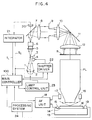
- Figure 4 shows the construction of a projection exposure apparatus according to an embodiment of the present invention.
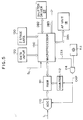
- Figure 5 is a block diagram showing the construction of the main control system in Figure 4.
- Figures 6A - 6C are graphs showing an example of the illumination variation characteristic resulting from the opening-closing of a shutter and the driving characteristic of the Z stage.
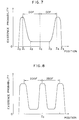
- Figure 7 is a graph showing the distribution of existence probability in Z direction (the direction of the optic axis) obtained under the movement conditions of Figure 6.
- Figure 8 is a graph showing the distribution when the exposure amount is concentrated in three locations in Z direction.
- Figure 9 is a graph showing the simulated distribution of existence probability.
- Figure 10 is a diagram showing the condition to simulate the distribution of light amount of a contact hole image.
- Figure 4 shows the construction of a projection exposure apparatus according to an embodiment of the present invention.
- illuminating light from a mercury discharge lamp 1 is condensed on a second focus by an elliptical mirror 2.
- a rotary shutter 3 having a plurality of blades is disposed near the second focus for rotation by a motor 4.
- the illuminating light condensed on the second focus and transmitted through the shutter 3 enters an optical integrator 6 including an input lens 5, a fly-eye lens, etc.
- a plurality of secondary light source images are formed on the exit surface side of the optical integrator 6, whereby a surface light source is made.
- the illuminating lights from the respective secondary light source images are reflected by a mirror 7 having a slight transmittance (e.g.
- the blind 9 is for limiting the illuminated range on a reticle R, and the opening image of the blind 9 is formed on the pattern surface of the reticle R through a second relay lens system 10, a mirror 11 and a condenser lens 12.
- the illuminating light transmitted through the transparent portion of the pattern of the reticle R passes through a projection lens PL to a wafer W, and the projected image of the reticle pattern is formed near the surface of the wafer W.
- the wafer W is vacuum-attracted onto the holder of a Z stage 14 disposed on an XY stage 13.
- the Z stage 14 is moved on the XY stage 13 in the direction of the optic axis of the projection lens PL by a driving portion (a motor and a tachogenerator) 15.
- the Z stage 14 is moved in the direction of the optic axis by the driving portion 15 being servo-operated under the control of an AF unit 18 which inputs a focus signal from an oblique incident light type AF sensor comprised of a light projector 16 and a light receiving device 17.
- an AF unit 18 which inputs a focus signal from an oblique incident light type AF sensor comprised of a light projector 16 and a light receiving device 17. This is an auto-focus operation effected during normal one-time exposure.
- a photoelectric sensor 19 for detecting the intensity of the illuminating light (the pattern image of the reticle R or the opening image of the blind 9) passed through the projection lens PL is provided on the XY stage 13.
- a photoelectric sensor 20 for detecting the intensity of part of the illuminating light passed through the shutter 3 is disposed rearwardly of the mirror 7, and the photoelectric signal of the photoelectric sensor 20 is input to an integrator circuit 21 which digitally effects the integration of the quantity of light.
- the integrator circuit 21 outputs to a main control system 100 a signal IL obtained by the photoelectric signal being amplified by a predetermined amount.
- the signal IL is proportional to the illumination on the reticle R or the illumination on the wafer W.
- the integrator circuit 21 includes a comparison circuit which outputs the closing signal Sc of the shutter 3 from the main control system 100 when the value of a preset proper exposure amount and the integrated value of the quantity of light coincide with each other.
- This closing signal Sc is sent to a shutter driver 22, whereby the motor 4 is rotated by a predetermined amount to thereby close the shutter 3. Also, the driver 22 exchanges an opening command for the shutter 3, a shutter status signal, etc. between it and the main control system 100.
- the mercury discharge lamp (hereinafter simply referred to as the lamp) 1 has its supplied electric power controlled by a lamp control unit 23.
- a flash exposure system whereby the supplied electric power to the lamp 1 is increased to about twice the rated electric power only when the shutter 3 is open.
- the lamp control unit 23 is given a changeover command for the normal exposure system or the flash exposure system from the main control system 100, and in the case of flash exposure, it increases the supplied electric power to the lamp 1 in response to the start of the opening of the shutter 3.
- the XY stage 13 in Figure 4 steps so as to move respective ones of the plurality of shot areas on the wafer W to just beneath the projection lens PL, but this is not directly related to the present invention and therefore, the driving portion and the control system for the XY stage 13 are not shown.
- an analog-digital converter ADC 110 receives as an input the amplified photoelectric signal IL from the photoelectric sensor 20, and converts the level of the signal IL into a digital value during each predetermined sampling time.
- the converted digital value is stored in a memory (RAM) 111 in order of address.
- the address value of the RAM 111 is generated by a counter 112, and this counter 112 counts the pulse number of a clock pulse CKP made by a clock generator 113 only while the clock pulse CKP passes through a gate 114.
- the opening and closing of the gate 114 are changed over by a signal CS, from a microprocessor ( ⁇ P) 150.
- This microprocessor ⁇ p 150 is connected to both of the AF unit 18 and the shutter driver 22 in Figure 4 through bus lines DB 1 and DB 2 , and effects the exchange of data necessary for control.
- a data input portion (or a man machine interface) 120 receives as inputs commands and data from the operator, and main commands are a changeover command for multiplex exposure or normal exposure and an exposure starting command, and main data are the proper (target) exposure amount per shot and the movement width (2Z 1 ) of the Z stage 14 during multiplex exposure.
- a Z stage characteristic data portion 130 stores therein chiefly the data of the movement speed characteristic of the Z stage 14 (the maximum speed value, the acceleration value, etc.).
- the data of this speed characteristic can be easily found by converting the output value from the tachogenerator provided in the driving portion 15 for the Z stage 14 into a digital value by an A/D converter during each predetermined sampling time, and reading the digital value into the memory in the microprocessor ⁇ p 150 through the bus line DB 1 , and thereafter analyzing it by the microprocessor ⁇ P 150.
- the data thus found by the microprocessor ⁇ p are stored in the Z stage characteristic data portion 130, but the Z stage may sometimes differ in its speed characteristic between a case where it is moved from below to above and a case where it is moved from above to below and therefore, it is preferable to find and store speed characteristics with respect to the both cases.
- the microprocessor ⁇ p 150 controls the stoppage of the outputting of the signal CS 1 to the gate 114 on the basis of the inputting of the closing signal Sc of the shutter 3. Further, the microprocessor ⁇ P 150 outputs various warnings to the operator through a bus line DB 3 . As one of the warnings, it is reported that it is difficult to effect multiplex exposure under exposure conditions input to the data input portion 120 and accordingly, it is necessary to revise some of the conditions.
- the microprocessor ⁇ P 150 Prior to exposure, the microprocessor ⁇ P 150 sets the value of the proper exposure amount input to the data input portion 120 in one input of the comparison circuit of the integrator circuit 21 and also outputs an opening command for the shutter 3 to the shutter driver 22 through the bus line DB 2 in the one-time exposure mode with the wafer W being absent under the projection lens PL. Thereby, the shutter driver 22 controls the closing of the shutter 3 so that the exposure amount on the reticle R or the wafer W may be a proper value.
- the microprocessor ⁇ P 150 delivers the signal CS 1 to the gate 114 simultaneously with the generation of the opening command for the shutter, and starts the counting up by the counter 112. The counting up by the counter 112 is stopped by the outputting of the signal CS 1 being discontinued in a predetermined time after the shutter closing signal Sc is produced. That predetermined time is made somewhat longer than the operational delay (electrical and mechanical delay) during the closing of the shutter.
- an illumination variation characteristic P(t) on the reticle is obtained in the RAM 111 in Figure 5 as shown, for example, in Figure 6A.
- the ordinate of this characteristic P(t) represents the illumination value
- the abscissa represents time and it is to be understood that, at.a. time t SO , the signal CS 1 in Figure 5 is produced and the counting up by the counter 112 is started.
- a time t SC in Figure 6A represents a point of time at which the shutter closing signal Sc is produced from the integrator circuit 21.
- a time t 0 on the characteristic P(t) represents a point of time at which the illuminating light passed through the shutter 3 actually begins to be applied to the reticle R, and has a substantially constant delay with respect to the time t SO when the signal CS 1 which is an exposure starting command is produced.
- the time t 5 when the applications of the exposure light to the reticle R is completely discontinued has a substantially constant delay with respect to the time t SC when the signal Sc is produced.
- the total exposure amount (proper exposure amount) Eu provided to the wafer W is expressed as follows with k as a constant:
- the microprocessor ⁇ P 150 shown in Figure 5 calculates delay times (t 0 - t SO ) and (t 5 - t SC ) in the characteristic P(t) and the acceleration of the variation in illumination from the shutter opening operation starting time t 0 till the shutter closing completion time t 5 , on the basis of the data stored in the RAM 111, and stores them in the memory in the microprocessor ⁇ P 150.
- Figure 6B shows an example of the characteristic V(t) when during the exposure operation, the Z stage 14 is moved at a special speed pattern in the direction of the optic axis on the basis of the speed data stored in the Z stage characteristic data portion 130.
- the Z stage 14 begins to be moved at a low speed v 1 at a time t S before the time t 0 when the shutter opening command is generated, and keeps the speed v 1 from the time t 0 till a time t 1 which is a predetermined time after the time t 0 , and accelerates to a speed v 2 approximate to the highest speed from after the time t 1 .
- the Z stage decelerates again to a low speed v 3 (substantially equal to v 1 ) from after a time t 3 after the Z stage is stabilized at the speed v 2 , and is maintained at the speed v 3 until the closing of the shutter is completed.
- Figure 6C shows the position characteristic Z(t) of the Z stage 14 in the direction of the optic axis when the Z stage 14 is moved at the characteristic V(t) of Figure 6B.
- a position ZC is a position at which the pattern projection image of the reticle R coincides with the surface of the wafer as the best image.
- the speed of the Z stage 14 is brought into the highest state near the position at which the best image plane coincides with the surface of the wafer, and is kept at the lowest possible speed during the opening and closing operations of the shutter 3. That is, during one shutter opening operation, the Z stage 14 is moved while being accelerated and decelerated at a predetermined characteristic.
- the step of introducing the illumination characteristic P(t) into the RAM 111 and calculating various data may be suitably executed plural times and the result may be averaged.
- the opening-closing of the shutter 3 is controlled so that a proper exposure amount may be obtained from first by the integrator circuit 21, but in the case of a mode in which the opening-closing of the shutter 3 is controlled by time, the set shutter time can be adjusted until a proper exposure amount is obtained, and after the proper exposure amount is obtained, the characteristic P(t) of Figure 6A can be stored in the RAM 111.
- the characteristic P(t) to be stored in the RAM 111 may be made from the photoelectric signal of the photoelectric sensor 19 obtained through a processing system 24.
- the wafer W is at a position Zs before the exposure is started, and the wafer W starts movement in the Z direction (the direction of the optic axis) from here.
- the Z stage 14 at the position Zs starts to be driven at a time t S , and is uniformly moved at a low speed v 1 .
- the shutter opening command (signal CS 1 ) is output at a time t SO so that the shutter 3 may begin to be opened after the speed of the Z stage 14 is stabilized at v 1 .
- the wafer W is uniformly moved at the speed v 3 , and at a time t SC , the shutter closing command (signal Sc) is output.
- exposure amounts E 1 and E 4 provided to the wafer W at the positions Z 0 , Z 1 , Z 4 and Z 5 and between the positions Z 0 - Z 1 and between the positions Z 4 - Z 5 greatly contribute to the enlargement of the depth of focus.
- the exposure amount provided to the wafer W while the Z stage 14 is moved from the position Z 1 to the position Z 4 is about 30% of the total exposure amount Eu.
- the numerical values (parameters) shown above by way of example are standard values to the last, and can be suitably changed by the operator. However, if the parameters are changed at random, it does not always follow from various limitations (such as the speed and movement stroke of the Z stage and the illumination) that the conditions are properly set. In that case, as will be described later in detail, a warning is generated through the bus line DB 3 to inform the operation that the proper setting of the conditions is impossible by the parameters changed by the operator.
- the time t 1 when the exposure amount integrated from the exposure starting time t 0 (the integrated value) becomes E 1 can be found from the relation of the following equation (in which k 1 is a constant), on the basis of the illumination variation characteristic P(t) stored in the RAM 111:
- the spacing between the positions Z 0 and Z 1 may preferably be as small as possible relative to the depth of focus DOF (ZC - Z 0 , Z 5 - ZC) of the projection lens PL, and as an example, may desirably be 1/3 or less of the value DOF.
- the time t 4 when the exposure amount (integrated value) provided to the wafer W from the time t 4 till the time t 5 becomes E 4 is inversely calculated from the relation of the following equation (in which k 2 is a constant) on the basis of the illumination variation characteristic P(t):
- the time t 5 is known, and is already prescribed on the characteristic P(t) stored in the RAM 111.
- the spacing between the positions Z 4 and Z 5 may also desirably be 1/3 or less of the depth of focus DOF of the projection lens PL.
- the time (t 2 - t 1 ) and the time (t 4 - t 3 ) are substantially constant values and thus, when the total of the time (t 2 - t 1 ) and the time (t 4 - t 3 ) becomes greater than the time T ⁇ , the control of the Z stage becomes unstable and the expected depth enlarging effect cannot be attained.
- the microprocessor ⁇ P 150 finds the relation among the acceleration discontinuing time t 2 and the deceleration starting time t 3 of the Z stage 14 and the speed v 2 .
- equation (10) becomes a relational expression having v 2 , t 2 and t 3 as parameters.
- the time t 3 will be correspondingly determined and the positions and the driving conditions of the Z stage at the respective times during exposure (t 0 - t 5 ) will be accurately determined.
- the best focus position ZC lies substantially at the midpoint between the positions Z 1 and Z 4 and therefore, as shown in Figure 6C, the position characteristic Z(t) becomes a curve substantially point-symmetrical about the position ZC.
- the accelerations a and ⁇ of the Z stage may be fixed at predetermined values in advance on the basis of equations (9), (2) and (3) and the times t 2 and t 4 may be determined in conformity with the value of the speed v 2 from equations (2) and (3), whereby the driving conditions can likewise be found accurately.
- the movement conditions including the movement speed of the wafer W in the Z direction during exposure and the Z position are determined, exposure may thereafter be effected in accordance with the determined conditions, whereby between the positions Z 0 to Z 1 , the exposure amount E 1 is accurately provided to the wafer W, and between the positions Z 4 to Z 5 , the exposure amount E 4 is accurately provided to the wafer W.
- the total exposure amount Eu is also controlled accurately.
- the initial position of the Z stage 14 has been shown as Z S but alternatively, the initial position may be a position above Z 5 and with the progress of exposure, the Z stage may be moved reversely to Z 4 , Z 3 , ..., Z 0 .
- the Z position of the Z stage during exposure can be detected by the AF unit 18 shown in Figure 4, but if the movement width (2 ⁇ DOF) of the Z stage during exposure is great, the Z position may exceed the detection range of the AF sensor. In such case, the focus signal cannot be obtained near the positions Z 1 and Z 4 and therefore, design can be made such that the positional information is obtained from a potentiometer or a position sensor which monitors the amount of driving of the Z stage.
- the focus signal assumes a state representative of in-focus (for example, the zero point) is checked up while the level of the surface of the wafer W is being monitored by an AF sensor, and whether this time is substantially at the midpoint between the times t 2 and t 3 is judged, whereby whether the exposure operation for one shot has been effected well can be roughly known.
- a state representative of in-focus for example, the zero point
- Figure 7 graphically shows the existence probability of the wafer (or concentration of the exposure amount) with respect to the Z direction when exposure is effected at the characteristics shown in Figures 6A, 6B and 6C. From the fact that the peaks of the existence probability exist near the positions Z 0 - Z 1 and near the positions Z 4 - Z 5 , the enlargement of the depth of focus can be achieved. In the present embodiment, the exposure amount cannot be made zero at the positions between the peaks, e.g. Z 2 - Z 3 . This is because the Z stage is continuously moved.
- Figure 8 shows the existence probability of the wafer when the number of times of multiplex exposure is three, and represents a case where as the driving pattern of the Z stage 14 when the shutter is open, the low speed uniform movement ⁇ acceleration and deceleration ⁇ the low speed uniform movement are repeated twice. Peaks exist at three locations with respect to the position in the Z direction, and the central peak is adjusted to the best focus position ZC, and the peaks on the opposite sides of the central peak are spaced apart from each other by an amount corresponding to the depth-of-focus width 2 ⁇ DOF of the projection lens PL. Again in this case, it is more desirable that the exposure amounts corresponding to the three peaks be uniform.
- the characteristic P(t) of Figure 6A is proportionally enlarged in the direction of the time axis with the deterioration of the lamp intensity and therefore, after one lot of wafers (25 wafers) have been treated, the characteristic P(t) should preferably be re-measured. Also, after the characteristic P(t) has been stored in the RAM 111, it is better to adopt a timer mode in which the operation of the shutter 3 is controlled by time, and control the time t so - t sc so as to be set as the shutter time.
- the warning is produced when the time from the opening start time t 0 of the shutter 3 till the closing completion time t 5 of the shutter 3 becomes considerably short as compared with the movement speed variation pattern of the Z stage 14.
- the time t 1 - t 4 becomes so short that the constant high speed range (speed v 2 ) as shown in 6B does not exist, the range in which a minimum existence probability is provided between the positions Z 2 - Z 3 as shown in Figure 7 becomes null and the effect of enlarging the depth of focus cannot sufficiently obtained.
- the actual exposure time (t 0 - t 5 ) for the wafer W can be lengthened until good control becomes possible.
- the exposure time per one shot becomes slightly longer and some reduction in throughput is caused, but the reduction in throughput heretofore experienced can be avoided.
- an ND filter for stepwisely changing the intensity of the illuminating light is removably provided in the illuminating optical system of the projection exposure apparatus.
- the transmittance of the ND filter light may be decreased, for example, at every 10% and finally to the order of 50%.
- the illumination characteristic P(t) can be again stored in the RAM 111 and similar calculation can be executed.
- Figure 9 shows the characteristic of the existence probability simulated on the basis of the position characteristic Z(t) of the Z stage and is the same one as shown in Figure 7.
- the existence probability from times t 0 to t 5 is shown, and the existence probability is constant in the low speed uniform movement ranges from times t 0 to t 1 and from times t 4 to t 5 .
- changes in illumination at the rise and the fall of the illumination characteristic P(t) are neglected, and it is assumed that the illumination is constant over time interval from t 0 to t 5 (where the shutter is fully opened).
- the existence probability is defined as time ⁇ t required for unit displacement ⁇ Z in the Z direction, and is treated as ⁇ t/ ⁇ Z.
- the intensity distribution in the optic axis in the center of the projection image or in the neighborhood thereof of one contact hole pattern may be considered to take approximately a Gaussian distribution because the size of the pattern is close to the resolution limit of the projection lens.
- Figure 10 is the result of simulation on the distribution of the quantity of light by the contact hole image in the direction of the optic axis.
- the distribution of the quantity of light in the direction of the optic axis may be obtained by convolution of the product of the existence probability characteristic (function) shown Figure 9 and the function of the Gaussian distribution.
- Gaussian distribution curve GP(Z) is so shifted in the Z direction along the curve of'the existence probability that the peak of the curve GP(Z) at each point in the Z direction may be located on the curve of the existence probability, and the Gaussian distribution curves thus obtained are summed to obtain the light quantity distribution IM(Z).
- the light guantity distribution IM(Z) is substantially flat in the movement range on width from Z 0 to Z 5 of the Z stage. This means that, when the projection image plane is set to a position ZC and the surface of the wafer is shifted between the positions Z 0 and Z 5 , the quantity of light of the contact hole image applied to the resist layer is substantially constant. In other words, the fact that the quantity of light (the contact hole image) is substantially constant over the long range in the direction of the optic axis, means that the apparent depth of focus is made larger to that extent.
- the ratio (Z-Span/2 ⁇ DOF) of the movement range Z-span of the Z stage from the position Z 0 to the position Z 5 to the "depth of focus" width 2 ⁇ DOF of the single unit of the projection lens is about 2.24. This is because, during exposure operation from the position Z 0 to the position Z 5 , the shutter is fully opened and the illumination is constant, and actually the ratio is slightly smaller.
- the optimum value of the movement range of the Z stage can be obtained. If the ratio Z-Span/2 ⁇ DOF is made smaller from the stage shown in Figure 10, the light quantity distribution IM(Z) rapidly changes to form a Gaussian distribution peaked at the position ZC. If the ratio Z-Span/2 ⁇ DOF is made larger, the light quantity distribution IM(Z) falls at the position ZC and has the peaks between the position Z 0 and ZC and between the positions ZC and Z 5 . According to the experiments, it has been formed that, in the case of the contact hole pattern, if the movement range of the Z stage is so determined that the light quantity distribution is substantially flat, the apparent depth of focus is sufficiently extended and further the deterioration of contrast is made minimum.
- a software for carrying out the simulation as shown in Figure 10 is provided in the stepper, by which the existence probability chacteristic curve is produced based on various parameters under the exposure condition designated by user and the Gaussian distribution GP(Z) is shifted in the Z direction along the existence probability curve, thereby calculating the quantity distribution IM(Z) of the contact hole pattern, where the peak of each Gaussian distribution is made coincident with the curve of the existence probability when the shutter is in the fully opened state, while during the opening operation or closing operation of the shutter the peak of each Gaussian distribution is adjusted to be on a point lowered from the value of the existence probability to the extent of the lowered amount from the illumination obtained at the time when the shutter is fully opened.
- the thus obtained light quantity distribution IM(Z) is displayed by a cathode-ray tube or the like on the control panel of the stepper, and the width in the Z direction of the flat portion which is within the tolerance range is calculated and displayed. This is advantageous because the operator can confirm previously whether the optimum result is expected under the set exposure condition, and that resetting of another exposure condition can be easily made.
- anouncing to the operator may be made to notice that there is any problem on exposure condition in view of the characteristic of the light quantity distribution IM(Z) obtained by the simulation.
- the substantially constant light quantity distribution in the Z direction as shown in Figure 10 is particularly advantageous in the case where the wafer surface has continuous uneveness since the pattern is formed accurately with respect to each of uneven or stepped portions on the wafer surface.
- steps or uneven portions are located mainly at the memory cell portion and the peripheral circuit portions as in the case of DRAM pattern, it is not necessary to make the light quantity distribution of the contact hole image constant in the Z direction, but rather it may be so set that the light quantity distribution is larger at two portions, the higher portion (memory call portion) and the lower portion (peripheral circuit) of the stepped portions.
- the movement range Z-Span of the Z stage may be extendned.
- the projection image plane and the photosensitive substrate are moved relative to each other in the direction of the optic axis at a pre-controlled speed characteristic and therefore, the effect of enlarging the depth of focus can be attained without extremely reducing the photosensitive substrate treating ability (throughput) per unit time.
- the illumination variation characteristic of the illuminating light on the mask is found in advance before the main exposure to the photosensitive substrate and therefore, the desired exposure amounts (E 1 , E 4 , etc.) input by the operator can be exactly concentrated on particular points (two or three points) within the focus range set by the operator and at the same time, the total exposure amount for one shot area can also be accurately controlled.
Landscapes
- Physics & Mathematics (AREA)
- General Physics & Mathematics (AREA)
- Health & Medical Sciences (AREA)
- Life Sciences & Earth Sciences (AREA)
- Atmospheric Sciences (AREA)
- Toxicology (AREA)
- Engineering & Computer Science (AREA)
- Environmental & Geological Engineering (AREA)
- Epidemiology (AREA)
- Public Health (AREA)
- Exposure And Positioning Against Photoresist Photosensitive Materials (AREA)
- Exposure Of Semiconductors, Excluding Electron Or Ion Beam Exposure (AREA)
Claims (6)
- Appareil d'exposition par projection doté d'un système d'éclairage pour éclairer un masque (R) formé d'un motif prédéterminé, d'un obturateur (3) pour inverser l'application de la lumière d'éclairage audit masque (R) et l'interception de la lumière d'éclairage, d'un système optique de projection (PL) pour projeter l'image du motif dudit masque, d'une platine mobile (14) maintenant un substrat photosensible (W) près du plan image de projection dudit système optique de projection (PL) et capable de déplacer ledit substrat photosensible (W) dans la direction de l'axe optique tandis que ledit obturateur (3) est ouvert, d'un moyen de commande de la platine (18) pour commander ladite platine mobile au moyen d'une caractéristique de fonctionnement, et d'un moyen de commande de l'obturateur (22) pour commander l'ouverture-fermeture dudit obturateur à partir de la quantité d'un degré d'exposition dudit substrat, caractérisé par le fait de prévoir un moyen d'enclenchement (100) pour enclencher les opérations dudit moyen de commande de l'obturateur (22) et dudit moyen de commande de la platine (18) afin que d'après la caractéristique de fonctionnement dudit obturateur (3) et la caractéristique de fonctionnement de ladite platine mobile (14), la répartition d'une probabilité d'existence dudit substrat (W) obtenue lors du déplacement dudit substrat (W) avec ladite platine entre l'instant de démarrage de l'opération d'ouverture et l'instant d'achèvement de l'opération de fermeture dudit obturateur (3), par rapport à la direction de l'axe optique, puisse admettre des valeurs maximales à peu près égales à au moins deux emplacements dans la direction de l'axe optique.
- Appareil d'exposition par projection selon la revendication 1, caractérisé en ce que ledit obturateur (3) est doté d'une caractéristique de fonctionnement telle que le temps de l'opération d'ouverture entre l'instant de démarrage de l'opération d'ouverture et l'instant d'achèvement de l'opération d'ouverture et le temps de l'opération de fermeture entre l'instant de démarrage de l'opération de fermeture et l'instant d'achèvement de l'opération de fermeture deviennent pratiquement égaux l'un à l'autre, et ledit moyen d'enclenchement (100) comprend une partie de commande d'enclenchement de vitesse (130) pour définir la vitesse de déplacement de ladite platine mobile (14) afin que les premières valeurs à l'instant du démarrage de l'opération de l'ouverture et à l'instant de l'achèvement de l'opération de fermeture dudit obturateur (3) soient sensiblement égales, et pour régler la vitesse de déplacement de ladite platine mobile (14) à une deuxième valeur supérieure auxdites premières valeurs dans la section existant dans l'intervalle entre l'instant d'achèvement de l'opération d'ouverture et l'instant de démarrage de l'opération de fermeture dudit obturateur (3).
- Appareil d'exposition par projection selon la revendication 2, caractérisé en ce que ladite partie de commande d'enclenchement de vitesse (130) définit la vitesse de déplacement de ladite platine mobile (14) afin que le temps entre l'instant de démarrage de l'opération d'ouverture et le début de ladite seconde valeur de déplacement et le temps entre la fin de ladite deuxième valeur de déplacement et l'instant d'achèvement de l'opération de fermeture soient à peu près égaux l'un à l'autre.
- Appareil d'exposition par projection selon la revendication 2, caractérisé en ce que ledit moyen d'enclenchement (100) comporte une partie de calcul (150) pour calculer le temps d'exposition entre ledit instant de démarrage de l'opération d'ouverture et ledit instant d'achèvement de l'opération de fermeture nécessaire pour fournir une exposition correcte audit substrat photosensible, et une partie d'évaluation (150) pour évaluer s'il y a une différence entre ledit temps d'exposition et le temps nécessaire à ladite platine mobile (14) pour exécuter la modification de vitesse déterminée par ladite partie de commande d'enclenchement de vitesse (130), et délivrer un signal d'avertissement (DB3) représentant la commande entraínant le non enclenchement quand ledit temps d'exposition est plus court que ledit temps nécessaire.
- Appareil d'exposition par projection selon la revendication 4, caractérisé en ce que ledit moyen d'enclenchement (100) inclut une partie de régulation de l'intensité d'éclairement pour réguler l'intensité de la lumière d'éclairage vers ledit masque conformément audit signal d'avertissement.
- Procédé de fabrication d'un composant de circuit sur un substrat (W) en utilisant un appareil d'exposition doté d'un système de projection pour projeter une image du motif du composant sur une surface sensible du substrat (W), le procédé comprenant les étapes consistant à:dans lequel ladite grande vitesse est maintenue entre les étapes (c) et (d) et la surface du substrat traverse ledit meilleur plan image (Zc) à ladite grande vitesse environ audit point milieu de la période de temps d'exposition.(a) placer le substrat (W) sous ledit système de projection afin que la surface du substrat soit positionnée à une première position relative à un côté d'un meilleur plan d'image (Zc) dudit système de projection;(b) démarrer une opération d'exposition pour projeter l'image du motif sur le substrat par l'intermédiaire d'un système de projection pendant une période de temps d'exposition prédéterminée;(c) démarrer une accélération de la surface du substrat relative au meilleur plan image (Zc) afin que la surface du substrat accélère en direction d'une deuxième position relative à l'autre côté dudit meilleur plan image (Zc), afin de parvenir à une grande vitesse à peu près constante de la surface du substrat par rapport au meilleur plan image (Zc) au niveau d'un temps avant d'atteindre le point milieu de ladite période de temps d'exposition; et(d) démarrer une décélération de la surface du substrat par rapport au meilleur plan image (Zc) depuis ladite grande vitesse au niveau d'un temps entre ledit point milieu et un point terminal de la période de temps d'exposition,
Priority Applications (1)
| Application Number | Priority Date | Filing Date | Title |
|---|---|---|---|
| EP97202676A EP0819988A1 (fr) | 1990-10-30 | 1991-10-30 | Appareil de projection pour exposition |
Applications Claiming Priority (4)
| Application Number | Priority Date | Filing Date | Title |
|---|---|---|---|
| JP29316290 | 1990-10-30 | ||
| JP293162/90 | 1990-10-30 | ||
| JP23153091A JP3234891B2 (ja) | 1990-10-30 | 1991-09-11 | 投影露光装置 |
| JP231530/91 | 1991-09-11 |
Related Child Applications (1)
| Application Number | Title | Priority Date | Filing Date |
|---|---|---|---|
| EP97202676A Division EP0819988A1 (fr) | 1990-10-30 | 1991-10-30 | Appareil de projection pour exposition |
Publications (3)
| Publication Number | Publication Date |
|---|---|
| EP0484131A2 EP0484131A2 (fr) | 1992-05-06 |
| EP0484131A3 EP0484131A3 (en) | 1992-09-09 |
| EP0484131B1 true EP0484131B1 (fr) | 1998-05-06 |
Family
ID=26529934
Family Applications (2)
| Application Number | Title | Priority Date | Filing Date |
|---|---|---|---|
| EP97202676A Withdrawn EP0819988A1 (fr) | 1990-10-30 | 1991-10-30 | Appareil de projection pour exposition |
| EP19910310024 Expired - Lifetime EP0484131B1 (fr) | 1990-10-30 | 1991-10-30 | Appareil de projection pour exposition |
Family Applications Before (1)
| Application Number | Title | Priority Date | Filing Date |
|---|---|---|---|
| EP97202676A Withdrawn EP0819988A1 (fr) | 1990-10-30 | 1991-10-30 | Appareil de projection pour exposition |
Country Status (3)
| Country | Link |
|---|---|
| EP (2) | EP0819988A1 (fr) |
| JP (1) | JP3234891B2 (fr) |
| DE (1) | DE69129355T2 (fr) |
Cited By (1)
| Publication number | Priority date | Publication date | Assignee | Title |
|---|---|---|---|---|
| CN1595300B (zh) * | 2003-09-10 | 2010-11-17 | Asml荷兰有限公司 | 衬底曝光方法和光刻投影设备 |
Families Citing this family (8)
| Publication number | Priority date | Publication date | Assignee | Title |
|---|---|---|---|---|
| JP2705312B2 (ja) * | 1990-12-06 | 1998-01-28 | ソニー株式会社 | 投影露光方法 |
| KR100538685B1 (ko) * | 1993-04-06 | 2006-09-14 | 가부시키가이샤 니콘 | 투영노광장치, 노광방법, 및 소자 제조 방법 |
| JPH09320921A (ja) * | 1996-05-24 | 1997-12-12 | Nikon Corp | ベースライン量の測定方法及び投影露光装置 |
| JP3796367B2 (ja) | 1999-03-09 | 2006-07-12 | キヤノン株式会社 | ステージ制御方法、露光方法、露光装置およびデバイス製造方法 |
| WO2019079010A1 (fr) | 2017-10-19 | 2019-04-25 | Cymer, Llc | Formation de multiples images aériennes en un seul passage d'exposition lithographique |
| JP7261089B2 (ja) | 2019-05-29 | 2023-04-19 | 旭化成株式会社 | フレキソ印刷原版、及びフレキソ印刷版の製造方法 |
| US20250319715A1 (en) | 2022-05-18 | 2025-10-16 | Asahi Kasei Kabushiki Kaisha | Original flexographic printing plate, method for producing flexographic printing plate, flexographic printing plate and flexographic printing method |
| CN121079639A (zh) | 2023-04-25 | 2025-12-05 | 旭化成株式会社 | 柔性印刷原版和柔性印刷版的制造方法 |
Family Cites Families (3)
| Publication number | Priority date | Publication date | Assignee | Title |
|---|---|---|---|---|
| JPS5817446A (ja) * | 1981-07-24 | 1983-02-01 | Hitachi Ltd | 投影露光方法および装置 |
| US4869999A (en) * | 1986-08-08 | 1989-09-26 | Hitachi, Ltd. | Method of forming pattern and projection aligner for carrying out the same |
| JP2705312B2 (ja) * | 1990-12-06 | 1998-01-28 | ソニー株式会社 | 投影露光方法 |
-
1991
- 1991-09-11 JP JP23153091A patent/JP3234891B2/ja not_active Expired - Lifetime
- 1991-10-30 EP EP97202676A patent/EP0819988A1/fr not_active Withdrawn
- 1991-10-30 DE DE69129355T patent/DE69129355T2/de not_active Expired - Fee Related
- 1991-10-30 EP EP19910310024 patent/EP0484131B1/fr not_active Expired - Lifetime
Cited By (1)
| Publication number | Priority date | Publication date | Assignee | Title |
|---|---|---|---|---|
| CN1595300B (zh) * | 2003-09-10 | 2010-11-17 | Asml荷兰有限公司 | 衬底曝光方法和光刻投影设备 |
Also Published As
| Publication number | Publication date |
|---|---|
| EP0484131A2 (fr) | 1992-05-06 |
| EP0819988A1 (fr) | 1998-01-21 |
| JP3234891B2 (ja) | 2001-12-04 |
| DE69129355D1 (de) | 1998-06-10 |
| DE69129355T2 (de) | 1998-10-22 |
| JPH0513305A (ja) | 1993-01-22 |
| EP0484131A3 (en) | 1992-09-09 |
Similar Documents
| Publication | Publication Date | Title |
|---|---|---|
| US5483311A (en) | Projection exposure apparatus | |
| EP0632331B1 (fr) | Appareil d'exposition et méthode de fabrication d'un microdispositif utilisant celui-ci | |
| US6335784B2 (en) | Scan type projection exposure apparatus and device manufacturing method using the same | |
| EP0484131B1 (fr) | Appareil de projection pour exposition | |
| US6127095A (en) | Illuminating optical device and semiconductor device manufacturing method | |
| US6151121A (en) | Position detecting system and device manufacturing method using the same | |
| US4652134A (en) | Mask alignment system | |
| US6501533B1 (en) | Scanning type exposure apparatus and method | |
| US6573977B1 (en) | Exposure control method, exposure apparatus and device manufacturing method | |
| US6172739B1 (en) | Exposure apparatus and method | |
| US6337734B1 (en) | Exposure control method, exposure apparatus and device manufacturing method | |
| US6195155B1 (en) | Scanning type exposure method | |
| JP3371406B2 (ja) | 走査露光方法 | |
| EP0720056B1 (fr) | Système d'illumination et appareil d'exposition par balayage | |
| US7046336B2 (en) | Scanning exposure apparatus | |
| JP2001326159A (ja) | レーザ装置、露光装置、および該露光装置を用いるデバイス製造方法 | |
| JP2000114164A (ja) | 走査型投影露光装置及びそれを用いたデバイスの製造方法 | |
| JP2001144009A (ja) | 露光方法及び露光装置、並びにデバイス製造方法 | |
| JPH0547625A (ja) | 投影露光装置 | |
| EP0748009B1 (fr) | Méthode de contrôle de sortie d'un laser à excimer | |
| JPH10106942A (ja) | 走査型露光装置及びそれを用いた半導体デバイスの製造方法 | |
| US5400109A (en) | Power-driven focusing apparatus | |
| JP2001257148A (ja) | 露光装置およびデバイス製造方法 | |
| JP2000260692A (ja) | 露光装置および露光方法 | |
| KR200272383Y1 (ko) | 반도체 소자 노광장치 |
Legal Events
| Date | Code | Title | Description |
|---|---|---|---|
| PUAI | Public reference made under article 153(3) epc to a published international application that has entered the european phase |
Free format text: ORIGINAL CODE: 0009012 |
|
| AK | Designated contracting states |
Kind code of ref document: A2 Designated state(s): DE FR GB IT NL |
|
| PUAL | Search report despatched |
Free format text: ORIGINAL CODE: 0009013 |
|
| AK | Designated contracting states |
Kind code of ref document: A3 Designated state(s): DE FR GB IT NL |
|
| 17P | Request for examination filed |
Effective date: 19930308 |
|
| 17Q | First examination report despatched |
Effective date: 19960625 |
|
| GRAG | Despatch of communication of intention to grant |
Free format text: ORIGINAL CODE: EPIDOS AGRA |
|
| GRAG | Despatch of communication of intention to grant |
Free format text: ORIGINAL CODE: EPIDOS AGRA |
|
| GRAH | Despatch of communication of intention to grant a patent |
Free format text: ORIGINAL CODE: EPIDOS IGRA |
|
| GRAH | Despatch of communication of intention to grant a patent |
Free format text: ORIGINAL CODE: EPIDOS IGRA |
|
| GRAH | Despatch of communication of intention to grant a patent |
Free format text: ORIGINAL CODE: EPIDOS IGRA |
|
| GRAA | (expected) grant |
Free format text: ORIGINAL CODE: 0009210 |
|
| AK | Designated contracting states |
Kind code of ref document: B1 Designated state(s): DE FR GB IT NL |
|
| DX | Miscellaneous (deleted) | ||
| REF | Corresponds to: |
Ref document number: 69129355 Country of ref document: DE Date of ref document: 19980610 |
|
| ITF | It: translation for a ep patent filed | ||
| ET | Fr: translation filed | ||
| PLBE | No opposition filed within time limit |
Free format text: ORIGINAL CODE: 0009261 |
|
| STAA | Information on the status of an ep patent application or granted ep patent |
Free format text: STATUS: NO OPPOSITION FILED WITHIN TIME LIMIT |
|
| 26N | No opposition filed | ||
| REG | Reference to a national code |
Ref country code: GB Ref legal event code: IF02 |
|
| PGFP | Annual fee paid to national office [announced via postgrant information from national office to epo] |
Ref country code: DE Payment date: 20051027 Year of fee payment: 15 |
|
| PG25 | Lapsed in a contracting state [announced via postgrant information from national office to epo] |
Ref country code: DE Free format text: LAPSE BECAUSE OF NON-PAYMENT OF DUE FEES Effective date: 20070501 |
|
| PGFP | Annual fee paid to national office [announced via postgrant information from national office to epo] |
Ref country code: FR Payment date: 20101020 Year of fee payment: 20 Ref country code: NL Payment date: 20101016 Year of fee payment: 20 |
|
| PGFP | Annual fee paid to national office [announced via postgrant information from national office to epo] |
Ref country code: GB Payment date: 20101027 Year of fee payment: 20 Ref country code: IT Payment date: 20101022 Year of fee payment: 20 |
|
| REG | Reference to a national code |
Ref country code: NL Ref legal event code: V4 Effective date: 20111030 |
|
| REG | Reference to a national code |
Ref country code: GB Ref legal event code: PE20 Expiry date: 20111029 |
|
| PG25 | Lapsed in a contracting state [announced via postgrant information from national office to epo] |
Ref country code: NL Free format text: LAPSE BECAUSE OF EXPIRATION OF PROTECTION Effective date: 20111030 |
|
| PG25 | Lapsed in a contracting state [announced via postgrant information from national office to epo] |
Ref country code: GB Free format text: LAPSE BECAUSE OF EXPIRATION OF PROTECTION Effective date: 20111029 |