EP0484129A2 - Abtast- und Halteschaltung - Google Patents
Abtast- und Halteschaltung Download PDFInfo
- Publication number
- EP0484129A2 EP0484129A2 EP91310021A EP91310021A EP0484129A2 EP 0484129 A2 EP0484129 A2 EP 0484129A2 EP 91310021 A EP91310021 A EP 91310021A EP 91310021 A EP91310021 A EP 91310021A EP 0484129 A2 EP0484129 A2 EP 0484129A2
- Authority
- EP
- European Patent Office
- Prior art keywords
- current
- circuit
- sample
- output
- input
- Prior art date
- Legal status (The legal status is an assumption and is not a legal conclusion. Google has not performed a legal analysis and makes no representation as to the accuracy of the status listed.)
- Granted
Links
- 239000003990 capacitor Substances 0.000 claims abstract description 57
- 239000000872 buffer Substances 0.000 claims description 47
- 238000007599 discharging Methods 0.000 claims description 7
- 238000005070 sampling Methods 0.000 claims description 6
- 230000004044 response Effects 0.000 claims description 4
- 230000007423 decrease Effects 0.000 description 21
- 238000010586 diagram Methods 0.000 description 12
- 230000003071 parasitic effect Effects 0.000 description 10
- 101150086309 MUB1 gene Proteins 0.000 description 7
- 101150033166 MUB2 gene Proteins 0.000 description 7
- 230000001965 increasing effect Effects 0.000 description 7
- 101100340318 Arabidopsis thaliana IDL2 gene Proteins 0.000 description 6
- 101150095437 MUB3 gene Proteins 0.000 description 6
- 230000003247 decreasing effect Effects 0.000 description 6
- NJPPVKZQTLUDBO-UHFFFAOYSA-N novaluron Chemical compound C1=C(Cl)C(OC(F)(F)C(OC(F)(F)F)F)=CC=C1NC(=O)NC(=O)C1=C(F)C=CC=C1F NJPPVKZQTLUDBO-UHFFFAOYSA-N 0.000 description 5
- 230000008859 change Effects 0.000 description 3
- 230000000694 effects Effects 0.000 description 3
- 239000000758 substrate Substances 0.000 description 3
- 238000002955 isolation Methods 0.000 description 2
- 230000000903 blocking effect Effects 0.000 description 1
- 230000000593 degrading effect Effects 0.000 description 1
- 230000002708 enhancing effect Effects 0.000 description 1
- 238000009413 insulation Methods 0.000 description 1
- 238000000034 method Methods 0.000 description 1
- 230000002093 peripheral effect Effects 0.000 description 1
- 230000009467 reduction Effects 0.000 description 1
- 230000000630 rising effect Effects 0.000 description 1
- 239000004065 semiconductor Substances 0.000 description 1
Images


Classifications
-
- G—PHYSICS
- G11—INFORMATION STORAGE
- G11C—STATIC STORES
- G11C27/00—Electric analogue stores, e.g. for storing instantaneous values
- G11C27/02—Sample-and-hold arrangements
-
- G—PHYSICS
- G11—INFORMATION STORAGE
- G11C—STATIC STORES
- G11C27/00—Electric analogue stores, e.g. for storing instantaneous values
- G11C27/02—Sample-and-hold arrangements
- G11C27/024—Sample-and-hold arrangements using a capacitive memory element
Definitions
- the present invention relates to a sample-and-hold circuit.
- sample-and-hold circuits Various types are known. Of these circuits, the "diode-bridge sample-and-hold circuit" can operate at high speed with high accuracy.
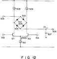
- the conventional diode-bridge sample-and-hold circuit has an input terminal 505, an output terminal 506, a capacitor 507 connected to the output terminal 506, three constant-current source circuits 508 to 510, two transistors 511 and 512 used as switching transistors, and a diode-bridge circuit as shown in Fig. 12.
- the diode-bridge circuit comprises four diodes 501 to 504.
- the common node of the first and second diodes 501 and 502 is connected to the input terminal 505, and the common node of the second and third diodes 503 and 504 is connected to the output terminal 506.
- the common node of the first and third diodes 501 and 503 is connected to the first constant-current source 508 and also to the collector of the first switching transistor 511.
- the common node of the second and fourth diodes 502 and 504 is connected to the second constant-current source circuit 509 and also to the collector of the second switching transistor 512.
- the emitters of both switching transistors 511 and 512 are connected to the constant current-supply circuit 510.
- Two clock signals 513 and 514 180° out of phase with respect to each other, are input to the bases of the transistors 511 and 512, respectively.
- the transistors 511 and 512 are thereby operated in opposite phases, whereby the sample-and-hold circuit can operate in two modes, i.e., sample mode and hold modes.
- the sample-and-hold circuit is set in the sample mode. More precisely, once the first and second transistors 511 and 512 are turned off and on, respectively, the current Ibias supplied from the third constant-current source circuit 510 flows through the second switching transistor 512, biasing all diodes 501 to 504. If the signal at the input terminal 505 is constant with respect to time, the current Ibias/2 from the first constant current-source circuit 508 flows divides equally between the first and second diodes 501 and 502, and the third and fourth diodes 503 and 504, such that Ibias/A flows through each of the diodes 501 to 504.
- This current combines with the current Ibias/2 supplied from the second constant-current source circuit 509 to equal the current drawn by current source 510 through transistor 512, Ibias.
- Ibias current drawn by current source 510 through transistor 512
- no output current "Is" flows to the output terminal 506, and the potential at the capacitor 507 connected to the output terminal 506 does not change.
- the voltage at the output terminal 506 equals the voltage at the input terminal 505 because the voltage drop across diodes 502 and 504, and diodes 501 and 503 are equal due to their equal bias currents.
- the current from the input signal source increases the current through the second diode 502 to greater than Ibias/2 and decrease the current through the first diode 501 to less than Ibias/2 equally, by half of the amount supplied by the input signal source. Since the current flowing through the second switching transistor 512 is Ibias and the current supplied by the current source 509 is Ibias/2, the sum of the currents flowing through the diodes 501 and 504 must equal Ibias/2. Likewise, since no current is drawn by the transistor 511 and the current supplied by the current source 508 is Ibias/2, again, the sum of the currents flowing through the diodes 502 and 503 must equal Ibias/2.
- the current through the diode 504 must decrease by the same amount that the current through the diode 502 increases.
- the current through the diode 503 must increase by the same amount that the current through the diode 501 decreases.
- the resulting difference in current between the diodes 503 and 504, "Is" charges the capacitor 507 until its voltage, the output terminal 506, is equal to that of the input terminal 505.
- the voltage drop across the diodes 501 to 504 become equal, and their difference in currents become zero, thus, "Is" becomes zero and the circuit achieves a stable condition.
- the current drawn by the input signal source decreases the current through the second diode 502 to less than Ibias/2 and increases the current through the first diode 501 to greater than Ibias/2 equally, by half of the amount drawn by the input signal source.
- the sum of the currents flowing through the diodes 501 and 504 must equal Ibias/2, and the sum of the currents flowing through the diodes 502 and 503 must equal Ibias/2.
- the current through the diode 504 must increase by the same amount that the current through the diode 502 decreases.
- the charging-discharging current "Is” is equal to the input signal source current flowing into and out of the input terminal node 505. Furthermore, the maximum “Is” flows when the diodes 501 and 504 are off for an increasing input signal, or when the diodes 502 and 503 are off for a decreasing input signal. In the case of an increasing input signal, since the diode 501 is off, all of the current supplied by current source 508 flows into the diode 503. Since the diode 504 is off, the current through the diode 503 becomes “Is” and thus, the maximum value "Is” can achieve is Ibias/2. Likewise, for a decreasing input signal, the maximum value "Is" can achieve for discharging is also Ibias/2.
- the sample-and-hold circuit is set into the sample mode.
- the first and second transistors 501 and 502 are turned on and off, respectively, the first to fourth diodes 501 to 504 are turned off, essentially discounting the input terminal 505 from the output terminal 506, maintaining the potential of the capacitor 507.
- the sample-and-hold circuit is set into the hold mode.
- the conventional diode-bridge sample-and-hold circuit has the following drawbacks.
- the input impedance of the sample-and-hold circuit varies drastically when the operating mode is switched from the sample mode to the hold mode, and vice versa. This is because, in the diode bridge circuit, the input diodes 501 and 502 which are on in the sample mode are switched off i.e., open circuit, in the hold mode.
- a input buffer circuit is often added in front of the diode bridge circuit. This buffer circuit, however, increase the power consumption and noise of the circuit.
- the conventional diode-briddge sample-and-hold circuit suffers from two drawbacks, namely, insulation slew rate and a drastically varying input impedance.
- the object of the present invention is to provide a sample-and-hold circuit which achieves a high slew rate constant input impedance, without increasing the bias current of the switching diodes and, hence, the power consumption nor the DC and sample pedestal offset.
- a sample-and-hold circuit comprising: a diode circuit including first to fourth diodes connected in series; an input circuit connected, at one end, to the common node of the first and third diodes and, at the other end, to the common node of the second and fourth diodes; an output circuit connected to at least one of two nodes, the first of which is the common node of the first and second diodes, and the second of which is the common node of the third and fourth diodes; a current mirror circuit with one current mirror output terminal connected, to the common node of the first and third diodes and, the other current mirror output terminal connected to the common node of the second and fourth diodes; and a capacitor connected to the output terminal, wherein the current mirror circuit supplies the current mirror output terminal with an output current proportional to an input current signal.
- a sample-and-hold circuit comprising: a diode circuit including first to fourth diodes connected in series; an input circuit connected, at one end, to the common node of the first and third diodes and, at the other end, to the common node of the second and fourth diodes; first and second output terminals connected to the common node of the first and second diode and the node of the third and fourth diodes, respectively; a current mirror circuit with one current mirror output terminal connected, to the common node of the first and third diodes and, the other terminal of the current mirror output terminal, to the common node of the second and fourth diodes; and first and second capacitors connected to the first and second output terminals, respectively, wherein the first and second output terminal alternately deliver an output signal.
- an output voltage signal which is equal to the input voltage with respect to time, is supplied to the output terminal during the sample mode.
- the use of a current mirror to bias the first to fourth diodes also provides an effective way to detect quickly changing input signals and automatically increases the current bias level of the diodes to greatly reduce the charge and discharge time of the capacitor and thus, greatly increase the speed of the sample-and-hold circuit in the sample mode. Reduction of the charge and discharge time of the capacitor is important for output signal accuracy during high speed sample mode operation.
- an input circuit is incorporated to drive the first to fourth diodes to maintain a constant input impedance seen at the input terminal.
- the sample-and-hold circuit according to the second aspect of the invention retains all the advantages of the sample-and-hold circuit according to the first aspect of the invention, and also provides a second output terminal with a second capacitor in addition to the first output terminal and first capacitor, whereby the two output terminals and two capacitors operate in alternate modes. While the first output terminal and first capacitor are in the hold mode, the second output terminal and second capacitor are in the hold mode. In this way, at least one of the output terminals is providing an output signal at all times and therefore data can be read continuously from the sampe-and-hold circuit.
- Fig. 1 shows a sample-and-hold circuit according to the present invention.
- Fig. 1 shows, four diodes 101 to 104 are connected in series, forming a loop, or a switching circuit.
- the diodes 101 and 102 make a pair
- the diodes 103 and 104 make another pair. These diode pairs serve to achieve sampling operation and holding operation.
- the node 105 of the diodes 101 and 103 is connected to the emitter of an npn transistor 109, which in turn is connected to a sampling input terminal 111.
- the node 106 of the diodes 102 and 104 is connected to the emitter of an npn transistor 110, which in turn is connected to the sampling input terminal 111.
- the transistors 109 and 110 constitute an input stage of the sample-and-hold circuit.
- the node 107 of the diode 101 and 102 is connected to a first hold output terminal 112.
- a capacitor 113 is connected to the terminal 112 and functions as a hold capacitor.
- the node 108 of the diodes 103 and 104 is connected to a second hold output terminal 114.
- a capacitor 115 is coupled to the second hold output terminal 114 and functions as a hold capacitor.
- the sample-and-hold circuit has a current mirror circuit 116.
- the circuit 116 comprises a reference-current input terminal 117 and two output terminals 118 and 119.
- the input terminal 117 is connected to the collectors of the transistors 109 and 110.
- the first output terminal 118 is connected to the node 105 of the diodes 101 and 103.
- the second output terminal 119 is connected to the node 106 of the diodes 102 and 104.
- the sample-and-hold circuit further comprises npn transistors 120 and 121, two clock input terminals 122 and 123, and a constant-current source circuit 124.
- the transistors 120 and 121 operates differentially with respect to each other.
- the transistors 120 and 121 are connected, at base, to the clock input terminals 122 and 123, respectively.
- Two clock signals, which are out of phase, are supplied to the clock input terminals 122 and 123.
- the transistors 120 and 121 are connected, at collector, to the diode nodes 105 and 106, respectively, and connected, at emitter, to the constant-current source circuit 124.
- the circuit 124 biases both transistors 120 and 121.
- the sample-and-hold circuit constitutes the equivalent circuit shown in Fig. 2.
- the capacitor 113 connected to the output terminal 112 must be charged or discharged by current Is1.
- the speed of the sample-and-hold circuit is determined by how quickly the capacitor 113 can be charged or discharged, and therefore, is determined by the maximum absolute value of current Is1.
- the current flowing through the transistor 109 will increase to beyond Ibias/3, and thus, Ire > Ibias/3.
- the maximum charging current Is1 is Ibias/2 which occurs when the diode 101 cuts off and Ibias from the transistor 120 equals the sum of the current flowing though the transistor 109 Iref and the output current Iout1 of the first output 118 of the current mirror circuit 116.
- This maximum charging current Is1 can be increased to Ibias if the current mirror circuit 116 has a DC gain of one and an AC gain greater than 1 which increases with frequency.
- the current flowing through the transistor 109 will decrease to below ibias/3, and thus, Iref ⁇ Ibias/3.
- the discharging current Is1 will be Ibias - (Iref + Iout1 + Ibias/2).
- the diode pair 103 and 104 are reverse biased thus, the node 108 is essentially open circuited and the charge stored on the capacitor 115 is preserved, holding a constant voltage on the output terminal 114. Therefore, the sample-and-hold circuit operates in the hold more with respect to the output terminal 114.
- the transistors 120 and 121 are turned off and on, respectively. Then, the bias current Ibias supplied from the constant-current source circuit 124 flows through the collector-emitter path of the transistor 121. As a result, the transistor 110 and the diode pair 103 and 104 are forward biased. The transistor 109 is reverse biased and off, since the transistor 120 is off at this time. The diodes 101 and 102 are also cruse biased and off. In this condition, the sample-and-hold circuit constitutes the equivalent circuit shown in Fig. 3.
- the capacitor 115 connected to the output terminal 114 must be charged or discharged by current Is2.
- the speed of the sample-and-hold circuit is determined by how quickly the capacitor 115 can be charged or discharged, and therefore, is determined by the maximum absolute value of current Is2.
- the current flowing through the transistor 110 will increase to beyond Ibias/3, and thus, Iref > Ibias/3.
- the maximum charging current Is2 is Ibias/2 which occurs when the diode 104 cuts off and Ibias from the transistor 121 equals the sum of the current flowing through the transistor 110 Iref and the output current Iout1 of the second output 119 of the current mirror circuit 116.
- This maximum charging current Is2 can be increased to Ibias if the current mirror circuit 116 has a DC gain of one and an AC gain greater than one which increases with frequency.
- the current flowing through the transistor 110 will decrease to below Ibias/3, and thus, Iref ⁇ Ibias/3.
- the discharging current Is1 will be Ibias - (Iref + Iout1 + Iout2).
- the diode pair 102 and 101 are reverse biased thus, the node 107 is essentially open circuited and the charge stored on the capacitor 113 is preserved, holding a constant voltage on the output terminal 112. Therefore, the sample-and-hold circuit operates in the hold mode with respect to the output terminal 112.
- the sample-and-hold circuit of the invention is designed to operate in the sample mode with respect to one of the output terminals 112 and 114, while operating in the hold mode with respect to the other output terminal. Hence, it can sample the input signal, while outputting the data it holds.
- the sample-and-hold circuit can sample signals and output held data at high speed.
- the sample-and-hold circuit since the output currents of the current mirror circuit incorporated in the sample-and-hold circuit increases according to the input signal requirements, the sample-and-hold circuit has a greatly enhanced slew rate.
- the output terminals 118 and 119 of the current mirror 116 may be replaced by two constant-current source circuits, and the collectors of the input transistors 109 and 110 may be connected to an appropriate power supply.
- the maximum available current that charges or discharges the capacitor 113 will be Ibias/3, i.e., the standing current flowing through the diodes 101 and 102.
- currents Iref, Iout1 and Iout2 increase according to the requirements dictated by the input signal applied to the input terminal 111.
- current Is1 which changes the potential of the capacitor 113 and the output terminal 112 increases in accordance with the slew rate of the signal input to the input terminal 111.
- the slew rate of the sample-and-hold circuit is thereby high, regardless of the bias current of the diodes 101 to 104. It follows that the bias current for the diodes 101 to 104 can be reduced. The power consumption of the sample-and-hold circuit can therefore be decreased. Furthermore, the DC offset of the circuit, resulting from the impedance mismatch resulting from the parasitic resistances or capacitances of the diodes 101 to 104, can also be reduced. As a result, the sample-and-hold circuit has its sampling accuracy enhanced.
- the parasitic capacitances connected to the nodes 105 and 106 greatly affect the performance characteristics of the sample-and-hold circuit. If these parasitic capacitances are large, they add to the amount of capacitance that must be slewed for quickly varying input signals. These parasitic capacitances also increase the sample error, i.e., reduce the accuracy of the sample and hold.
- the negative effect caused by the parasitic capacitances can be reduced by increasing the capacitance values of the capacitors 113 and 115, however, this will also reduce the speed of the sample-and-hold circuit during the sample mode. In this light, it is important to reduce the parasitic capacitances on the nodes 105 and 106 as much as possible.
- the transistors 103 and 120 have a common collector terminal and thus, these devices can be combined into a single device with a common collector region formed in a substrate as shown in Fig. 4B.
- the individual base regions are formed in the collectors region, and the emitters are formed in the base regions, respectively.
- the base region of the transistor 103 is short-circuited to the common collector region, whereby the transistor 103 functions as a diode 103 whose anode and cathode are the common collector region and the emitter region of said one transistor, respectively.
- the transistor 120 has its base and collector not short-circuited.
- No isolation region is formed between the transistors 103 and 120.
- the total junction area between the substrate and the collector region is smaller than in the case where separate isolation regions are formed between the transistors 103 and 120. Hence, the parasitic capacitances, existing between the substrate and the collector are reduced, enhancing sample-and-hold circuits sampling speed and accuracy.
- the input impedance of the sample-and-hold circuit at the input terminal 111 is determined by a transistor which is off in either mode in parallel with a transistor which is biased by the current Ibias/3 supplied from the constant-current source circuit 124. Hence, the input impedance does not change when the operating mode of the circuit is switched from the sample mode to the hold mode, or vice versa. More specifically, with respect to the output terminal 112, the input impedance is determined by the input transistor 110 which is off, and by the input transistor 109 which is biased on at Ibias/3, during the sample-mode operation. During the hold-mode operation, the input impedance is determined by the input transistor 109 which is off, and by the input transistor 110 which is biased on at Ibias/3. Since the input transistors 109 and 110 are of an identical specification, the input impedance does not change when the operating mode is switched from the sample mode to the hold mode, or vice versa.
- Fig. 5 shows the current mirror 116 incorporated in the sample-and-hold circuit of Fig. 1.
- the circuit 116 comprises three MOS transistors M1, M2, and M3, a resistor R, an input terminal 117, and two output terminals 118 and 119.
- the MOS transistor M1 functions as an input element, whereas the MOS transistors M2 and M3 function as output elements.
- the resistor R connects the gate of the transistor M1 to the gates of the transistors M2 and M3.
- the resistance of the resistor R and the parasitic capacitance of the transistor M1 and a capacitor CZ define a time constant. Because of this time constant, the current mirror circuit has a gain which increase with input signal frequency at DC the gain is one.
- Fig. 6 shows a current mirror circuit which can be used, in place of the circuit 116, in the sample-and-hold circuit shown in Fig. 1.
- This current mirror circuit comprises three pairs of MOS transistors, an input terminal 117, two output terminals 118 and 119, a bipolar transistor Q1, two MOS transistors M4 and M5, two resistors R and R0, a capacitor C0, and a bias terminal 200.
- the terminals 117, 118, and 119 are identical to their counterparts shown in Fig. 5.
- the first pair of transistors M1a and M1b, the second pair of MOS transistors M2a and M2b, and the third pair of MOS transistors M3a and M3b correspond to the MOS transistors M1, M2, and M3 shown in Fig. 5.
- the transistors of each pair are cascode-connected to improve the current mirror circuit performance characteristics.
- the bias terminal 200, the bipolar transistor Q1, the MOS transistors M4, M5, the capacitor C0, and the resistor R0, are required to properly bias the cascaded structures.
- the terminal 200 is required to add a bias voltage to the MOS transistors M1b, M2b and M3b.
- the capacitor C0 provides an AC short circuit between the input terminal 117 and the gates of the output MOS transistors M2a and M3a, thereby improving the high-frequency responsive.
- the resistor R0 blocks the input signal from passing through to the bias MOS transistors M1a and M4 fixed by the time constant defined by the capacitance CZ and the resistance R.
- the current mirror circuit has an AC gain greater than one and a DC gain equal to one, similar to the current mirror circuit 116.
- Fig. 7 show a sample-and-hold apparatus having a sample-and-hold circuit 100 according to the invention.
- the apparatus further comprises an input terminal 601, a terminal 605, an output terminal 606, a multiplexer (MUX) 700, an intermediate buffer (MOS buffer) 800, and an output buffer 900.
- the multiplexer 700 selects the signal applied from the input terminal 601, or the signal applied from the output terminal 605, and applies the selected signal to the terminal 605.
- the sample-and-hold circuit 100 receives the signal output by the multiplexer 700.
- the intermediate buffer 800 receiver the signal 112 output by the sample-and-hold circuit 100, and supplies it to the output buffer 900.
- the output buffer 900 receiver the signal output by the buffer 800, and supplies it to the output terminal 606.
- the sample-and-hold apparatus further comprises peripheral circuits, i.e., a clock buffer 609, an S/H drive circuit 608, an MUX drive circuit 607, an offset correction amplifier 612, and a bias circuit 613.
- the clock buffer 609 supplies the clock signals supplied from external clock signal generators 610 and 611 to S/H drive circuit 608 for switching the operating mode of the S/H circuit 111 incorporated in the sample-and-hold circuit 100.
- the MUX drive circuit 607 supplies a switching signal to the multiplexer 700 in response to the drive signal output by the S/H drive signal 608.
- the offset correction amplifier 612 corrects the DC offset generated by the MOS buffer 800 and the output buffer 900.
- the bias circuit 613 is designed to apply a bias to other components, said bias being free of influence of the ambient temperature.
- Fig. 8 shows the multiplexer 700 used in the apparatus of Fig. 7.
- the multiplexer 700 comprises three differential pairs of npn transistors.
- the first differential pair consisting of npn transistors Q5 and Q6, and the second differential pair consisting of npn transistors Q7 and Q8, are connected to the current mirror circuit (i.e., the load).
- the third pair consist of npn transistors Q9 and Q10.
- the collector of the transistor Q9 is connected to the emitter node of the transistors Q5 and Q6.
- the collector of the transistor Q10 is connected to the emitter node of the transistors Q7a and Q8.
- the signals input to the input terminals 601 and 602 are alternatively selected and output to the output terminal 605, in accordance with the two differential signals input to switching signal input terminals 603 and 604 for switching the operating mode of the sample-and-hold circuit 110. More precisely, when a switching signal is input to the switching signal input terminal 603, the transistor Q9 is turned on, biasing the emitters of the transistors Q5 and Q6, hence, turning on the transistors Q5 + Q6.
- the current mirror circuit receivers a reference current REF from the collector of transistor Q5 and supplied an output current OUT of the same magnitude as the current REF to bias transistor Q6. An output signal corresponding to the input signal applied at the input terminal 601 is thus supplied Via the output terminal 605 to the S/H circuit 111.
- Fig. 9 shows the MOS buffer 800 incorporated in the apparatus of Fig. 7.
- the MOS buffer 800 comprises an input terminal 801, an output terminal 802, a boot strap signal input terminal 803, and four MOS transistors MUB1, MUB2, MUB3 and QUB1.
- the buffer 800 receives the signal applied to the high impedance input terminal 801, and outputs this signal via the output terminal 802 with low impedance at a gain one.
- the MOS buffer 800 is required for receiving, with a high input impedance, the output signal from the sample-and-hold circuit 100.
- a high impedance input stage is essential to preserve the held signal stored as charge on the capacitors 113 and 115 during their respective hold modes. If the input impedance of the MOS buffer 800 is too low, charge will leak from the capacitors 113 and 115 causing an error in the held value, degrading accuracy.
- the MOS buffer 800 shown in Fig. 9 is essentially a source-follower type circuit, wherein the MOS transistor MUB1 is the first-stage element.
- the bootstrap signal input terminal 803 is provided to receive the bootstrap signal from the output buffer 900. This bootstrap signal is used to maintain a constant drain-source voltage across the first stage element MUB1 to reduce distortion. Furthermore, the bootstrap signal is used to actively bias the well of MUB1 to eliminate the body effect also reducing distortion.
- Transistor QUB1 also provides a slew enhancement function for the MOS buffer 800.
- the current flowing through the MOS transistor MUB1 will decrease. This decrease in current appears as an increase in current flowing through QUB1 which increases the current flowing through MUB3. Since the gates of MUB2 and MUB3 are connected, the current increase in MUB3 also occurs in MUB2.
- the increase in current of MUB2 provides extra current to raise the output voltage on the output terminal 802.
- the current flowing through the MOSW transistor MUB1 increases. This increase in current appears as a decrease in current flowing through QUB1 which decrease the current flowing through MUB3 and decreases the current flowing through MUB2.
- Fig. 10 shows the output buffer 900 used in the apparatus of Fig. 7.
- the output buffer 900 comprises an input terminal 901, a bootstrap signal output terminal 902, an output terminal 903, and the bipolar transistor 904.
- the signal voltage applied to the input terminal 901 is output from the output terminal 903 at low impedance, with gain of about one.
- the buffer 900 is essentially a darlington emitter follower. This emitter follower features an output stage employing a feedback which linearizes the output buffer 900 when driving low impedance loads at high speed.
- the bootstrap signal output terminal 902 is provided to supply a bootstrap signal to the previously described MOS buffer 800.
- the multiplexer 700 is used to protect the sample-and-hold circuit 100 from excessively large input signal swings while the circuit 100 is operating in the hold mode. More specifically, in the hold mode, the held signal at the output terminal 112 on the capacitor 113 is read at the output terminal 903 of the output of the output buffer 900 at the second input terminal 602 to the multiplexer 700 and feedback to the input terminal 111 of the sample-and-hold circuit 100 blocking the input signal applied at the first input 601 to the multiplexer 700. This technique improves feed through rejection in the hold mode and also reduces sampled pedestal offset. If, however, the input signal swing to the sample-and-hold circuit 100 can be guaranteed to be sufficiently small, by use of a clamping circuit or the like, the multiplexer 700 becomes unnecessary.
- the sample-and hold circuit 100 has only one output terminal 112.
- the circuit 100 can have two output terminals 112 and 114.
- two MOS buffers 800a and 800b both identical to the MOS buffer 800 (Fig. 9) are connected to the output terminals 112 and 114, respectively, and two output buffers 900a and 900b, both identical to the output buffer 900 (Fig. 10), are connected to the MOS buffers 800a and 800b, respectively.
- the sample-and-hold apparatus of Fig. 11 can have two hold outputs 606a and 606b.
- the above sample-and-hold apparatus having two sample-and-hold circuit lines can sample the input signal two times faster than the sample-and-hold apparatus shown in Fig. 7, since the two sample-and-hold circuit lines alternately execute sample and hold modes.
- a sample-and-hold circuit according to the present invention can have a high slew rate, regardless of the bias current of the switching diodes. Hence, the bias current for the diodes is small. The power consumption of the sample-and-hold circuit can therefore be decreased, and the DC and sampled pedestal offsets of the circuit can also be reduced.
- the input signal is applied to the same load condition of two parallel transistors, whether the circuit is set in the sample mode or the hold mode.
- the input impedance remains unchanged when the operating mode in the sample mode or to the hold mode.
- sample-and-hold circuit has two output channels. Hence, it can sample an input signal twice as fast as the conventional diode-bridge sample-and-hold circuit.
- This circuit also retains the advantages of a high slow rate at reduced power consumption and low DC and sampled pedestal offsets, and a constant input impedance, independent of the operating mode, sample or hold.
Landscapes
- Amplifiers (AREA)
- Analogue/Digital Conversion (AREA)
Applications Claiming Priority (4)
| Application Number | Priority Date | Filing Date | Title |
|---|---|---|---|
| JP29241890 | 1990-10-30 | ||
| JP292418/90 | 1990-10-30 | ||
| JP241524/91 | 1991-09-20 | ||
| JP03241524A JP3103154B2 (ja) | 1990-10-30 | 1991-09-20 | サンプル・ホールド回路 |
Publications (3)
| Publication Number | Publication Date |
|---|---|
| EP0484129A2 true EP0484129A2 (de) | 1992-05-06 |
| EP0484129A3 EP0484129A3 (en) | 1992-08-26 |
| EP0484129B1 EP0484129B1 (de) | 1997-07-30 |
Family
ID=26535312
Family Applications (1)
| Application Number | Title | Priority Date | Filing Date |
|---|---|---|---|
| EP91310021A Expired - Lifetime EP0484129B1 (de) | 1990-10-30 | 1991-10-30 | Abtast- und Halteschaltung |
Country Status (5)
| Country | Link |
|---|---|
| US (1) | US5243235A (de) |
| EP (1) | EP0484129B1 (de) |
| JP (1) | JP3103154B2 (de) |
| KR (1) | KR950012937B1 (de) |
| DE (1) | DE69127050T2 (de) |
Families Citing this family (14)
| Publication number | Priority date | Publication date | Assignee | Title |
|---|---|---|---|---|
| US5444363A (en) * | 1993-12-16 | 1995-08-22 | Advanced Micro Devices Inc. | Low noise apparatus for receiving an input current and producing an output current which mirrors the input current |
| US5552784A (en) * | 1994-06-30 | 1996-09-03 | Northrop Grumman Corporation | Distortion reduction circuit for analog to digital converter system |
| US5477190A (en) * | 1994-12-16 | 1995-12-19 | Advanced Micro Devices, Inc. | Low voltage linear output buffer operational amplifier |
| US5572154A (en) * | 1995-07-03 | 1996-11-05 | Motorola, Inc. | Circuit and method of sampling an analog signal |
| JPH09306193A (ja) * | 1996-05-17 | 1997-11-28 | Nec Corp | サンプルホールド回路 |
| US5838175A (en) * | 1997-02-05 | 1998-11-17 | Hewlett-Packard Company | Low distortion track and hold circuit |
| US6002277A (en) * | 1998-04-06 | 1999-12-14 | Intersil Corporation | Sample-and-hold circuit having reduced parasitic diode effects and related methods |
| US6016067A (en) * | 1998-04-06 | 2000-01-18 | Intersil Corporation | Sample-and-hold circuit having reduced amplifier offset effects and related methods |
| US6069502A (en) * | 1998-04-06 | 2000-05-30 | Intersil Corporation | Sample-and-hold circuit having reduced subthreshold conduction effects and related methods |
| US6323696B1 (en) | 1999-12-07 | 2001-11-27 | Hughes Electronics Corporation | Sample and hold circuit |
| US6720799B2 (en) * | 2001-01-11 | 2004-04-13 | Broadcom Corporation | Replica network for linearizing switched capacitor circuits |
| KR100433362B1 (ko) * | 2002-07-11 | 2004-06-07 | 에이디반도체(주) | 임피던스 비교 집적회로 |
| US8482442B2 (en) * | 2011-06-08 | 2013-07-09 | Linear Technology Corporation | System and methods to improve the performance of semiconductor based sampling system |
| US12556148B2 (en) * | 2022-10-12 | 2026-02-17 | Qualcomm Incorporated | Hybrid low power rail to rail amplifier with leakage control |
Family Cites Families (6)
| Publication number | Priority date | Publication date | Assignee | Title |
|---|---|---|---|---|
| JPS58115693A (ja) * | 1981-12-28 | 1983-07-09 | Sony Corp | サンプルホ−ルド回路 |
| US4879478A (en) * | 1985-08-30 | 1989-11-07 | Advanced Micro Devices, Inc. | Fast sample and hold circuit |
| US4659946A (en) * | 1986-04-14 | 1987-04-21 | Tektronix, Inc. | Memory gate for error sampler |
| JPS63108599A (ja) * | 1986-10-24 | 1988-05-13 | Mitsubishi Electric Corp | ホ−ルド回路 |
| JPS63263699A (ja) * | 1987-04-21 | 1988-10-31 | Nec Corp | サンプルホ−ルド回路 |
| FR2648943B1 (fr) * | 1989-06-23 | 1991-10-11 | Radiotechnique Compelec | Circuit echantillonneur-bloqueur |
-
1991
- 1991-09-20 JP JP03241524A patent/JP3103154B2/ja not_active Expired - Fee Related
- 1991-10-30 KR KR1019910019383A patent/KR950012937B1/ko not_active Expired - Fee Related
- 1991-10-30 EP EP91310021A patent/EP0484129B1/de not_active Expired - Lifetime
- 1991-10-30 DE DE69127050T patent/DE69127050T2/de not_active Expired - Fee Related
- 1991-10-30 US US07/784,872 patent/US5243235A/en not_active Expired - Fee Related
Also Published As
| Publication number | Publication date |
|---|---|
| US5243235A (en) | 1993-09-07 |
| EP0484129A3 (en) | 1992-08-26 |
| JPH0512897A (ja) | 1993-01-22 |
| JP3103154B2 (ja) | 2000-10-23 |
| KR950012937B1 (ko) | 1995-10-23 |
| DE69127050D1 (de) | 1997-09-04 |
| EP0484129B1 (de) | 1997-07-30 |
| KR920009034A (ko) | 1992-05-28 |
| DE69127050T2 (de) | 1998-01-22 |
Similar Documents
| Publication | Publication Date | Title |
|---|---|---|
| US5557234A (en) | Differential amplifier with mismatch correction using floating gates | |
| EP0484129B1 (de) | Abtast- und Halteschaltung | |
| JPH11340760A (ja) | 可変利得増幅回路 | |
| KR0152701B1 (ko) | 감쇠 귀환형 차동증폭기 | |
| US4763028A (en) | Circuit and method for semiconductor leakage current compensation | |
| US4629973A (en) | Current stabilizing circuit operable at low power supply voltages | |
| US6472932B2 (en) | Transconductor and filter circuit | |
| GB2224900A (en) | Bias voltage generator suitable for push-pull amplifier | |
| US11418159B2 (en) | Differential signal offset adjustment circuit and differential system | |
| EP0124944B1 (de) | Spitzendetektor | |
| US5874861A (en) | Amplifier circuit | |
| US4779057A (en) | Cascode amplifier with nonlinearity correction and improve transient response | |
| US7071781B2 (en) | High speed, high resolution amplifier topology | |
| US4757275A (en) | Wideband closed loop amplifier | |
| US4005371A (en) | Bias circuit for differential amplifier | |
| US5378938A (en) | Sample-and-hold circuit including push-pull transconductance amplifier and current mirrors for parallel feed-forward slew enhancement and error correction | |
| US5144169A (en) | Operational amplifier circuit | |
| JPH0588563B2 (de) | ||
| JP2896029B2 (ja) | 電圧電流変換回路 | |
| US4506176A (en) | Comparator circuit | |
| US5339044A (en) | High linearity differential circuit | |
| US5148055A (en) | Holding circuit for providing a large time constant by using a base current to charge the capacitor | |
| KR910009559B1 (ko) | 샘플 홀드 회로 | |
| CA2055858C (en) | Holding circuit | |
| US7046044B2 (en) | Differential preamplifier having balanced resistor network |
Legal Events
| Date | Code | Title | Description |
|---|---|---|---|
| PUAI | Public reference made under article 153(3) epc to a published international application that has entered the european phase |
Free format text: ORIGINAL CODE: 0009012 |
|
| 17P | Request for examination filed |
Effective date: 19911118 |
|
| AK | Designated contracting states |
Kind code of ref document: A2 Designated state(s): DE FR IT |
|
| PUAL | Search report despatched |
Free format text: ORIGINAL CODE: 0009013 |
|
| AK | Designated contracting states |
Kind code of ref document: A3 Designated state(s): DE FR IT |
|
| 17Q | First examination report despatched |
Effective date: 19950512 |
|
| GRAG | Despatch of communication of intention to grant |
Free format text: ORIGINAL CODE: EPIDOS AGRA |
|
| GRAH | Despatch of communication of intention to grant a patent |
Free format text: ORIGINAL CODE: EPIDOS IGRA |
|
| GRAH | Despatch of communication of intention to grant a patent |
Free format text: ORIGINAL CODE: EPIDOS IGRA |
|
| GRAA | (expected) grant |
Free format text: ORIGINAL CODE: 0009210 |
|
| AK | Designated contracting states |
Kind code of ref document: B1 Designated state(s): DE FR IT |
|
| REF | Corresponds to: |
Ref document number: 69127050 Country of ref document: DE Date of ref document: 19970904 |
|
| ET | Fr: translation filed | ||
| PLBE | No opposition filed within time limit |
Free format text: ORIGINAL CODE: 0009261 |
|
| STAA | Information on the status of an ep patent application or granted ep patent |
Free format text: STATUS: NO OPPOSITION FILED WITHIN TIME LIMIT |
|
| 26N | No opposition filed | ||
| REG | Reference to a national code |
Ref country code: FR Ref legal event code: D6 |
|
| PGFP | Annual fee paid to national office [announced via postgrant information from national office to epo] |
Ref country code: FR Payment date: 20021008 Year of fee payment: 12 |
|
| PGFP | Annual fee paid to national office [announced via postgrant information from national office to epo] |
Ref country code: DE Payment date: 20021031 Year of fee payment: 12 |
|
| PG25 | Lapsed in a contracting state [announced via postgrant information from national office to epo] |
Ref country code: DE Free format text: LAPSE BECAUSE OF NON-PAYMENT OF DUE FEES Effective date: 20040501 |
|
| PG25 | Lapsed in a contracting state [announced via postgrant information from national office to epo] |
Ref country code: FR Free format text: LAPSE BECAUSE OF NON-PAYMENT OF DUE FEES Effective date: 20040630 |
|
| REG | Reference to a national code |
Ref country code: FR Ref legal event code: ST |
|
| PG25 | Lapsed in a contracting state [announced via postgrant information from national office to epo] |
Ref country code: IT Free format text: LAPSE BECAUSE OF NON-PAYMENT OF DUE FEES;WARNING: LAPSES OF ITALIAN PATENTS WITH EFFECTIVE DATE BEFORE 2007 MAY HAVE OCCURRED AT ANY TIME BEFORE 2007. THE CORRECT EFFECTIVE DATE MAY BE DIFFERENT FROM THE ONE RECORDED. Effective date: 20051030 |