EP0483709A2 - Système de détection tactile et d'un style - Google Patents
Système de détection tactile et d'un style Download PDFInfo
- Publication number
- EP0483709A2 EP0483709A2 EP91118305A EP91118305A EP0483709A2 EP 0483709 A2 EP0483709 A2 EP 0483709A2 EP 91118305 A EP91118305 A EP 91118305A EP 91118305 A EP91118305 A EP 91118305A EP 0483709 A2 EP0483709 A2 EP 0483709A2
- Authority
- EP
- European Patent Office
- Prior art keywords
- stylus
- overlay
- conductors
- radiative
- horizontal
- Prior art date
- Legal status (The legal status is an assumption and is not a legal conclusion. Google has not performed a legal analysis and makes no representation as to the accuracy of the status listed.)
- Withdrawn
Links
Images


Classifications
-
- G—PHYSICS
- G06—COMPUTING; CALCULATING OR COUNTING
- G06F—ELECTRIC DIGITAL DATA PROCESSING
- G06F3/00—Input arrangements for transferring data to be processed into a form capable of being handled by the computer; Output arrangements for transferring data from processing unit to output unit, e.g. interface arrangements
- G06F3/01—Input arrangements or combined input and output arrangements for interaction between user and computer
- G06F3/03—Arrangements for converting the position or the displacement of a member into a coded form
- G06F3/033—Pointing devices displaced or positioned by the user, e.g. mice, trackballs, pens or joysticks; Accessories therefor
- G06F3/0354—Pointing devices displaced or positioned by the user, e.g. mice, trackballs, pens or joysticks; Accessories therefor with detection of 2D relative movements between the device, or an operating part thereof, and a plane or surface, e.g. 2D mice, trackballs, pens or pucks
- G06F3/03545—Pens or stylus
-
- G—PHYSICS
- G06—COMPUTING; CALCULATING OR COUNTING
- G06F—ELECTRIC DIGITAL DATA PROCESSING
- G06F3/00—Input arrangements for transferring data to be processed into a form capable of being handled by the computer; Output arrangements for transferring data from processing unit to output unit, e.g. interface arrangements
- G06F3/01—Input arrangements or combined input and output arrangements for interaction between user and computer
- G06F3/03—Arrangements for converting the position or the displacement of a member into a coded form
- G06F3/041—Digitisers, e.g. for touch screens or touch pads, characterised by the transducing means
- G06F3/044—Digitisers, e.g. for touch screens or touch pads, characterised by the transducing means by capacitive means
- G06F3/0441—Digitisers, e.g. for touch screens or touch pads, characterised by the transducing means by capacitive means using active external devices, e.g. active pens, for receiving changes in electrical potential transmitted by the digitiser, e.g. tablet driving signals
-
- G—PHYSICS
- G06—COMPUTING; CALCULATING OR COUNTING
- G06F—ELECTRIC DIGITAL DATA PROCESSING
- G06F3/00—Input arrangements for transferring data to be processed into a form capable of being handled by the computer; Output arrangements for transferring data from processing unit to output unit, e.g. interface arrangements
- G06F3/01—Input arrangements or combined input and output arrangements for interaction between user and computer
- G06F3/03—Arrangements for converting the position or the displacement of a member into a coded form
- G06F3/041—Digitisers, e.g. for touch screens or touch pads, characterised by the transducing means
- G06F3/046—Digitisers, e.g. for touch screens or touch pads, characterised by the transducing means by electromagnetic means
-
- G—PHYSICS
- G06—COMPUTING; CALCULATING OR COUNTING
- G06F—ELECTRIC DIGITAL DATA PROCESSING
- G06F2203/00—Indexing scheme relating to G06F3/00 - G06F3/048
- G06F2203/041—Indexing scheme relating to G06F3/041 - G06F3/045
- G06F2203/04101—2.5D-digitiser, i.e. digitiser detecting the X/Y position of the input means, finger or stylus, also when it does not touch, but is proximate to the digitiser's interaction surface and also measures the distance of the input means within a short range in the Z direction, possibly with a separate measurement setup
-
- G—PHYSICS
- G06—COMPUTING; CALCULATING OR COUNTING
- G06F—ELECTRIC DIGITAL DATA PROCESSING
- G06F2203/00—Indexing scheme relating to G06F3/00 - G06F3/048
- G06F2203/041—Indexing scheme relating to G06F3/041 - G06F3/045
- G06F2203/04106—Multi-sensing digitiser, i.e. digitiser using at least two different sensing technologies simultaneously or alternatively, e.g. for detecting pen and finger, for saving power or for improving position detection
Definitions
- This invention relates generally to input devices for a data processing system. More particularly, it relates to an improved stylus sensing system for use with an inter-active input device disposed on a display surface which permits either finger touch input or stylus input.
- Such “user friendly” devices are designed to allow an unsophisticated user to perform desired tasks without extensive training.
- Human factor studies have shown that a device which allows the user to input data directly on the visual display screen of a computer, generally known in the art as a touch input device, achieves greatest immediacy and accuracy between man and machine.
- One of the first input devices for use at the display surface was the light pen.
- the light pen is an optical detector in a hand held stylus, which is placed against the face of a cathode ray tube. The location of the light pen is determined by detecting the coordinates of the dot of light which is the scanning faster of the display.
- a second type of touch input device is a mechanical deformation membrane which is placed over the display screen.
- the membrane is a transparent overlay which consists of two transparent conductor planes disposed on a flexible surface.
- the user mechanically displaces one of the conductor planes to touch the other by a finger or stylus touch, thereby bringing the conductors into electrical contact with each other.
- Appropriate electronics and software translate the electrical signals generated by the finger or stylus touch to the position on the display surface.
- Another touch input device is a capacitive transparent overlay placed over the display screen, which includes transparent conductors driven by an electromagnetic signal.
- the input device can detect the location of a finger touch by the change in capacitance of the overlay or, alternately, a stylus is used to return the electromagnetic signals from the overlay back to the computer to determine the stylus position.
- a touch input device uses a frame which fits around the display screen having a number of infrared or visible light transmitters and receptors arranged in parallel horizontal and vertical directions. When the user's finger blocks the light beams, the horizontal and vertical receptors note the absence of the signals, thereby locating the position of the action desired by the user.
- the system includes a touch overlay sensor which comprises an array of horizontal and vertical transparent conductors arranged on the viewing surface of the visual display device.
- the conductor array emits electromagnetic signals into the region above the display surface under the control of a microprocessor. The magnitude of these signals is greatest near the surface and grows smaller at greater distances.
- a stylus "antenna" is connected to an input of the detector control system and senses the signals emitted by the array. The signal amplitude seen by the stylus is related to the position of the stylus on and above the display.
- Radiative signal measuring means coupled to the stylus measures the electromagnetic or electrostatic signal received by the stylus. Stylus contact with the display surface is indicated when the electromagnetic signal exceeds a prescribed threshold. The accuracy of contact determination depends on the uniformity of the radiated signal across the touch overlay surface.
- the system includes a means for connecting the output of an electromagnetic or electrostatic radiation source to selected patterns of horizontal and vertical conductors in the array.
- a switchable path connected to the I/O terminals of the array selects the plurality of horizontal and vertical conductors that are connected to the radiative source.
- Control signals applied to the control input of the switchable path determine the conductors that are connected at different intervals of the sensing procedure.
- the control signal timing is used to interpret the stylus signal amplitude and determine where the stylus is located with respect to the conductor array in the plane of the display surface.
- the finger sensing system in U.S. Patent 4,686,332 is also a capacitive measurement means which measures the capacitance of selected conductors and determines where and when a finger touch occurs.
- the same switchable path is also used to connect the capacitance measurement means to pluralities of horizontal and vertical conductors to the capacitance sensing means in response to control signals applied to the control input.
- the system as described in the 4,686,332 patent has a number of drawbacks, particularly with regard to the detection of stylus contact with the sensor screen.
- the stylus motion after completing the stem of a "t", and before the crossing is begun must not be recorded, even if the stylus is moved very near the surface of the sensor.
- the stylus motion between the horizontal lines of an equal sign must not be recorded even if the stylus moves very near the surface.
- the stylus would frequently be in sufficient proximity to the touch overlay for positions between strokes to be recorded in the tracking mode. Thus handwriting recognition would have a great number of unintended strokes.
- the conductors in the touch overlay are approximately 0.025 wide and are spaced approximately 0.125 inches center-to-center. When compared to the resolution desired for handwriting, on the order of 250 points per inch, this is a relatively wide spacing.
- an interpolation technique was used to determine the position of the stylus when it was between adjacent conductors. This technique assumed that the field varied linearly with position between the two conductors where the second set of three conductors was connected to ground. While this assumption was to determine the stylus position with more than a fair degree of accuracy, it is not true.
- the electrical field strength from an individual conductor varies with the distance from the individual conductor, dielectric properties of the materials surrounding the conductor and the location of nearby grounded conductors, the electrical field strength from the multiple driven wires exhibited non-linear characteristics. This effect is more pronounced where the layers in the touch overlay are thin, and thus, the stylus is closer to the individual conductors interpolation technique used.
- the attitude of the stylus itself as it was held in the hand of the user had an effect on the location sensed by the system.
- the stylus acts as an antenna to pick up the electromagnetic signals radiated by the touch sensor overlay.
- the signal strengths measured by the system could vary considerably, thus creating errors in the accurate locating of the stylus.
- the signal strengths can not always be normalized by calculation, as the stylus orientation can change during the stroke across the overlay.
- the system includes many of the features described in the U.S. Patent No. 4,686,332 namely a touch overlay with a array of horizontal and vertical conductors, a control microprocessor, a stylus antenna, a radiative signal measuring means to measure stylus input, a capacitive measurement means to measure finger input, a radiative source to drive the conductors and a switchable path to connect the conductors to the radiative source, the radiative signal measuring means and the capacitive measuring means in response to control commands by the control microprocessor.
- the present invention provides several improvements over the prior art system. Among the more important are:
- the workpad 10 comprises a housing 12 having a rectangular recessed window 14 which surrounds the edges of a rectangular touch overlay 16.
- the overlay 16 is transparent and is disposed on a liquid crystal display (LCD) 18.
- the overlay 16 consists of a laminate structure including several plastic substrate layers laminated together by means of adhesive layers also including a first plurality of transparent conductors 16A disposed in the horizontal direction and a second plurality of transparent conductors 16B disposed in the vertical direction.
- Several of the conductors in both vertical and horizontal directions are positioned beyond the recessed window 14 to allow more accurate location determination of the stylus 20 or a finger on the LCD 18 at the edges of the display window 14.
- a stylus 20 is connected by cable 22 to the touch workpad.
- the stylus 20 acts as an antenna to pick up the signals radiated by the overlay 16, and provides much greater resolution than can be provided by a finger touch.
- the stylus 20 is discussed in greater detail with reference to FIG. 4.
- Workpad cable 28 is the connector between the workpad 10 and the computer with which the user is communicating.
- the workpad cable 28 provides power to the workpad 10 as well as display signals to operate the LCD 18 and touch signals to operate the overlay in both finger and touch and stylus modes.
- the cable 28 is also the conduit to the computer of the measure of the signal received by the stylus 20 and the frequency change due to changes in capacitance due to a finger touch.
- FIG. 2 shows a cross-sectional view of the overlay 16 positioned on the display surface of the LCD 18.
- the overlay 16 shown in FIG. 2 is essentially the same as that shown in FIG. 12 of the 4,686,332 patent and is attached to the glass LCD surface 18 by means of an adhesive 30 to provide a smooth, tight and well supported surface for finger touch and stylus detection.
- the overlay 16 would be attached to another piece of glass (not shown) by an adhesive and then mounted to the LCD 18.
- the overlay consists of the inner substrate 32 which is a sheet of polyethylene terephthalate which is transparent, electrically insulative, and has a thickness of approximately 0.002 inches.
- An array of horizontal transparent conductors is deposited on the surface of the inner substrate 32 and are designated as Y1, Y2, Y3, etc., with the Y3 wire being shown in Fig. 2.
- the transparent conductors can be composed of indium tin oxide, for example, which is a well-known transparent conductor material.
- the thickness of the transparent conductor can be approximately 1000 angstroms.
- the conductors are approximately 0.025 inches wide and are spaced approximately 0.125 inches on a center-to-center spacing.
- the horizontal Y conductors on the inner substrate 32 are oriented at right angles with respect to the vertical X conductors deposited on the outer substrate 34.
- a combined insulation and adhesive layer 36 covers the horizontal Y wires and joins outer substrate 34 and the vertical conductors X and the inner substrate 32 and the horizontal vires Y together.
- the adhesive insulation layer 36 can be composed of a transparent adhesive such as ultraviolet initiated vinyl acrylic polymer having a thickness of approximately 0.002 inches.
- the upper portion of the overlay 16 shown in Fig. 2 consists of the outer substrate 34 which is a sheet of polyethylene terephthalate which is optically transparent, electrically insulative and has a thickness of approximately 0.002 inches.
- a vertical array of transparent conductors designated X1, X2, X3...X6....
- the conductors X1, X2, etc. are also composed of indium tin oxide and have a thickness of approximately 1000 angstroms, a width of approximately 0.025 inches and a spacing of approximately 0.125 inches, center-to-center.
- the X and the Y transparent conductors can also be composed of gold and silver or other suitable materials. The thickness of the conductors is adjusted to provide resistance below 50 ohms per square and an optical transmission which is greater than 80 percent.
- An anti-newton ring coating 38 may be applied to the display side of the overlay 16 to eliminate newton rings when the inner substrate 32 comes into contact with the LCD 18.
- An electrostatic shield layer 39 consists of a full panel coating of indium tin oxide which is grounded. This coating shields the vertical X conductors and horizontal Y conductors from electrostatic noise generated by the LCD 18 The electrostatic shield layer 39 must be less than 100 ohms per square and must exceed an optical transmissivity of 80 percent. As the LCD 18 is much quieter electrically than the CRT in the prior patent, the electrostatic shield layer 39 can easily be omitted.
- the laminated structure 16 has an overall thickness in the window area 14 of approximately 0.010 inches, has a high optical transparency, and has a durable mechanical quality. In an alternate embodiment, the Y and X array conductors could be deposited on the outer laminate 34 and the inner laminate 32, respectively.
- FIG. 3 depicts a cross-section view of a preferred embodiment of the touch overlay used in the system of the present invention.
- the overlay 16' is quite similar to that depicted in FIG. 2, the major difference being that the vertical conductors X1, X2... are on the top side of the upper substrate 34 facing away from the LCD display 18.
- a top sheet 40 was added to prevent stylus contact with the vertical conductors.
- An antiglare top coat 42 prevents operator fatigue.
- ITO indium tin oxide
- FIG. 2 the vertical conductors X1, X2,...face downward toward the display surface 18.
- the stylus 20 comes down on the overlay 16, it has the effect of stretching the upper conductors at the point of contact. After repeated contacts, the vertical conductors tend to crack, thereby disrupting electrical conductivity and signal transmission in the overlay 16.
- FIG. 3 the vertical conductors X1, X2... face upward and when the stylus 20 comes down on the overlay 16', the conductors are compressed. ITO is known to be relatively immune to compression, and therefore the overlay 16' in FIG.
- the inner substrate 32, the outer substrate 34 and the top sheet 40 are sheets of biaxially oriented polyethylene terephthalate laminated together with a thermoplastic polyester adhesive 36, 44.
- the inner substrate 32 is 0.005 inches thick
- the outer substrate 34 is 0.002 inches thick
- the topsheet 40 is 0.001 inches thick.
- Adhesive layers 36, 44 measure approximately 0.0005 to 0.001 inches in thickness.
- the horizontal and vertical ITO conductors are approximately 1000 Angstroms in thickness, with a width of approximately 0.025 inches and a spacing of approximately 0.125 inches, center to center.
- the overlay 16' is attached 30. Anti-newton ring and electrostatic shield coatings may also be placed between the inner substrate 32 and the LCD 18.
- the overlay X and Y conductors are electrically connected to the other elements of the sensing system by means of several bus wire located at the periphery of the overlay.
- the requirement of a separate bus wire for each X and Y conductor would rapidly become unwieldy and increase the size, complexity and cost of the overlay.
- FIG. 4 depicts the improved stylus structure of the present invention.
- the stylus orientation to the overlay affected the radiative signal amplitude picked up by the stylus.
- Signal amplitude variation is accounted for in stylus position determination by normalizing the signal strength by calculation. Nonetheless, it is desirable to have the signal amplitude received by the stylus at a given location on or near the overlay to be independent of stylus orientation, particularly for the contact determination measurement discussed below.
- Signal variation with stylus orientation has an adverse impact to the contact detection phase of the improved stylus detection method.
- the magnitude of the signal is used without normalization, as the position calculation is the ratio of several signal measurements. Finally, it is easier and ultimately more accurate, not to be required to account by calculation or other means for signal strength variation due to stylus angle.
- a sphere 50 acts as the antenna for the stylus. Because of the spherical geometry, the user is free to hold and change the writing angle of the stylus 20 considerably without changing the radiative signal seen by the stylus 20.
- This arrangement can be made by pressing a ball bearing 50 into a molded plastic tip cover 52.
- the inner diameter of the hemispherical tip cover 52 is approximately equal to the diameter of the ball bearing 50 (approximately 0.062").
- the outer diameter of the tip cover 52 (approximately 0.095”) is a convenient size for pointing and writing.
- the sphere diameter and tip cover outer diameter were chosen to work with the geometry of the transparent conductors in the touch overlay 16'.
- the ball bearing 50 provides ample signals for position sensing and contact detection. It would be preferred to go to a very small diameter ball to approach a theoretical point source, however, the stylus will not receive a sufficient signal. It is important that both the ball bearing 50 and the tip cover 52 be substantially spherical and concentric with each other for the stylus to be used at angles between normal and 45 degrees with little effect on the detected signal strength.
- the stylus tip cover 52 fits into a hollow tube 54 which is similar in dimension to a conventional ball point pen.
- the inner conductor of stylus cable 22 passes through this tube 54 from the sphere 50 to the electronics in the workpad 10.
- a helical spring 56 is used to press the ball bearing 50 into the tip cover 52 and to make the inner conductor of the cable 22 make electrical contact with the ball 50.
- Cylindrical shielding 58 is an electrically conductive tube within the tube 54 connects to the spring 56 and confines the signal sensitivity to the sphere antenna 50.
- the plastic insulator 57 used to isolate the ball 50 from the shield 58 and to press the ball 50 into the tip cover 52.
- the plastic insulator 57 should be of a relatively hard plastic which will not allow the wire of the spring 56 or ball 50 to be embedded therein.
- the construction cost of the depicted stylus should be a minimum as no soldering or other costly assembly methods are required.
- the method for determining stylus position is improved over that disclosed in Patent 4,686,332.
- the X and/or Y conductors are driven by a 40KHz oscillator driver so that the X and/or Y conductors act as a transmitter of electromagnetic radiation.
- the stylus 20 acts as a receiver of that the signal.
- the signal amplitude is digitized and analyzed by the control microprocessor, the stylus detection process consists of several operational modes which are discussed below. The differences between the improved procedure and U.S. 4,686,332 are discussed below.
- FIG. 5 depicts the arrangement for detection of the stylus 20 when it is closer than the locate threshold distance 60.
- the touch system is in idle mode.
- the idle mode is used to determine whether the stylus is close enough to the overlay 16 for location determination.
- all of the conductors in the overlay, on both axes, are driven, and the signal strength received by the stylus is compared to a threshold. If the signal exceeds the threshold, the Locate Mode discussed below is invoked.
- the Sense Mode which detects finger location in U.S. patent number 4,686,332 is excluded. This exclusion allows users to put their fingers and hand directly on the overlay 16 for better support and control while using the stylus.
- the overlay 16" depicted in FIG. 5 is similar to the overlay 16' depicted in FIG. 3, except that the adhesive layers are not shown for the sake of clarity.
- the system In the locate mode, the system first tries to determine the X and Y conductors nearest to the stylus location.
- the locate operation starts by driving individual sets of wire on each axis separately and collecting the associated signal strengths from the stylus.
- the exact driver pattern for the locate mode depends on the structure of the overlay 16 and whether the overlay 16 is disposed over a CRT or an LCD. If the overlay 16 is on a CRT, an electrostatic shield layer will be used to damp the electrical noise from the CRT.
- the electrostatic shield layer has the additional effect of driving the ITO conductors to ground and reduces the signal strength of the electrical signal emitted by the overlay. With the electrostatic shield, only signals from the very nearest conductors will be sensed at all by the stylus.
- the locations of these points are reported to the computer. These indicate the general X and Y locations of the stylus when it is some distance above the surface and not in contact with the sensor.
- the computer can create a pointer image (i.e. a cursor) on the display. This feedback to the user provides significant help to the user doing fine drawings and handwriting.
- the method disclosed in the referenced patent utilized a fixed threshold for determining whether the track mode measurement was successful and should be continued. This had two detrimental effects. First, a threshold value had to be manually selected based upon an a priori analysis of the stylus signals. Secondly, the threshold was not adaptive to changes in the equipment, such as the user replacement of a stylus. The present design compares the various stylus signals detected while in track mode, and depending on the ratio of the PX measurement to the PO and P2 measurements determines whether the measures were valid.
- each track mode cycle includes a separate contact detect operation as well as wire drive operations and offset calculations from the base position.
- the first three drive patterns are applied to the X axis and are used to determine the offset of the pen from the X base position.
- the fourth pattern is a simultaneous drive of all X and Y conductors, and is used to evaluate the altitude of the stylus above the overlay.
- the last three drives are applied to the Y axis and are used to determine the offset of the pen from the Y base position.
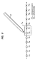
- the first drive pattern for the X conductors for determining the stylus position in track mode is schematically shown in FIG. 6.
- a base wire pair is defined as two adjacent conductors between which the stylus is believed to lie.
- adjacent conductors X6 and X7 are driven in three different patterns.
- the drive pattern is defined as PO.
- the drive pattern is identified as P2.
- FIG. 7 shows the amplitude of the signal received by the stylus 20 as it would pass from left to right from above the conductor X1 to a position above the conductor X12. Note that within and around the wire pair X6 and X7, the stylus signal varies somewhat linearly with position. The degree to which the signal strength curve approximates linearity depends in part on how far the stylus 20 is from the conductors. For this overlay, the signal strength curve is much less linear and any calculations based on linearity must be compensated. Also shown in FIG. 7 is the slight ripple in the signal strength curve over the driven conductors X7, X8, X9, X10, X11 and X12. The signal strength is slightly stronger directly over a driven conductor than it is between two driven conductors.
- the first phase in the locate mode is measuring the signal amplitude using drive pattern P0. Assuming that the stylus 20, is located somewhere between X6 and X7, the signal amplitude measured by the stylus 20 will be a single value along the sharp rise of the curve depicted in FIG. 7.
- the second pattern in the operation of tracking the position of the stylus 20 is shown in Fig. 8, where the drive pattern P2 is the inverse of the wire pair P0. That is, the conductors X1, X2, X3, X4, X5 and X6 are driven with the oscillator driver, whereas the conductors X7, X8, X9, X10, X11 and X12 are connected to ground or reference potential.
- the signal amplitude as the stylus 20 moves from left to right across the conductors is shown for the drive pattern P2 in FIG. 7.
- the stylus 20 is in the same position as for FIGs.
- the magnitude of the signal for the wire pair P2 will be measured somewhere along the sharp fall between conductors X6 and X7 as shown in FIG. 8. Similar to FIG. 7, there is a ripple in signal strength over the driven conductors X1, X2, X3, X4, X5 and X6. As the stylus 20 gets closer to the conductors in the overlay 16, the ripple over the driven conductors becomes more accentuated and the rise or fall in the signal strength between conductors X6 and X7 becomes less linear.
- FIG. 9 depicts the signal strength curve which would be measured as the stylus 20 is moved across the overlay 16 from X1 to X12.
- the curve is bimodal with the two modes occurring directly over the driven conductors and the closer the stylus is to the overlay the more pronounced the bimodal nature becomes. Since the PX patterns only drive two conductors, the electric field above the surface more non-uniform in the X and y directions of the sensor and the stylus signals show larger variations with lateral motion.
- FIG. 10 depicts the fourth drive pattern in the track mode where all the X and Y conductors in the overlay are driven simultaneously for contact detection. While other drive patterns could be used for stylus detection, driving all the conductors creates the most uniform signal across the overlay. This pattern is used to evaluate the height of the stylus above the display surface and is distinct from the other patterns of the track mode in that conductors far from the base position are driven. By driving all of the conductors, very accurate height determination is possible as the electrical field varies very slightly with lateral position as can be seen in FIG. 10.
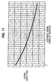
- FIG. 11 depicts the relationship between signal amplitude and distance from the overlay surface. If the signal amplitude is less than predicted for contact with the touch overlay surface, the sensed positions are not recorded as contact points, but as proximity points by the improved stylus sensing system.
- the figure depicts signal amplitude over a single point in the overlay as the signal amplitude is strongest where the conductors are closest to the electrical bus and weakest at the conductors termination furthest away from the bus.
- the next three drive patterns are essentially the same as depicted in FIGS. 7, 8 and 9, but for the conductors, for example, Y1, Y2,...Y12.
- Y6 and Y7 are the two conductors between which the stylus is located and around which drive patterns PO, P2 and PX for the Y conductors.
- the locate and tracking mode of stylus has determined the base position of the stylus.
- the base position is defined as the central point between the two X conductors and the two Y conductor between which the stylus is located. In the preceding FIGs., the base position is the central point between X conductors X6 and X7 and Y conductors Y6 and Y7 on the overlay.
- a series of compensation or calibration steps are taken to account the nonlinear nature of the signal strengths for the various drive patterns across the overlay. These calibration steps are derived empirically for a particular overlay and stylus combination, although the values in the tables might be theoretically calculated. Those skilled in the art will appreciate that other calibration methods may be possible.
- the offset to the base position is calculated in both X and Y directions.
- the offset of the stylus relative to base position is calculated with the signal values collected during the PO, P2, PX operations for each axis.
- the square area bounded by conductors X6, X7, Y6 and Y7 is called the base region.
- the base region is divided into 32 sections, so an offset from -16 to +16 is reported.
- the offset is non-linear function of the PO, P2, and PX values.
- the offset generated by the above equation is 1/64 of a wire distance, twice the reportable density.
- the compensation table for the X and Y positions is a one dimension vector with 64 values which corrects for nonlinearity in the offset calculation and converts to an offset from -16 to +16. If the offset is calculated by the above equation to be +28, the system will look at the 60th value in the vector. The vector may indicate that the stylus is really on offset 13 rather than 28, so the value of 13 is substituted into the equation to determine the coordinate value.
- the referenced patent does not compensate for the nonlinearities in the offset calculation. These nonlinearities are due to the shapes of the signal strength curves PX, PO, and P2 as a function of offset location. Although the compensation is performed using a table, one could develop an equation to perform this function.
- the nonlinearity in the dual drive mode used for contact detection is illustrated by the three dimensional diagram in FIG. 12.
- the vertical dimension depicts signal amplitude and the two horizontal axes depict the -16 to +16 offset divisions.
- the weakest signal is measured at the base position and the strongest signal is measured where the conductors cross.
- the strength of the stylus altitude signal has been found to be not only a function of the altitude, but also the X and Y delta from the base location i.e., the location between the transparent conductors. While the variations are not as great with the Dual Drive signal discussed above as it was with the prior art, further improvements in contact detection accuracy are achieved using the 2 dimensional compensation table.
- the offset compensation table is a function of the stylus geometry and overlay geometry and is shown below.
- the relative stylus altitude is computed from the dual drive value collected in the middle of the drive sequence. Since the measurement value has a small dependence on the X, Y location as well as altitude, it is also corrected by using a 2 dimensional (X,Y) compensation table. Using the adjusted signal strength value and the value in the 2 dimensional compensation table, based on current stylus position the final adjusted signal strength is found with the following equation:
- the final signal strength value is compared to a "contact” threshold. If the value exceeds the threshold, the coordinates generated for that cycle are tagged “in contact” coordinates. Otherwise they are tagged “proximity” coordinates.
- the coordinates, the tag and the corrected amplitude are passed to the computer system.
- FIG. 13 shows an architectural diagram of the improved detection system.
- the system depicted in FIG. 13 is very similar to that disclosed in the U.S. 4,686,332 patent in FIG. 2.
- the major differences include: the overlay 16 preferably has both X and Y conductor sets facing upward away from the display, the stylus 20 is of the improved design depicted in FIG. 4, the touch control processor 100, random access memory 102, read only memory 104 and the I/O controller 106 are on a touch panel adapter card 107 in a personal computer while the rest of the touch electronics are integrated in the touch workpad 10.
- the touch workpad 10 communicates with the personal computer and touch panel adapter card via cable 28.
- the vertical conductors X1-X112 are connected through the X bus 80 to the wire select multiplexer 112 and the horizontal Y conductors Y1-Y112 are connected through the Y bus 90 to the wire selection multiplexer 112.
- the radiative pickup stylus 20 is connected through the gate 120 to the radiative pickup measurement device 122.
- the wire selection multiplexer 112 is connected through the mode multiplexer 116 to the capacitance measurement device 128 which is used for capacitance finger touch detection.
- the wire selection multiplexer 112 is also connected through the mode multiplexer 116 to the 40 kilohertz oscillator driver 126 which is used to drive the X bus 80 and the Y bus 90 for the stylus detection operation.
- the mode multiplexer 116 also has an enabling output to the gate 120 to selectively connect the output of the stylus 20 to the radiative pickup measurement device 122, for stylus detection operations.
- the output of the capacitance measurement device is connected through the analog-to-digital converter 130 to the workpad bus 110.
- the output of the radiative pickup measurement device 122 is connected through the analog-to-digital converter 124 to the bus 110.
- a control input 114 to the wire selection multiplexer 112 is connected to the bus 110 and the control input 118 to the mode multiplexer 116 is connected to the bus 110.
- the workpad bus 110 is connected via workpad interface 111 to the cable 28 which connects to PC interface 113 in the touch panel adapter card 107 in the personal computer.
- the PC interface 113 communicates to the main system bus 115 and to the adapter card bus 117.
- the I/O controller 106 has an I/O bus 108 which connects to the main 115 bus of the Personal Computer.
- the I/O controller 106 is also connected to adapter card bus 117.
- the bus 117 also interconnects the control processor 100 with the read only memory (ROM) 104, and the random access memory (RAM) 102.
- the personal computer includes standard devices such as a CPU 132, ROM 134, disk storage 136, a memory 138 which stores operating system 140 and application program 142, a keyboard 144 and display 146.
- the wire selection multiplexer 112 and the mode multiplexer 116 connects selected patterns of a plurality of the horizontal and vertical conductors in the overlay 20 to either the capacitance measurement device 128 or the 40 kilohertz oscillator driver 126, in response to control signals applied over the control inputs 114 and 118 from the bus 110 by the control processor 100.
- the capacitance measuring device 128 has its input coupled through the mode multiplexer 116 and the wire selection multiplexer 112 to selected ones of the horizontal and vertical conductors in the overlay 16 in response to control signals from the control processor 100.
- the output of the capacitance measurement device 128 is converted to digital values by the converter 130 and is supplied over the bus 110 to the control processor 100, which executes a sequence of stored program instructions to detect the horizontal array conductor pair and the vertical array conductor pair in the overlay 16 which are being touched by the operator's finger.
- the 40 kilohertz output of the oscillator driver 126 is connected through the mode multiplexer 116 and the wire selection multiplexer 112 to selected ones of the conductors in the overlay 16, in response to control signals applied over the control inputs 114 and 118 from the control processor 100.
- the electromagnetic signals received from the overlay 16 by the stylus 20 are passed through the gate 120 to the radiative pickup measurement device 122, which measures those signals and provides an output which is digitized by the converter 124 and output to the control processor 100.
- the control processor 100 executes a sequence of stored program instructions to detect the proximity of the stylus to the overlay 16 in the proximity detection mode and then to locate and track the horizontal and vertical position of the stylus with respect to the overlay 16 in the location and tracking mode.
- the stored program instructions for carrying out these operations can be stored in the read only memory 104 and/or the RAM 102, for execution by the control processor 100. Positional values and other result information can be output through the I/O controller 106 on the I/O bus 108 to the host processor for further analysis and use in applications software.
- FIG. 14 is a flow diagram of a the preferred embodiment of the invention where either finger touch operations or alternately stylus detection operations can be carried out. It has been found that there are very few circumstances in which a user wants to carry out finger touch operations to the exclusion of stylus detection when the stylus is proximate to the overlay. On the other hand, much of the time a user will rest his hand on the overlay while writing with the stylus so the capacitance changes in the overlay due to the user's hand must be excluded while the stylus is sensed.
- Idle mode is the mode in which the sensing system is typically placed by the controller processor 100.
- Appropriate control messages are sent to the wire select multiplexer 112 to drive all X and Y conductors via the X-bus 80 and Y-bus 90 and to the mode multiplexer 116 to send all radiative signals captured by the stylus 20 back to the control processor 100 through the gate 120 radiative pickup measurement device 122 and A/D converter 124.
- the mode multiplexer 116 also connects the 40 kilohertz oscillator 126 to the overlay 16 through the wire select multiplexer 112.
- step 202 If a signal amplitude above the finger sense exclusion threshold is sensed in step 202, stylus detection steps 204 through 218 are attempted. If the signal amplitude is below the threshold, finger sense steps 220 through 228 are attempted.
- the sensing system transfers to stylus locate mode in step 204.
- locate mode the control processor 100 sends the appropriate control messages to the wire select multiplexer 112 to selectively connect each of the X and Y conductors to the 40 kilohertz oscillator 16 in the locate driver pattern.
- the signals received by the stylus 20 are sent back to the control processor 100 in an attempt to identify the two conductors in both X and Y planes which return the highest signal amplitude, and therefore, the conductors which are closest to the stylus 20.
- the control processor 100 is successful in locating the stylus 20 over a predetermined number of locate scans in step 206, the stylus sensing system passes into track mode in steps 208 through 216. If the stylus is not located in step 206, the sensing system returns to idle mode, step 200.
- the wire select multiplexer 112 receives control messages from the control processor 100 to drive the twelve X conductors closest to the stylus 20 in the drive patterns depicted in FIGs. 7, 8 and 9 in step 208.
- step 209 all the conductors are coupled to the oscillator 126 to determine whether the stylus 20 is contact with the overlay 16 as described in conjunction with FIGs. 10 and 11.
- the wire select multiplexer 112 then receives control messages to drive the twelve Y conductors closest to the stylus 20 in drive patterns analogous to those depicted in FIGs. 7, 8, and 9 in step 210.
- the signal amplitudes received by the stylus 20 are sent back to the control processor 100.
- step 212 the PO, P2, PX and Altitude signals are evaluated to determine whether the stylus 20 was in contact with overlay 16, the calculated stylus position is compensated by the above mentioned calibration tables to correct for the nonlinearity of the electrical field over the overlay 16 in step 214.
- the measurement step 209 is compensated for nonlinearity.
- the calibrated pen point is output by the control processor along bus 117 either to RAM 102 for storage or to I/O controller 106 for output to the personal computer along the I/O bus 108.
- the system goes back to step 208 to track the next stylus position.
- the stylus 20 was not in contact with the overlay 16, the stylus position is reported by the control processor 100 as a proximity point in step 218.
- Proximity information is of use to application programs run on the personal computer which are aware of the workings of the stylus sensing positions. After the proximity point is reported, the system returns to locate mode in step 204.
- step 202 If the signal amplitude received by the stylus is not above the finger sense exclusion threshold in step 202, the system passes into sense mode to determine whether a finger has touched the overlay 16.
- the sense mode described below is similar from that disclosed in the 4,686,332 patent.
- the wire select multiplexer 112 and the mode multiplexer 116 receive appropriate control signals from the control processor 100 to begin scanning all conductors for a change in capacitance indicating the presence of a finger. In response to these signals, the wire select multiplexer 112 begin connecting selected X and Y conductors to the capacitive measurement device 128 which has been connected by the mode multiplexer 116.
- the mode multiplexer 116 also disconnects the 40KHz oscillator 126, and therefore no signals can be picked up by the stylus. If the finger touch is located in step 222 by the change in capacitance in a particular area of the overlay 16, the system goes on to a more precise scan in step 224 of the area the overlay 16 to locate the finger touch. The change in capacitance values are set back to the control processor 100 via the A/D converter 130. The finger position is output by the control processor 100 along bus 117 either to the RAM 102 or I/O controller 106. At this point, the system returns to idle mode 100.
- the average values for the ambient capacitance of the overlay are updated, step 228, and the system returns to idle mode 200.
- the ambient capacitance drifts somewhat with temperature, video image and other factors.
- An updated average ambient capacitance is kept to determine whether any measured difference in capacitance is due to a finger touchdown on the overlay.
- electrostatic electrostatic
- electromagnetic electromagnetic field strength
Applications Claiming Priority (2)
| Application Number | Priority Date | Filing Date | Title |
|---|---|---|---|
| US608062 | 1990-10-31 | ||
| US07/608,062 US5117071A (en) | 1990-10-31 | 1990-10-31 | Stylus sensing system |
Publications (2)
| Publication Number | Publication Date |
|---|---|
| EP0483709A2 true EP0483709A2 (fr) | 1992-05-06 |
| EP0483709A3 EP0483709A3 (en) | 1993-03-17 |
Family
ID=24434864
Family Applications (1)
| Application Number | Title | Priority Date | Filing Date |
|---|---|---|---|
| EP19910118305 Withdrawn EP0483709A3 (en) | 1990-10-31 | 1991-10-27 | Improved stylus sensing system |
Country Status (3)
| Country | Link |
|---|---|
| US (1) | US5117071A (fr) |
| EP (1) | EP0483709A3 (fr) |
| JP (1) | JPH0727434B2 (fr) |
Cited By (11)
| Publication number | Priority date | Publication date | Assignee | Title |
|---|---|---|---|---|
| FR2704340A1 (fr) * | 1993-04-20 | 1994-10-28 | Samsung Display Devices Co Ltd | Numériseur. |
| EP0915429A2 (fr) * | 1997-11-04 | 1999-05-12 | Wacom Co., Ltd. | Méthode de détection de position et appareil pour détecter plusieurs indicateurs de position |
| DE19514651B4 (de) * | 1994-04-21 | 2009-08-06 | Samsung Display Devices Co., Ltd. | Informationseingabevorrichtung, welche sowohl als Berührungstablett als auch als Digitalisiertablett funktioniert, sowie ein Verfahren zum Betreiben dieser Informationseingabevorrichtung |
| WO2012076637A1 (fr) * | 2010-12-08 | 2012-06-14 | Trw Automotive Electronics & Components Gmbh | Procédé de détection d'une position d'un effleurement sur une zone tactile capacitive |
| WO2013037103A1 (fr) * | 2011-09-13 | 2013-03-21 | Tsai Hsiung-Kuang | Système d'interface visuelle |
| EP2315109A3 (fr) * | 2009-10-23 | 2014-09-10 | LG Electronics Inc. | Terminal mobile |
| US8917253B2 (en) | 2012-08-31 | 2014-12-23 | Blackberry Limited | Method and apparatus pertaining to the interlacing of finger-based and active-stylus-based input detection |
| EP2818991A1 (fr) * | 2013-06-28 | 2014-12-31 | Samsung Electronics Co., Ltd | Appareil électronique et son procédé de détection tactile |
| ITRM20130579A1 (it) * | 2013-10-21 | 2015-04-22 | Prb S R L | Metodo per l¿acquisizione della firma naturale per mezzo di tavoletta digitalizzatrice del tipo ¿touch screen¿. |
| TWI492110B (zh) * | 2011-09-13 | 2015-07-11 | Hsiung Kuang Tsai | 視覺介面系統 |
| EP2290510B1 (fr) * | 2009-08-27 | 2018-07-04 | BlackBerry Limited | Affichage sensible au toucher doté de capteurs tactiles capacitifs et résistifs et procédé de commande |
Families Citing this family (123)
| Publication number | Priority date | Publication date | Assignee | Title |
|---|---|---|---|---|
| US6491225B1 (en) * | 1989-10-30 | 2002-12-10 | Symbol Technologies, Inc. | Electro-optical reader with electronic stylus |
| JPH0769767B2 (ja) * | 1991-10-16 | 1995-07-31 | インターナショナル・ビジネス・マシーンズ・コーポレイション | フィンガ・タッチまたはスタイラスの位置を検出するためのタッチ・オーバーレイ、および検出システム |
| JPH05158606A (ja) * | 1991-12-05 | 1993-06-25 | Wacom Co Ltd | 位置検出装置のセンス部及びその製造方法 |
| US5673066A (en) * | 1992-04-21 | 1997-09-30 | Alps Electric Co., Ltd. | Coordinate input device |
| US5889236A (en) * | 1992-06-08 | 1999-03-30 | Synaptics Incorporated | Pressure sensitive scrollbar feature |
| DE69324067T2 (de) * | 1992-06-08 | 1999-07-15 | Synaptics Inc | Objekt-Positionsdetektor |
| US5942733A (en) * | 1992-06-08 | 1999-08-24 | Synaptics, Inc. | Stylus input capacitive touchpad sensor |
| US6028271A (en) * | 1992-06-08 | 2000-02-22 | Synaptics, Inc. | Object position detector with edge motion feature and gesture recognition |
| US5880411A (en) | 1992-06-08 | 1999-03-09 | Synaptics, Incorporated | Object position detector with edge motion feature and gesture recognition |
| US6239389B1 (en) | 1992-06-08 | 2001-05-29 | Synaptics, Inc. | Object position detection system and method |
| US7532205B2 (en) | 1992-06-08 | 2009-05-12 | Synaptics, Inc. | Object position detector with edge motion feature and gesture recognition |
| KR940001227A (ko) * | 1992-06-15 | 1994-01-11 | 에프. 제이. 스미트 | 터치 스크린 디바이스 |
| US5349139A (en) * | 1992-10-30 | 1994-09-20 | International Business Machines | Architecture for communication of remote devices to a digitizing display |
| JP2986047B2 (ja) * | 1993-04-29 | 1999-12-06 | インターナショナル・ビジネス・マシーンズ・コーポレイション | ディジタル入力用表示装置並びに入力処理装置および方法 |
| US5414227A (en) * | 1993-04-29 | 1995-05-09 | International Business Machines Corporation | Stylus tilt detection apparatus for communication with a remote digitizing display |
| US5475401A (en) * | 1993-04-29 | 1995-12-12 | International Business Machines, Inc. | Architecture and method for communication of writing and erasing signals from a remote stylus to a digitizing display |
| GB9406702D0 (en) * | 1994-04-05 | 1994-05-25 | Binstead Ronald P | Multiple input proximity detector and touchpad system |
| GB9422911D0 (en) * | 1994-11-14 | 1995-01-04 | Moonstone Technology Ltd | Capacitive touch detectors |
| FI103837B1 (fi) * | 1994-12-22 | 1999-09-30 | Nokia Mobile Phones Ltd | Tiedonsiirto- ja käsittelymenetelmä |
| US5823782A (en) * | 1995-12-29 | 1998-10-20 | Tinkers & Chance | Character recognition educational system |
| USRE38286E1 (en) | 1996-02-15 | 2003-10-28 | Leapfrog Enterprises, Inc. | Surface position location system and method |
| USRE39881E1 (en) | 1996-02-15 | 2007-10-16 | Leapfrog Enterprises, Inc. | Surface position location system and method |
| US5854625A (en) * | 1996-11-06 | 1998-12-29 | Synaptics, Incorporated | Force sensing touchpad |
| ATE239869T1 (de) * | 1996-12-03 | 2003-05-15 | Elliott Energy Systems Inc | Elektrische anordnung für turbine/alternator auf gemeinsamer achse |
| GB9722766D0 (en) | 1997-10-28 | 1997-12-24 | British Telecomm | Portable computers |
| US7663607B2 (en) | 2004-05-06 | 2010-02-16 | Apple Inc. | Multipoint touchscreen |
| DE19856007A1 (de) * | 1998-12-04 | 2000-06-21 | Bayer Ag | Anzeigevorrichtung mit Berührungssensor |
| US6297811B1 (en) | 1999-06-02 | 2001-10-02 | Elo Touchsystems, Inc. | Projective capacitive touchscreen |
| US6504530B1 (en) | 1999-09-07 | 2003-01-07 | Elo Touchsystems, Inc. | Touch confirming touchscreen utilizing plural touch sensors |
| US6492979B1 (en) | 1999-09-07 | 2002-12-10 | Elo Touchsystems, Inc. | Dual sensor touchscreen utilizing projective-capacitive and force touch sensors |
| US6750978B1 (en) * | 2000-04-27 | 2004-06-15 | Leapfrog Enterprises, Inc. | Print media information system with a portable print media receiving unit assembly |
| US6661405B1 (en) | 2000-04-27 | 2003-12-09 | Leapfrog Enterprises, Inc. | Electrographic position location apparatus and method |
| US6668156B2 (en) | 2000-04-27 | 2003-12-23 | Leapfrog Enterprises, Inc. | Print media receiving unit including platform and print media |
| US6903730B2 (en) * | 2000-11-10 | 2005-06-07 | Microsoft Corporation | In-air gestures for electromagnetic coordinate digitizers |
| US6608618B2 (en) * | 2001-06-20 | 2003-08-19 | Leapfrog Enterprises, Inc. | Interactive apparatus using print media |
| US7916124B1 (en) | 2001-06-20 | 2011-03-29 | Leapfrog Enterprises, Inc. | Interactive apparatus using print media |
| US20030010544A1 (en) * | 2001-07-10 | 2003-01-16 | Ching-Chuan Chao | Low EMI digitizer tablet |
| US6727896B2 (en) * | 2001-08-01 | 2004-04-27 | Microsoft Corporation | Correction of alignment and linearity errors in a stylus input system |
| MXPA04007716A (es) * | 2002-02-06 | 2004-12-06 | Leapfrog Entpr Inc | Aparato y metodo interactivo de escritura. |
| US7058902B2 (en) * | 2002-07-30 | 2006-06-06 | Microsoft Corporation | Enhanced on-object context menus |
| US20040104890A1 (en) * | 2002-09-05 | 2004-06-03 | Leapfrog Enterprises, Inc. | Compact book and apparatus using print media |
| US20040063078A1 (en) * | 2002-09-30 | 2004-04-01 | Marcus Brian I. | Electronic educational toy appliance |
| US7352355B2 (en) * | 2002-10-28 | 2008-04-01 | Delphi Technologies, Inc. | Transparent overlay input device |
| US20040229195A1 (en) * | 2003-03-18 | 2004-11-18 | Leapfrog Enterprises, Inc. | Scanning apparatus |
| US7068262B2 (en) * | 2003-06-09 | 2006-06-27 | Leapfrog Enterprises, Inc. | Writing stylus for electrographic position location apparatus |
| US7265303B2 (en) * | 2003-12-17 | 2007-09-04 | Microsoft Corporation | Electromagnetic digitizer sensor array |
| US7995036B2 (en) | 2004-02-27 | 2011-08-09 | N-Trig Ltd. | Noise reduction in digitizer system |
| US20060127872A1 (en) * | 2004-03-17 | 2006-06-15 | James Marggraff | Method and device for associating a user writing with a user-writable element |
| US20060125805A1 (en) * | 2004-03-17 | 2006-06-15 | James Marggraff | Method and system for conducting a transaction using recognized text |
| US20060077184A1 (en) * | 2004-03-17 | 2006-04-13 | James Marggraff | Methods and devices for retrieving and using information stored as a pattern on a surface |
| US7453447B2 (en) * | 2004-03-17 | 2008-11-18 | Leapfrog Enterprises, Inc. | Interactive apparatus with recording and playback capability usable with encoded writing medium |
| US7831933B2 (en) | 2004-03-17 | 2010-11-09 | Leapfrog Enterprises, Inc. | Method and system for implementing a user interface for a device employing written graphical elements |
| US20060067576A1 (en) * | 2004-03-17 | 2006-03-30 | James Marggraff | Providing a user interface having interactive elements on a writable surface |
| US7853193B2 (en) * | 2004-03-17 | 2010-12-14 | Leapfrog Enterprises, Inc. | Method and device for audibly instructing a user to interact with a function |
| US20060033725A1 (en) * | 2004-06-03 | 2006-02-16 | Leapfrog Enterprises, Inc. | User created interactive interface |
| US7167675B2 (en) * | 2004-10-15 | 2007-01-23 | Leapfrog Enterprises, Inc. | Magnetic switch and apparatus including magnetic switch |
| US8050876B2 (en) * | 2005-07-18 | 2011-11-01 | Analog Devices, Inc. | Automatic environmental compensation of capacitance based proximity sensors |
| US7922099B1 (en) | 2005-07-29 | 2011-04-12 | Leapfrog Enterprises, Inc. | System and method for associating content with an image bearing surface |
| US7883420B2 (en) * | 2005-09-12 | 2011-02-08 | Mattel, Inc. | Video game systems |
| US20070087838A1 (en) * | 2005-09-12 | 2007-04-19 | Jonathan Bradbury | Video game media |
| US7936339B2 (en) * | 2005-11-01 | 2011-05-03 | Leapfrog Enterprises, Inc. | Method and system for invoking computer functionality by interaction with dynamically generated interface regions of a writing surface |
| US8067948B2 (en) | 2006-03-27 | 2011-11-29 | Cypress Semiconductor Corporation | Input/output multiplexer bus |
| US8144125B2 (en) * | 2006-03-30 | 2012-03-27 | Cypress Semiconductor Corporation | Apparatus and method for reducing average scan rate to detect a conductive object on a sensing device |
| TWI322374B (en) * | 2006-04-14 | 2010-03-21 | Ritdisplay Corp | Light transmission touch panel and manufacturing method thereof |
| US8279180B2 (en) * | 2006-05-02 | 2012-10-02 | Apple Inc. | Multipoint touch surface controller |
| CN104965621B (zh) | 2006-06-09 | 2018-06-12 | 苹果公司 | 触摸屏液晶显示器及其操作方法 |
| US8259078B2 (en) | 2006-06-09 | 2012-09-04 | Apple Inc. | Touch screen liquid crystal display |
| KR20110058895A (ko) | 2006-06-09 | 2011-06-01 | 애플 인크. | 터치 스크린 액정 디스플레이 |
| JP4838643B2 (ja) * | 2006-06-27 | 2011-12-14 | オプトレックス株式会社 | 入力装置付表示装置 |
| US8261967B1 (en) | 2006-07-19 | 2012-09-11 | Leapfrog Enterprises, Inc. | Techniques for interactively coupling electronic content with printed media |
| US8655258B2 (en) * | 2006-10-17 | 2014-02-18 | Vtech Electronics Ltd. | PC connectable electronic learning aid device with replaceable activity worksheets |
| US7948477B2 (en) * | 2006-12-15 | 2011-05-24 | Apple Inc. | PET-based touchpad |
| US8493330B2 (en) | 2007-01-03 | 2013-07-23 | Apple Inc. | Individual channel phase delay scheme |
| US9710095B2 (en) * | 2007-01-05 | 2017-07-18 | Apple Inc. | Touch screen stack-ups |
| JP4732376B2 (ja) * | 2007-02-09 | 2011-07-27 | 三菱電機株式会社 | タッチパネル及びタッチパネルを備えた液晶表示装置 |
| JP2009009249A (ja) * | 2007-06-26 | 2009-01-15 | Nissha Printing Co Ltd | 静電容量式タッチパネル及びこれを用いた2方式併用タッチパネル |
| US20090237373A1 (en) * | 2008-03-19 | 2009-09-24 | Sony Ericsson Mobile Communications Ab | Two way touch-sensitive display |
| JP5151808B2 (ja) * | 2008-08-27 | 2013-02-27 | コニカミノルタホールディングス株式会社 | 情報入力装置 |
| US8321174B1 (en) | 2008-09-26 | 2012-11-27 | Cypress Semiconductor Corporation | System and method to measure capacitance of capacitive sensor array |
| US8482545B2 (en) | 2008-10-02 | 2013-07-09 | Wacom Co., Ltd. | Combination touch and transducer input system and method |
| KR20100084252A (ko) * | 2009-01-16 | 2010-07-26 | 삼성모바일디스플레이주식회사 | 터치 스크린 패널 |
| US8279194B2 (en) * | 2009-05-22 | 2012-10-02 | Elo Touch Solutions, Inc. | Electrode configurations for projected capacitive touch screen |
| US20100295813A1 (en) * | 2009-05-22 | 2010-11-25 | Tyco Electronics Corporation | System and method for a projected capacitive touchscreen having grouped electrodes |
| JP2011028699A (ja) * | 2009-07-21 | 2011-02-10 | Touch Panel Kenkyusho:Kk | 静電容量式タッチパネル構造体 |
| US8477106B2 (en) * | 2009-07-29 | 2013-07-02 | Elo Touch Solutions, Inc. | System and method for a projected capacitive touchscreen having weight based coordinate determination |
| JP5442479B2 (ja) * | 2010-02-05 | 2014-03-12 | 株式会社ワコム | 指示体、位置検出装置及び位置検出方法 |
| KR20110102794A (ko) * | 2010-05-06 | 2011-09-19 | 삼성전기주식회사 | 터치스크린 및 이의 제어방법 |
| WO2011154950A1 (fr) | 2010-06-11 | 2011-12-15 | N-Trig Ltd. | Détection de l'orientation d'un objet à l'aide d'un numériseur |
| US9310923B2 (en) | 2010-12-03 | 2016-04-12 | Apple Inc. | Input device for touch sensitive devices |
| US8804056B2 (en) | 2010-12-22 | 2014-08-12 | Apple Inc. | Integrated touch screens |
| US8638320B2 (en) | 2011-06-22 | 2014-01-28 | Apple Inc. | Stylus orientation detection |
| US9329703B2 (en) | 2011-06-22 | 2016-05-03 | Apple Inc. | Intelligent stylus |
| US8928635B2 (en) | 2011-06-22 | 2015-01-06 | Apple Inc. | Active stylus |
| JP2013148941A (ja) * | 2012-01-17 | 2013-08-01 | Mitec:Kk | 静電容量式タッチパネル及びその生産方法 |
| US20130207926A1 (en) | 2012-02-15 | 2013-08-15 | Viktor Kremin | Stylus to host synchronization |
| CN102622128A (zh) * | 2012-02-24 | 2012-08-01 | 康佳集团股份有限公司 | 一种接近控制的方法及系统 |
| JP2012181866A (ja) * | 2012-05-21 | 2012-09-20 | Applied Vacuum Coating Technologies Co Ltd | タッチパッド構造 |
| US9176604B2 (en) | 2012-07-27 | 2015-11-03 | Apple Inc. | Stylus device |
| US9652090B2 (en) | 2012-07-27 | 2017-05-16 | Apple Inc. | Device for digital communication through capacitive coupling |
| US9557845B2 (en) | 2012-07-27 | 2017-01-31 | Apple Inc. | Input device for and method of communication with capacitive devices through frequency variation |
| US9158393B2 (en) | 2012-12-18 | 2015-10-13 | Logitech Europe S.A. | Active stylus for touch sensing applications |
| US20140168141A1 (en) | 2012-12-18 | 2014-06-19 | Logitech Europe S.A. | Method and system for discriminating stylus and touch interactions |
| US10048775B2 (en) | 2013-03-14 | 2018-08-14 | Apple Inc. | Stylus detection and demodulation |
| US9542046B2 (en) * | 2013-06-26 | 2017-01-10 | Atmel Corporation | Changing the detection range of a touch sensor |
| US9939935B2 (en) | 2013-07-31 | 2018-04-10 | Apple Inc. | Scan engine for touch controller architecture |
| CN104423756A (zh) * | 2013-09-09 | 2015-03-18 | 太瀚科技股份有限公司 | 触控面板控制方法 |
| US9477330B2 (en) * | 2013-11-05 | 2016-10-25 | Microsoft Technology Licensing, Llc | Stylus tilt tracking with a digitizer |
| US9298285B2 (en) * | 2013-12-05 | 2016-03-29 | Wacom Co., Ltd. | Stylus tip shape |
| US20150160851A1 (en) * | 2013-12-10 | 2015-06-11 | Kabushiki Kaisha Toshiba | Electronic device, method, and storage medium |
| US10061449B2 (en) | 2014-12-04 | 2018-08-28 | Apple Inc. | Coarse scan and targeted active mode scan for touch and stylus |
| US10095361B2 (en) | 2015-03-18 | 2018-10-09 | Microsoft Technology Licensing, Llc | Stylus detection with capacitive based digitizer sensor |
| US9720546B2 (en) | 2015-09-15 | 2017-08-01 | Microsoft Technology Licensing, Llc | Calibration of a force sensitive device |
| US10296146B2 (en) | 2015-12-22 | 2019-05-21 | Microsoft Technology Licensing, Llc | System and method for detecting grip of a touch enabled device |
| US10423268B2 (en) | 2015-12-22 | 2019-09-24 | Microsoft Technology Licensing, Llc | System and method for detecting grounding state of a touch enabled computing device |
| CN105677065B (zh) * | 2016-01-04 | 2019-01-01 | 京东方科技集团股份有限公司 | 用于显示屏的遥控触控装置及方法 |
| US9823774B2 (en) | 2016-02-23 | 2017-11-21 | Microsoft Technology Licensing, Llc | Noise reduction in a digitizer system |
| US10637933B2 (en) | 2016-05-26 | 2020-04-28 | Logitech Europe S.A. | Method and apparatus for transferring information between electronic devices |
| US10474277B2 (en) | 2016-05-31 | 2019-11-12 | Apple Inc. | Position-based stylus communication |
| US10540023B2 (en) | 2017-09-26 | 2020-01-21 | Yong Bum Kim | User interface devices for virtual reality system |
| US10509489B2 (en) | 2017-09-26 | 2019-12-17 | Yong Bum Kim | Systems and related methods for facilitating pen input in a virtual reality environment |
| US10678348B2 (en) | 2018-03-12 | 2020-06-09 | Microsoft Technology Licensing, Llc | Touch detection on an ungrounded pen enabled device |
| US10616349B2 (en) | 2018-05-01 | 2020-04-07 | Microsoft Technology Licensing, Llc | Hybrid sensor centric recommendation engine |
| US11562638B2 (en) | 2020-08-24 | 2023-01-24 | Logitech Europe S.A. | Electronic system and method for improving human interaction and activities |
Citations (3)
| Publication number | Priority date | Publication date | Assignee | Title |
|---|---|---|---|---|
| US4009338A (en) * | 1975-12-22 | 1977-02-22 | Ibm Corporation | Tablet with improved pen height compensation |
| US4473717A (en) * | 1982-02-08 | 1984-09-25 | Bausch & Lomb Incorporated | Digitizing system |
| US4686332A (en) * | 1986-06-26 | 1987-08-11 | International Business Machines Corporation | Combined finger touch and stylus detection system for use on the viewing surface of a visual display device |
Family Cites Families (11)
| Publication number | Priority date | Publication date | Assignee | Title |
|---|---|---|---|---|
| US3818133A (en) * | 1971-04-05 | 1974-06-18 | W Cotter | Coordinate digitizer incremental system |
| US3886311A (en) * | 1972-05-16 | 1975-05-27 | Talos Systems | Electrical writing pen and sensor |
| US3999012A (en) * | 1975-07-07 | 1976-12-21 | Ibm Corporation | Graphic entry tablet with improved addressing |
| JPS5627148A (en) * | 1979-08-11 | 1981-03-16 | Hokuetsu Seishi Kk | Reproduction proof paper for preparing master |
| US4423229A (en) * | 1980-11-18 | 1983-12-27 | The Upjohn Company | Composition of matter and process |
| JPS5987583A (ja) * | 1982-11-11 | 1984-05-21 | Sony Corp | 位置検出装置 |
| US4650926A (en) * | 1984-10-26 | 1987-03-17 | Scriptel Corporation | Electrographic system and method |
| US4678869A (en) * | 1985-10-25 | 1987-07-07 | Scriptel Corporation | Position responsive apparatus, system and method having electrographic application |
| JPS62184522A (ja) * | 1986-02-10 | 1987-08-12 | Alps Electric Co Ltd | 座標入力装置 |
| US4695680A (en) * | 1986-06-27 | 1987-09-22 | Scriptel Corporation | Stylus for position responsive apparatus having electrographic application |
| US4931782A (en) * | 1988-06-24 | 1990-06-05 | E. I. Du Pont De Nemours And Company | Touch screen overlay with improved conductor durability |
-
1990
- 1990-10-31 US US07/608,062 patent/US5117071A/en not_active Expired - Fee Related
-
1991
- 1991-10-22 JP JP3301335A patent/JPH0727434B2/ja not_active Expired - Fee Related
- 1991-10-27 EP EP19910118305 patent/EP0483709A3/en not_active Withdrawn
Patent Citations (3)
| Publication number | Priority date | Publication date | Assignee | Title |
|---|---|---|---|---|
| US4009338A (en) * | 1975-12-22 | 1977-02-22 | Ibm Corporation | Tablet with improved pen height compensation |
| US4473717A (en) * | 1982-02-08 | 1984-09-25 | Bausch & Lomb Incorporated | Digitizing system |
| US4686332A (en) * | 1986-06-26 | 1987-08-11 | International Business Machines Corporation | Combined finger touch and stylus detection system for use on the viewing surface of a visual display device |
Cited By (17)
| Publication number | Priority date | Publication date | Assignee | Title |
|---|---|---|---|---|
| FR2704340A1 (fr) * | 1993-04-20 | 1994-10-28 | Samsung Display Devices Co Ltd | Numériseur. |
| DE19514651B4 (de) * | 1994-04-21 | 2009-08-06 | Samsung Display Devices Co., Ltd. | Informationseingabevorrichtung, welche sowohl als Berührungstablett als auch als Digitalisiertablett funktioniert, sowie ein Verfahren zum Betreiben dieser Informationseingabevorrichtung |
| EP0915429A2 (fr) * | 1997-11-04 | 1999-05-12 | Wacom Co., Ltd. | Méthode de détection de position et appareil pour détecter plusieurs indicateurs de position |
| EP0915429A3 (fr) * | 1997-11-04 | 2000-04-19 | Wacom Co., Ltd. | Méthode de détection de position et appareil pour détecter plusieurs indicateurs de position |
| EP2290510B1 (fr) * | 2009-08-27 | 2018-07-04 | BlackBerry Limited | Affichage sensible au toucher doté de capteurs tactiles capacitifs et résistifs et procédé de commande |
| EP2315109A3 (fr) * | 2009-10-23 | 2014-09-10 | LG Electronics Inc. | Terminal mobile |
| WO2012076637A1 (fr) * | 2010-12-08 | 2012-06-14 | Trw Automotive Electronics & Components Gmbh | Procédé de détection d'une position d'un effleurement sur une zone tactile capacitive |
| US9342197B2 (en) | 2010-12-08 | 2016-05-17 | Trw Automotive Electronics & Components Gmbh | Method for determining a position of a contact on a capacitive sensor field |
| CN103827934A (zh) * | 2011-09-13 | 2014-05-28 | 蔡熊光 | 电子装置及数据传输系统 |
| CN103797448A (zh) * | 2011-09-13 | 2014-05-14 | 蔡熊光 | 视觉界面系统 |
| EP2757444A4 (fr) * | 2011-09-13 | 2015-03-18 | Hsiung-Kuang Tsai | Système d'interface visuelle |
| TWI492110B (zh) * | 2011-09-13 | 2015-07-11 | Hsiung Kuang Tsai | 視覺介面系統 |
| WO2013037103A1 (fr) * | 2011-09-13 | 2013-03-21 | Tsai Hsiung-Kuang | Système d'interface visuelle |
| CN103797448B (zh) * | 2011-09-13 | 2018-09-04 | 祥闳科技股份有限公司 | 视觉界面系统 |
| US8917253B2 (en) | 2012-08-31 | 2014-12-23 | Blackberry Limited | Method and apparatus pertaining to the interlacing of finger-based and active-stylus-based input detection |
| EP2818991A1 (fr) * | 2013-06-28 | 2014-12-31 | Samsung Electronics Co., Ltd | Appareil électronique et son procédé de détection tactile |
| ITRM20130579A1 (it) * | 2013-10-21 | 2015-04-22 | Prb S R L | Metodo per l¿acquisizione della firma naturale per mezzo di tavoletta digitalizzatrice del tipo ¿touch screen¿. |
Also Published As
| Publication number | Publication date |
|---|---|
| US5117071A (en) | 1992-05-26 |
| JPH0727434B2 (ja) | 1995-03-29 |
| EP0483709A3 (en) | 1993-03-17 |
| JPH04266116A (ja) | 1992-09-22 |
Similar Documents
| Publication | Publication Date | Title |
|---|---|---|
| US5117071A (en) | Stylus sensing system | |
| US5149919A (en) | Stylus sensing system | |
| EP0250931B1 (fr) | Combinaison entre un écran tactile et la détection d'un style pour un appareil de visualisation | |
| US7030860B1 (en) | Flexible transparent touch sensing system for electronic devices | |
| US6961049B2 (en) | Capacitive touch sensor architecture with unique sensor bar addressing | |
| US11249638B2 (en) | Suppression of grip-related signals using 3D touch | |
| CN106155419B (zh) | 选择性地拒绝触摸表面的边缘区域中的触摸接触 | |
| US6762752B2 (en) | Dual function input device and method | |
| US7952564B2 (en) | Multiple-touch sensor | |
| US20140043289A1 (en) | Capacitive sensor for a digitizer system | |
| US20110134073A1 (en) | Touch panel device of digital capacitive coupling type with high sensitivity | |
| JPH05204546A (ja) | フィンガ・タッチまたはスタイラスの位置を検出するためのタッチ・オーバーレイ、および検出システム | |
| US20080100586A1 (en) | Method and system for calibrating a touch screen | |
| US20140098030A1 (en) | Touch module | |
| CN1675653A (zh) | 接触传感器 | |
| KR102111782B1 (ko) | 이엠알 터치 센서와 적외선 터치 센서를 갖는 좌표검출장치 | |
| AU2013100574A4 (en) | Interpreting touch contacts on a touch surface | |
| TWM241746U (en) | Touch-controlled input apparatus of electronic apparatus | |
| US20100309138A1 (en) | Position detection apparatus and method thereof | |
| CN109324700A (zh) | 可提供倾斜角与方位角侦测信号的电容笔 | |
| CN213987444U (zh) | 一种近眼显示设备的输入系统 | |
| Sherr | Input and Output | |
| CN109857283A (zh) | 自参考电容性力传感器 | |
| Ward et al. | Digitizer renaissance |
Legal Events
| Date | Code | Title | Description |
|---|---|---|---|
| PUAI | Public reference made under article 153(3) epc to a published international application that has entered the european phase |
Free format text: ORIGINAL CODE: 0009012 |
|
| AK | Designated contracting states |
Kind code of ref document: A2 Designated state(s): DE FR GB |
|
| PUAL | Search report despatched |
Free format text: ORIGINAL CODE: 0009013 |
|
| AK | Designated contracting states |
Kind code of ref document: A3 Designated state(s): DE FR GB |
|
| STAA | Information on the status of an ep patent application or granted ep patent |
Free format text: STATUS: THE APPLICATION IS DEEMED TO BE WITHDRAWN |
|
| 18D | Application deemed to be withdrawn |
Effective date: 19930918 |