EP0480697B1 - Tunable semiconductor laser - Google Patents
Tunable semiconductor laser Download PDFInfo
- Publication number
- EP0480697B1 EP0480697B1 EP91309258A EP91309258A EP0480697B1 EP 0480697 B1 EP0480697 B1 EP 0480697B1 EP 91309258 A EP91309258 A EP 91309258A EP 91309258 A EP91309258 A EP 91309258A EP 0480697 B1 EP0480697 B1 EP 0480697B1
- Authority
- EP
- European Patent Office
- Prior art keywords
- regions
- wavelength
- semiconductor laser
- electrode
- electrodes
- Prior art date
- Legal status (The legal status is an assumption and is not a legal conclusion. Google has not performed a legal analysis and makes no representation as to the accuracy of the status listed.)
- Expired - Lifetime
Links
Images


Classifications
-
- H—ELECTRICITY
- H01—ELECTRIC ELEMENTS
- H01S—DEVICES USING THE PROCESS OF LIGHT AMPLIFICATION BY STIMULATED EMISSION OF RADIATION [LASER] TO AMPLIFY OR GENERATE LIGHT; DEVICES USING STIMULATED EMISSION OF ELECTROMAGNETIC RADIATION IN WAVE RANGES OTHER THAN OPTICAL
- H01S5/00—Semiconductor lasers
- H01S5/06—Arrangements for controlling the laser output parameters, e.g. by operating on the active medium
- H01S5/062—Arrangements for controlling the laser output parameters, e.g. by operating on the active medium by varying the potential of the electrodes
- H01S5/0625—Arrangements for controlling the laser output parameters, e.g. by operating on the active medium by varying the potential of the electrodes in multi-section lasers
- H01S5/06255—Controlling the frequency of the radiation
- H01S5/06258—Controlling the frequency of the radiation with DFB-structure
-
- H—ELECTRICITY
- H01—ELECTRIC ELEMENTS
- H01S—DEVICES USING THE PROCESS OF LIGHT AMPLIFICATION BY STIMULATED EMISSION OF RADIATION [LASER] TO AMPLIFY OR GENERATE LIGHT; DEVICES USING STIMULATED EMISSION OF ELECTROMAGNETIC RADIATION IN WAVE RANGES OTHER THAN OPTICAL
- H01S5/00—Semiconductor lasers
- H01S5/10—Construction or shape of the optical resonator, e.g. extended or external cavity, coupled cavities, bent-guide, varying width, thickness or composition of the active region
- H01S5/12—Construction or shape of the optical resonator, e.g. extended or external cavity, coupled cavities, bent-guide, varying width, thickness or composition of the active region the resonator having a periodic structure, e.g. in distributed feedback [DFB] lasers
Definitions
- the present invention relates to a tunable distributed feedback semiconductor laser which has a wide tuning range and exhibits a narrow-linewidth characteristic.
- a distributed feedback (DFB) semiconductor laser with three electrodes has been studied for wavelength tuning and linewidth reduction.
- DFB distributed feedback
- An object of the present invention is to provide a wavelength-tunable semiconductor laser which has a wider tuning range and better linewidth characteristics than in the past.
- the electrode for current injection is split into four or more electrodes in the direction of the cavity, nonadjacent ones of them are electrically connected together to form two electrode groups so that the current injection to active layers in the regions corresponding to the respective electrodes can be made using the individual electrodes.
- These regions are divided into two groups of wavelength control regions and gain control regions respectively corresponding to the two electrode groups, and the both regions are arranged alternately with each other.
- each electrode and each region are set so that the total length of the wavelength control regions is larger than the total length of the gain control regions. It is preferred that the total length ratio of the wavelength control regions and the gain control regions is in the range of 5:1 to 5:4.
- the refractive index in each wavelength control region is changed through current injection change thereto to vary the lasing wavelength and the overall gain is held constant by controlling current injection to the gain control regions, by which it is possible to obtain output light of a constant output power and a variable single wavelength.
- the intensity of the output light also varies correspondingly, but the overall ain can be held constant through control of the injection current to the gain control regions by changing it with an increase or decrease in current in the wavelength control regions.
- wavelength control regions and the gain control regions are disposed dispersedly throughout the cavity of the laser, nonuniformity of parameters such as the refractive index and gain in the laser cavity is also effectively suppressed with respect to variations of the lasing wavelength, and consequently, the linewidth is less degraded.
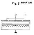
- a semiconductor laser that has been studied for wave-length tuning and linewidth reduction is a long cavity DFB (distributed feedback) semiconductor laser with three electrodes, such as shown in Fig. 3, and it has been reported that the semiconductor laser exhibits a maximum continuous tuning range of 1.9 nm and a minimum linewidth of 550 kHz ("TUNABLE, NARROW-LINEWIDTH AND HIGH-POWFR ⁇ /4-SHIFTED DFB LASER,” ELECTRONICS LETTERS, 20th July 1989, Vol. 25, No. 15, pp990-992).
- DFB distributed feedback
- the hole burning effect is controlled by controlling a ratio of a current Ic of a center portion to a current Is of side portions to vary the threshold carrier density, thus achieving wavelength tuning.
- the light source at the transmitting side and the light source employed as a local oscillator at the receiving side be narrow in linewidth and variable in oscillation wavelength, and their linewidth is required to remain narrow irrespective of wavelength variations.
- the wavelength tuning range is not so wide as aimed at, because of a limit to the variation in the carrier density by suppression of the hole burning effect.
- Fig. 1 illustrates an embodiment of the present invention.
- reference numeral 1 indicates an n-type InP substrate, 2 an n-type InGaAsP waveguide layer, 3 an InGaAsP active layer, 4 an InGaAsP buffer layer and 5 a diffraction grating having a quarter-wavelength phase shift point 6 at the center thereof.
- the active layer 3 is divided into five regions 7, 8, 9, 10 and 11 along the direction of travel of light, and electrodes 12, 13, 14, 15 and 16 are formed on the respective regions.
- the electrodes 12, 14 and 16 are electrically interconnected to form a first electrode group, whereas the electrodes 13 and 15 are electrically interconnected to form a second electrode group.
- the lengths of the regions 7, 8, 9, 10 and 11 are 225 ⁇ m, 100 ⁇ m, 150 ⁇ m, 100 ⁇ m and 225 ⁇ m, respectively, and the total cavity length is 800 ⁇ m.
- Reference numerals 17, 18, 19 and 20 denote high resistance regions for electrical isolation, which can be formed by implantation of proton and so on.
- Reference numeral 21 identifies an n-side electrode. In the vicinities of both facets there are provided window structures 22 and 23 for preventing reflection from the facets.
- the regions 7, 9 and 11 are wavelength control regions and the regions 8 and 10 are gain control regions.
- the ratio in length between the both regions is about 3:1.
- Fig. 2 illustrates another embodiment of the present invention.
- This embodiment is identical in structure with that shown in Fig. 1 except that no diffraction grating is provided in each gain control region, and the mechanisms for wavelength tuning and gain control are also the same as those in the embodiment of Fig. 1.
- the refractive index of the region When the current to gain control region is changed for gain control, the refractive index of the region also varies, but since the region has no diffraction grating in this structure, the refractive index variation will not cause any disturbance to the lasing wavelength. Accordingly, this embodiment can be expected to achieve more stable single-wavelength operation and wider tuning range.
- the lasing wavelength is greatly deviated from ⁇ , then unbalance between the amounts of injection currents increases accordingly, but by employing a structure in which, for example, the length per unit region is further reduced to increase the number of regions for further homogenization of the refractive index and other parameters in the cavity, the effective cavity length can be held substantially constant, and hence deterioration of the linewidth can be prevented. Accordingly, in these embodiments, though described to have five electrodes (i.e. regions), as the number of electrodes increases in excess of at least four, the intra-cavity homogeneity of such parameters as the refractive index and gain improves.
- the linewidth can be made narrower by making the overall cavity length longer.
- a narrow-linewidth device can be obtained by introducing such a quantum effect as MQW or the like into the light emitting layer.
- optical waveguide structure all waveguide structures, including a buried structure, can be employed.
- the present invention can be used not only with those of the aforementioned InGaAsP/InP systems but also with other semiconductor materials of InAlGaAs/InP, AlGaAs/GaAs systems and so forth.
- a semiconductor laser which is continuously tunable, has a wide tuning range and a narrow linewidth uniformly over the entire tuning range and can be used as a single-wavelength light source.
- Embodiments of the tunable semiconductor laser according to the invention can be expected, theoretically, to achieve a continuous tuning range of 5 nm or more and a linewidth below 500 kHz.
- An embodiment of the tunable semiconductor laser in which the periodic corrugations are not formed on any of the active layers and layers adjacent to said active layers of the gain control regions can be expected to achieve a more stable single-wavelength operation and a wider tuning range.
- the semiconductor laser according to the present invention is very promising as a light source for coherent transmission, optical measurements, etc., and hence is of great utility.
Landscapes
- Physics & Mathematics (AREA)
- Condensed Matter Physics & Semiconductors (AREA)
- General Physics & Mathematics (AREA)
- Electromagnetism (AREA)
- Optics & Photonics (AREA)
- Semiconductor Lasers (AREA)
Description
- The present invention relates to a tunable distributed feedback semiconductor laser which has a wide tuning range and exhibits a narrow-linewidth characteristic.
- A distributed feedback (DFB) semiconductor laser with three electrodes has been studied for wavelength tuning and linewidth reduction. However, it has not been realized to obtain a wave-length-tunable distributed feedback semiconductor laser which has necessarily and sufficiently a wide tuning range and a narrow line width.
- An object of the present invention is to provide a wavelength-tunable semiconductor laser which has a wider tuning range and better linewidth characteristics than in the past.
- According to the present invention there is provided a distributed feedback semiconductor laser according to
claim 1. - That is, according to the present invention, in the distributed feedback semiconductor laser (hereinafter referred to as a DFB laser) which can be expected to exhibit an excellent single-wavelength lasing characteristic even in case of high-speed modulation, the electrode for current injection is split into four or more electrodes in the direction of the cavity, nonadjacent ones of them are electrically connected together to form two electrode groups so that the current injection to active layers in the regions corresponding to the respective electrodes can be made using the individual electrodes. These regions are divided into two groups of wavelength control regions and gain control regions respectively corresponding to the two electrode groups, and the both regions are arranged alternately with each other. In this instance, the lengths of each electrode and each region are set so that the total length of the wavelength control regions is larger than the total length of the gain control regions. It is preferred that the total length ratio of the wavelength control regions and the gain control regions is in the range of 5:1 to 5:4. The refractive index in each wavelength control region is changed through current injection change thereto to vary the lasing wavelength and the overall gain is held constant by controlling current injection to the gain control regions, by which it is possible to obtain output light of a constant output power and a variable single wavelength.
- Uniform current injection to the DFB laser will provide output light of a wavelength λ₀, which is given by λ₀ = 2Λn, where Λ is the period of the diffraction grating and n is the refractive index of the light emitting layer. Since the refractive index n can be varied with the carrier density in the light emitting layer through utilization of the plasma effect, it has been found that the lasing wavelength varies with the change of the refractive index.
- In the above-described structure in which the total length of the wavelength control regions is larger than the total length of the gain control regions, when the refractive index of the wavelength control region is changed to n′ by changing the current injection thereto, the change in the refractive index of the wavelength control region governs the overall lasing wavelength, which varies to a wavelength λ′ given by λ′ = 2Λn′. On the other hand, the intensity of the output light also varies correspondingly, but the overall ain can be held constant through control of the injection current to the gain control regions by changing it with an increase or decrease in current in the wavelength control regions.
- Moreover, since the wavelength control regions and the gain control regions are disposed dispersedly throughout the cavity of the laser, nonuniformity of parameters such as the refractive index and gain in the laser cavity is also effectively suppressed with respect to variations of the lasing wavelength, and consequently, the linewidth is less degraded.
- Embodiments of the present invention will be described in detail below by way of example in comparison with prior art and with reference to the accompanying drawings, in which:
- Fig. 1 is a cross-sectional view illustrating a semiconductor laser of an embodiment according to the present invention;
- Fig. 2 is a cross-sectional view illustrating a semi-conductor laser of another embodiment according to the present invention; and
- Fig. 3 is a cross-sectional view of a conventional narrow-linewidth, tunable semiconductor laser.
- To make differences between prior art and the present invention clean, an example of prior art will first be described.
- A semiconductor laser that has been studied for wave-length tuning and linewidth reduction is a long cavity DFB (distributed feedback) semiconductor laser with three electrodes, such as shown in Fig. 3, and it has been reported that the semiconductor laser exhibits a maximum continuous tuning range of 1.9 nm and a minimum linewidth of 550 kHz ("TUNABLE, NARROW-LINEWIDTH AND HIGH-POWFR λ/4-SHIFTED DFB LASER," ELECTRONICS LETTERS, 20th July 1989, Vol. 25, No. 15, pp990-992).
- With the illustrated structure, the hole burning effect is controlled by controlling a ratio of a current Ic of a center portion to a current Is of side portions to vary the threshold carrier density, thus achieving wavelength tuning.
- In coherent transmission systems which can be expected to lengthen a repeater spacing and increase a line capacity as compared with conventional transmitting systems, it is indispensable that the light source at the transmitting side and the light source employed as a local oscillator at the receiving side be narrow in linewidth and variable in oscillation wavelength, and their linewidth is required to remain narrow irrespective of wavelength variations.
- In such a prior art wavelength-tunable semiconductor laser as shown in Fig. 3, which is operated by controlling the hole burning effect in the central portion, however, the wavelength tuning range is not so wide as aimed at, because of a limit to the variation in the carrier density by suppression of the hole burning effect. Furthermore, to enlarge the wavelength tuning range closely to its limit, it is necessary to substantially vary the ratio of the current of the center portion to the current of the side portions. With large variation of the current ratio, however, the carrier density and the distribution of refractive index in the laser become appreciably nonuniform in the direction of travel of light, resulting in an increased linewidth. Accordingly, it is impossible to obtain a wavelength-tunable semiconductor laser which has necessarily and sufficiently, a wide tuning range and a narrow linewidth.
- Another tunable DFB laser, consisting of two groups of regions with common electrodes, is disclosed in DE-A-3706866.
- The present invention will now be described.
- Fig. 1 illustrates an embodiment of the present invention. In Fig. 1,
reference numeral 1 indicates an n-type InP substrate, 2 an n-type InGaAsP waveguide layer, 3 an InGaAsP active layer, 4 an InGaAsP buffer layer and 5 a diffraction grating having a quarter-wavelengthphase shift point 6 at the center thereof. Theactive layer 3 is divided into fiveregions electrodes electrodes electrodes regions Reference numerals Reference numeral 21 identifies an n-side electrode. In the vicinities of both facets there are providedwindow structures - In this embodiment the
regions 7, 9 and 11 are wavelength control regions and theregions 8 and 10 are gain control regions. The ratio in length between the both regions is about 3:1. As described previously, it is possible to vary the lasing wavelength by changing a current I₁ which is injected to the wavelength control regions and to maintain the overall gain constant by controlling a current I₂ which is injected to the gain control regions. - Fig. 2 illustrates another embodiment of the present invention. This embodiment is identical in structure with that shown in Fig. 1 except that no diffraction grating is provided in each gain control region, and the mechanisms for wavelength tuning and gain control are also the same as those in the embodiment of Fig. 1. When the current to gain control region is changed for gain control, the refractive index of the region also varies, but since the region has no diffraction grating in this structure, the refractive index variation will not cause any disturbance to the lasing wavelength. Accordingly, this embodiment can be expected to achieve more stable single-wavelength operation and wider tuning range.
- If the lasing wavelength is greatly deviated from λ, then unbalance between the amounts of injection currents increases accordingly, but by employing a structure in which, for example, the length per unit region is further reduced to increase the number of regions for further homogenization of the refractive index and other parameters in the cavity, the effective cavity length can be held substantially constant, and hence deterioration of the linewidth can be prevented. Accordingly, in these embodiments, though described to have five electrodes (i.e. regions), as the number of electrodes increases in excess of at least four, the intra-cavity homogeneity of such parameters as the refractive index and gain improves.
- The linewidth can be made narrower by making the overall cavity length longer.
- Moreover, a narrow-linewidth device can be obtained by introducing such a quantum effect as MQW or the like into the light emitting layer.
- While in the above no particular reference is made to the optical waveguide structure, all waveguide structures, including a buried structure, can be employed. Resides, as regards semiconductor materials, the present invention can be used not only with those of the aforementioned InGaAsP/InP systems but also with other semiconductor materials of InAlGaAs/InP, AlGaAs/GaAs systems and so forth.
- As described above, according to the present invention, it is possible to realize a semiconductor laser, which is continuously tunable, has a wide tuning range and a narrow linewidth uniformly over the entire tuning range and can be used as a single-wavelength light source.
- Embodiments of the tunable semiconductor laser according to the invention can be expected, theoretically, to achieve a continuous tuning range of 5 nm or more and a linewidth below 500 kHz.
- An embodiment of the tunable semiconductor laser in which the periodic corrugations are not formed on any of the active layers and layers adjacent to said active layers of the gain control regions can be expected to achieve a more stable single-wavelength operation and a wider tuning range.
- The semiconductor laser according to the present invention is very promising as a light source for coherent transmission, optical measurements, etc., and hence is of great utility.
Claims (2)
- A tunable distributed feedback semiconductor laser comprising a multilayered structure in which a diffraction grating (5) having periodic corrugations perpendicularly to the direction of travel of the emitted laser light is formed on at least one of an active layer (3) and layers (2) adjacent thereto, wherein an electrode on the top of said structure is separated into four or more electrodes (12 to 16) in the direction of the cavity of said laser, nonadjoining ones of said electrodes are electrically connected to form two electrode groups, divided into first regions (7, 9, 11) corresponding to one of said electrode groups (12, 14, 16) and second regions (8, 10) corresponding to the other electrode group (13, 15) said diffraction grating being at least formed in the first regions and the gain of each of said second regions is controlled by current injection to the corresponding electrode group; characterised in that the total length of the first regions (7,9,11) is larger than the total length of the second regions (8,10) so that the refractive index change of said first regions caused by current injection change to said one electrode group governs the variation of the lasing wavelength, whereby output light of a constant output power and a variable single wavelength is produced.
- A tunable semiconductor laser according to claim 1, characterized in that periodic corrugations are not formed on any of active layers and layers adjacent to said active layers of said second regions (8;10).
Applications Claiming Priority (2)
| Application Number | Priority Date | Filing Date | Title |
|---|---|---|---|
| JP2270522A JP2804838B2 (en) | 1990-10-11 | 1990-10-11 | Tunable semiconductor laser |
| JP270522/90 | 1990-10-11 |
Publications (3)
| Publication Number | Publication Date |
|---|---|
| EP0480697A2 EP0480697A2 (en) | 1992-04-15 |
| EP0480697A3 EP0480697A3 (en) | 1992-05-20 |
| EP0480697B1 true EP0480697B1 (en) | 1994-06-01 |
Family
ID=17487396
Family Applications (1)
| Application Number | Title | Priority Date | Filing Date |
|---|---|---|---|
| EP91309258A Expired - Lifetime EP0480697B1 (en) | 1990-10-11 | 1991-10-09 | Tunable semiconductor laser |
Country Status (4)
| Country | Link |
|---|---|
| US (1) | US5187717A (en) |
| EP (1) | EP0480697B1 (en) |
| JP (1) | JP2804838B2 (en) |
| DE (1) | DE69102240T2 (en) |
Cited By (1)
| Publication number | Priority date | Publication date | Assignee | Title |
|---|---|---|---|---|
| US8676062B2 (en) | 2007-03-29 | 2014-03-18 | Fujitsu Limited | Optical transmission apparatus and method |
Families Citing this family (20)
| Publication number | Priority date | Publication date | Assignee | Title |
|---|---|---|---|---|
| US5247536A (en) * | 1990-07-25 | 1993-09-21 | Kabushiki Kaisha Toshiba | Semiconductor laser distributed feedback laser including mode interrupt means |
| US5325392A (en) * | 1992-03-06 | 1994-06-28 | Nippon Telegraph And Telephone Corporation | Distributed reflector and wavelength-tunable semiconductor laser |
| US5347526A (en) * | 1992-03-31 | 1994-09-13 | Kabushiki Kaisha Toshiba | Wavelength-tunable semiconductor laser |
| DE4301830A1 (en) * | 1993-01-23 | 1994-07-28 | Ant Nachrichtentech | 3-section DFB semiconductor laser with extended wavelength tuning range |
| JP2770714B2 (en) * | 1993-09-10 | 1998-07-02 | 日本電気株式会社 | Distributed feedback semiconductor laser and current injection method thereof |
| US6728290B1 (en) * | 2000-09-13 | 2004-04-27 | The Board Of Trustees Of The University Of Illinois | Current biased dual DBR grating semiconductor laser |
| US7106778B2 (en) * | 2001-03-19 | 2006-09-12 | Bookham Technology, Plc | Tuneable laser |
| US6717964B2 (en) * | 2001-07-02 | 2004-04-06 | E20 Communications, Inc. | Method and apparatus for wavelength tuning of optically pumped vertical cavity surface emitting lasers |
| GB2381123B (en) * | 2001-10-17 | 2005-02-23 | Marconi Optical Components Ltd | Tuneable laser |
| JP4594816B2 (en) * | 2005-03-17 | 2010-12-08 | 富士通株式会社 | Tunable laser |
| US7366220B2 (en) | 2005-03-17 | 2008-04-29 | Fujitsu Limited | Tunable laser |
| JP4469759B2 (en) * | 2005-03-17 | 2010-05-26 | 富士通株式会社 | Tunable laser |
| JP4231854B2 (en) * | 2005-03-17 | 2009-03-04 | アンリツ株式会社 | Semiconductor laser element and gas detector |
| JP4579033B2 (en) | 2005-03-31 | 2010-11-10 | 富士通株式会社 | Optical semiconductor device and driving method thereof |
| JP4904874B2 (en) * | 2006-03-24 | 2012-03-28 | 富士通株式会社 | Tunable laser |
| JP2008085214A (en) * | 2006-09-28 | 2008-04-10 | Fujitsu Ltd | Tunable laser |
| JP4926641B2 (en) * | 2006-10-18 | 2012-05-09 | 日本電信電話株式会社 | Semiconductor laser |
| JP5625459B2 (en) * | 2009-05-21 | 2014-11-19 | 住友電気工業株式会社 | Semiconductor laser device and manufacturing method thereof |
| CN112448266B (en) | 2019-08-30 | 2022-03-25 | 华为技术有限公司 | Multi-wavelength laser and wavelength control method |
| CN112542769B (en) * | 2020-10-20 | 2022-04-08 | 武汉敏芯半导体股份有限公司 | Wide-spectrum multi-wavelength Fabry-Perot laser and manufacturing method thereof |
Family Cites Families (11)
| Publication number | Priority date | Publication date | Assignee | Title |
|---|---|---|---|---|
| DE3706866A1 (en) * | 1987-03-04 | 1988-09-15 | Licentia Gmbh | Distributed feedback semiconductor laser |
| JPH0656908B2 (en) * | 1987-03-31 | 1994-07-27 | 日本電信電話株式会社 | Wavelength conversion element |
| JP2563196B2 (en) * | 1988-03-11 | 1996-12-11 | 日本電信電話株式会社 | Coupled distributed feedback semiconductor laser |
| US4835779A (en) * | 1987-05-04 | 1989-05-30 | American Telephone And Telegraph Company, At&T Bell Laboratories | Method and apparatus for the operation of a distributed feedback laser |
| JPS6414988A (en) * | 1987-07-08 | 1989-01-19 | Nec Corp | Wavelength-tunable semiconductor laser |
| JP2825508B2 (en) * | 1987-10-09 | 1998-11-18 | 株式会社日立製作所 | Semiconductor laser device and optical communication system |
| JPH084186B2 (en) * | 1987-10-28 | 1996-01-17 | 国際電信電話株式会社 | Semiconductor laser |
| JP2544410B2 (en) * | 1987-11-11 | 1996-10-16 | 株式会社日立製作所 | Tunable semiconductor device |
| JP2567437B2 (en) * | 1988-01-08 | 1996-12-25 | 住友電気工業株式会社 | Semiconductor laser device, evaluation method thereof, and manufacturing method thereof |
| GB2234632A (en) * | 1989-08-01 | 1991-02-06 | British Telecomm | Distributed feedback laser |
| US5012484A (en) * | 1990-01-02 | 1991-04-30 | At&T Bell Laboratories | Analog optical fiber communication system, and laser adapted for use in such a system |
-
1990
- 1990-10-11 JP JP2270522A patent/JP2804838B2/en not_active Expired - Fee Related
-
1991
- 1991-10-02 US US07/770,170 patent/US5187717A/en not_active Expired - Lifetime
- 1991-10-09 EP EP91309258A patent/EP0480697B1/en not_active Expired - Lifetime
- 1991-10-09 DE DE69102240T patent/DE69102240T2/en not_active Expired - Fee Related
Cited By (1)
| Publication number | Priority date | Publication date | Assignee | Title |
|---|---|---|---|---|
| US8676062B2 (en) | 2007-03-29 | 2014-03-18 | Fujitsu Limited | Optical transmission apparatus and method |
Also Published As
| Publication number | Publication date |
|---|---|
| US5187717A (en) | 1993-02-16 |
| DE69102240D1 (en) | 1994-07-07 |
| JP2804838B2 (en) | 1998-09-30 |
| DE69102240T2 (en) | 1995-01-12 |
| JPH04147686A (en) | 1992-05-21 |
| EP0480697A2 (en) | 1992-04-15 |
| EP0480697A3 (en) | 1992-05-20 |
Similar Documents
| Publication | Publication Date | Title |
|---|---|---|
| US5187717A (en) | Tunable semiconductor laser | |
| US6201824B1 (en) | Strongly complex coupled DFB laser series | |
| EP0332453B1 (en) | Distributed feedback semiconductor laser device and current injection method therefor | |
| US5568311A (en) | Wavelength tunable semiconductor laser device | |
| US5936994A (en) | Two-section complex coupled distributed feedback semiconductor laser with enhanced wavelength tuning range | |
| US5838714A (en) | Tunable wavelength laser emission components | |
| US20050053112A1 (en) | Surface emitting dfb laser structures for broadband communication systems and array of same | |
| JPH06204610A (en) | Semiconductor laser and manufacture thereof | |
| EP1454393B1 (en) | Phase shifted surface emitting dfb laser structures with gain or absorptive gratings | |
| US4701930A (en) | Distributed feedback semiconductor laser | |
| US5469459A (en) | Laser diode element with excellent intermodulation distortion characteristic | |
| US5157681A (en) | Wavelength-tunable distributed Bragg reflector semiconductor laser | |
| US20240047941A1 (en) | Wavelength Tunable Optical Transmitter | |
| US20030094617A1 (en) | Laser diode | |
| JPH03214683A (en) | Tunable semiconductor laser | |
| JPH04105386A (en) | Wavelength variable semiconductor laser | |
| GB2234632A (en) | Distributed feedback laser | |
| CA2364817A1 (en) | Phase shifted surface emitting dfb laser structures with gain or absorptive gratings | |
| JPH04245494A (en) | Multiwavelength semiconductor laser element and driving method of that element | |
| JPH03295289A (en) | Integrated optical semiconductor device and driving method thereof | |
| Yamamoto et al. | Wavelength tuning characteristics of DFB lasers having twin-guide structures modulated by injection current or electric field | |
| Lee | Wavelength tunable semiconductor lasers for optical fiber communications | |
| JPH05190960A (en) | Tunable semiconductor laser | |
| Wang | Longitudinal-Mode Stability And Wavelength Tunability Of Semiconductor Lasers With Composite Cavity Structures | |
| JPS63156382A (en) | Semiconductor light emitting device |
Legal Events
| Date | Code | Title | Description |
|---|---|---|---|
| PUAI | Public reference made under article 153(3) epc to a published international application that has entered the european phase |
Free format text: ORIGINAL CODE: 0009012 |
|
| PUAL | Search report despatched |
Free format text: ORIGINAL CODE: 0009013 |
|
| AK | Designated contracting states |
Kind code of ref document: A2 Designated state(s): DE FR GB |
|
| AK | Designated contracting states |
Kind code of ref document: A3 Designated state(s): DE FR GB |
|
| 17P | Request for examination filed |
Effective date: 19920907 |
|
| 17Q | First examination report despatched |
Effective date: 19930709 |
|
| GRAA | (expected) grant |
Free format text: ORIGINAL CODE: 0009210 |
|
| AK | Designated contracting states |
Kind code of ref document: B1 Designated state(s): DE FR GB |
|
| REF | Corresponds to: |
Ref document number: 69102240 Country of ref document: DE Date of ref document: 19940707 |
|
| ET | Fr: translation filed | ||
| PLBE | No opposition filed within time limit |
Free format text: ORIGINAL CODE: 0009261 |
|
| STAA | Information on the status of an ep patent application or granted ep patent |
Free format text: STATUS: NO OPPOSITION FILED WITHIN TIME LIMIT |
|
| 26N | No opposition filed | ||
| REG | Reference to a national code |
Ref country code: GB Ref legal event code: IF02 |
|
| PGFP | Annual fee paid to national office [announced via postgrant information from national office to epo] |
Ref country code: GB Payment date: 20040927 Year of fee payment: 14 |
|
| PGFP | Annual fee paid to national office [announced via postgrant information from national office to epo] |
Ref country code: DE Payment date: 20041008 Year of fee payment: 14 |
|
| PGFP | Annual fee paid to national office [announced via postgrant information from national office to epo] |
Ref country code: FR Payment date: 20041012 Year of fee payment: 14 |
|
| PG25 | Lapsed in a contracting state [announced via postgrant information from national office to epo] |
Ref country code: GB Free format text: LAPSE BECAUSE OF NON-PAYMENT OF DUE FEES Effective date: 20051009 |
|
| PG25 | Lapsed in a contracting state [announced via postgrant information from national office to epo] |
Ref country code: DE Free format text: LAPSE BECAUSE OF NON-PAYMENT OF DUE FEES Effective date: 20060503 |
|
| GBPC | Gb: european patent ceased through non-payment of renewal fee |
Effective date: 20051009 |
|
| PG25 | Lapsed in a contracting state [announced via postgrant information from national office to epo] |
Ref country code: FR Free format text: LAPSE BECAUSE OF NON-PAYMENT OF DUE FEES Effective date: 20060630 |
|
| REG | Reference to a national code |
Ref country code: FR Ref legal event code: ST Effective date: 20060630 |