EP0477489B1 - Broken wire detector for wire scribing machines - Google Patents
Broken wire detector for wire scribing machines Download PDFInfo
- Publication number
- EP0477489B1 EP0477489B1 EP91111527A EP91111527A EP0477489B1 EP 0477489 B1 EP0477489 B1 EP 0477489B1 EP 91111527 A EP91111527 A EP 91111527A EP 91111527 A EP91111527 A EP 91111527A EP 0477489 B1 EP0477489 B1 EP 0477489B1
- Authority
- EP
- European Patent Office
- Prior art keywords
- wire
- scribing
- workpiece
- capacitance
- input
- Prior art date
- Legal status (The legal status is an assumption and is not a legal conclusion. Google has not performed a legal analysis and makes no representation as to the accuracy of the status listed.)
- Expired - Lifetime
Links
Images

Classifications
-
- G—PHYSICS
- G01—MEASURING; TESTING
- G01R—MEASURING ELECTRIC VARIABLES; MEASURING MAGNETIC VARIABLES
- G01R31/00—Arrangements for testing electric properties; Arrangements for locating electric faults; Arrangements for electrical testing characterised by what is being tested not provided for elsewhere
- G01R31/50—Testing of electric apparatus, lines, cables or components for short-circuits, continuity, leakage current or incorrect line connections
- G01R31/54—Testing for continuity
-
- G—PHYSICS
- G01—MEASURING; TESTING
- G01R—MEASURING ELECTRIC VARIABLES; MEASURING MAGNETIC VARIABLES
- G01R31/00—Arrangements for testing electric properties; Arrangements for locating electric faults; Arrangements for electrical testing characterised by what is being tested not provided for elsewhere
- G01R31/50—Testing of electric apparatus, lines, cables or components for short-circuits, continuity, leakage current or incorrect line connections
- G01R31/52—Testing for short-circuits, leakage current or ground faults
-
- G—PHYSICS
- G01—MEASURING; TESTING
- G01R—MEASURING ELECTRIC VARIABLES; MEASURING MAGNETIC VARIABLES
- G01R31/00—Arrangements for testing electric properties; Arrangements for locating electric faults; Arrangements for electrical testing characterised by what is being tested not provided for elsewhere
- G01R31/50—Testing of electric apparatus, lines, cables or components for short-circuits, continuity, leakage current or incorrect line connections
- G01R31/58—Testing of lines, cables or conductors
Definitions
- This invention relates generally to apparatus for detecting breaks in wire while the wire is being scribed and, more specifically, to apparatus for measuring changes, in real time, in a scribing system's electrical characteristics, such as phase shift and capacitance variation, caused by breaks in the wire as the wire is scribed on a workpiece.
- the basic wire scribed technique is described in US-A-3,674,914.
- the insulated wire, as it is written or scribed, is fixed or tacked by a heat sensitive, adhesive surface on the substrate by means of a scribing or tacking head.
- the head guides the wire and heats or energizes the sensitive surface as the wire is brought into engagement.
- the preferred technique for tacking the scribed wire is through the use of ultrasonic energy.
- the wire passes beneath a grooved stylus which is used to position the wire. Ultrasonic energy is applied to the stylus to activate the adhesive layer beneath the wire and to push the wire into the adhesive layer.
- the pattern is fixed by coating the board with an encapsulating layer. Thereafter, holes are drilled in the board at the conductor run terminations and the holes are plated to provide for surface connections to electronic components.
- the electronics industry has moves toward more compact integrated circuit packages with surface-mounted terminals.
- the distance between adjacent edge connections is 500 ⁇ m or less.
- the density of the wiring pattern must also be substantially increased.
- the wire size must be finer and is preferably a 62.6 ⁇ m diameter wire.
- the hole diameter of the surface terminals is preferably reduced to about 200 ⁇ m and achieved through laser drilling.
- the manufacturing process could be interrupted at predetermined intervals during which the boards are inspected electronically. This type of periodic evaluation, however, results in an increase in the production time for each circuit board making the process inefficient.
- an object of the present invention to define apparatus for detecting unintentional wire breaks during wire scribing of a circuit board in real time.
- Another object of the invention is to provide apparatus which will terminate the wire scribing process when an unintentional break is detected.
- Another object of the present invention is to provide apparatus to improve the reliability and efficiency of circuit board fabrication.
- a further object of this invention is to provide apparatus for monitoring the relative electrical characteristics of a scribing system while the wire is being scribed and to terminate the process if an unintentional break occurs.
- a broken wire detector for use on wire scribing machines comprising scribing means for applying and bonding wire to a workpiece; a variable frequency signal generating means having a first and a second output conducting a signal generated.
- the first output of the generating means connected to a conductive plate which is incorporated in a workpiece being scribed with wire by said scribing means or is part of said wire scribing machine upon which the workpiece is placed; a current detecting means for detecting a current in the wire being scribed on the workpiece, input of the detecting means being connected to the scribing wire by electrically contacting means; and a synchronous detecting means having a first and a second input, the first input being connected to the second input of the signal generating means, and the second input being connected to the output of the current detecting means, the synchronous detecting means generating a DC voltage, amplitude of which is a function of signals conducted into the first and the second input of the synchronous detecting means.
- the present invention provides an apparatus that will detect unintentional breaks in a scribed wire by electrically monitoring the workpiece for unplanned changes in phase shift or capacitance.
- the apparatus can be incorporated into existing wire scribing machines.
- the apparatus includes a device that measures the relative electrical characteristics of the wire and the workpiece as it is being scribed.
- the measuring device is in constant electrical contact with the wire even though the wire may still move freely through the contact point as the device conducts its measurements.
- the workpiece that the wire is scribed to is grounded through its connections to a ground plate, either in the panel on which the workpiece rests, or on the machine table's shuttle plate.
- the completed circuit includes the measuring device in contact with the wire that is scribed on the grounded workpiece and is connected to the measuring device.
- the invention also provides a process for detecting breaks in a wire during wire scribing activities.
- the monitoring of the wire is continual in time as the wire is being scribed.
- the process comprises the steps of electrically connecting a measuring means to the wire being scribed for measuring the wire's electrical characteristics while the wire is being scribed; connecting the measuring means to a ground plate of the scribing means; measuring the electrical characteristics of the wire as it is being scribed; and detecting change in the wire's electrical characteristics.
- the wire's electrical characteristics are measured while the wire is moving through a connection which should be located at a point before the wire is attached to the workpiece.
- the grounding of the workpiece and the measuring device is such that an electrical loop including grounding, the measuring device, the wire and the workpiece complete an electrical circuit.
- the electrical characteristics of the wire are measured as the wire is scribed on the workpiece. If there is an unexpected change in the electrical characteristics, an indication is given and the scribing process is terminated. Otherwise, when the scribed wire indicates a desired capacitance, or other electrical characteristic, the scribing process may continue.
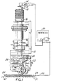
- the apparatus of the invention is incorporated into the head of a scribing machine 10 as described in US-A-4,641,773. Although a specific scribe machine head is shown, any device that can write wire would be acceptable.
- the wire 12 is fed from a supply source 14 and passed through a ferrite ring 15 to a conductive tube 16, which is electrically insulated from the rest of the scribing device. Ring 15 electrically isolates wire 12 from source 14.
- tube 16 is a brass tube.
- Wire 12 passes through brass tube 16 which is internally insulated.
- the combination of wire 12, internal insulation of brass tube 16, and surface conduction of brass tube 16 creates a capacitance in the system.
- the system comprises the entire assembly whose capacitance can be measured.
- Capacitance meter 20 can be of any make and of the range necessary for the purpose addressed below. In the depicted arrangement, the meter used is a Boonton 72B digital capacitance meter operating at a frequency of 1 MHz and at a voltage of 15 mV.
- Feeding mechanism is electrically isolated from the remaining portion of scribing head 10 by insulated blocks 24.
- wire 12 is affixed to a workpiece 26.
- a capacitance exists between the wire and the ground plane. This capacitance, or variations thereof, can be measured by a capacitance meter.
- Workpiece 26 rests on a panel with a metal panel 27 and is electrical connected therewith.
- Panel 27 is affixed to a shuttle plate 28.
- Shuttle plate 28 moves workpiece 26 and panel 27 and is electrically isolated from the scribing machine's supporting frame by an insulating layer 31.
- Shuttle plate 28 is connected to meter20 byelec- trical lead 32.
- lead 32 could also be connected to plane 27.
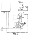
- Fig. 2 represents the major elements of this invention in further detail.
- Stylus 40 is generally shaped as shown in Fig. 2 including a magnetostrictive transducer42 coupled to a tapered horn 44.
- Transducer42 is made from a material having magnetostrictive properties, such as nickel, and is surrounded by a driving coil 46.
- the nodal point 48 at the center of transducer 42 is stationary, and the ends of the transducer vibrate in longitudinal direction.
- Insulated wire 12 is dispersed from a spool 14 and is supplied to the surface of the workpiece or a circuit board 26 via a wire feed drive system.
- the circuit board includes the substrate 50 coated with an adhesive coating 52 which is activatable by the application of ultrasonic energy generated by the vibration of stylus head 40. As the wire passes beneath rod 54 of ultrasonic stylus 40, ultrasonic energy is applied to activate the adhesive layer 52 on the circuit board 50 and to guide the wire in place in the adhesive.
- Agen- eral description of this scribing method is given in US-A 4,641,773.
- the two capacitors created are ground plane 56, insulator 50. and scribed wire 58, and feeding wire 12, and brass tube conductor 16.
- Fig. 2 shows A.C. source 60 which generates a 500 KHz fixed amplitude reference frequency.
- A.C. source 60 which generates a 500 KHz fixed amplitude reference frequency.
- a phase shift may be measured.
- the net capacitance of the system increases gradually as the length of the scribed wire 58 increases on the circuit board. In the event of a broken line the net capacitance drops drastically and the phase shift generated would be out of the expected range estimated for a wire that would not have been broken. This phase shift would be measured by the measuring means 62 (Fig. 2).
- Fig. 3 represents the system equivalent capacitors, C 1 70 and C 2 72 created by conductors and insulators as described in Fig. 2.
- A.C. source drive 62 generates a stable frequency with a constant amplitude signal. Amplitude regulation of the output signal of the A.C. drive 62 is accomplished by standard closed-loop feedback techni- i-ques. The sine wave generated preferably has very low harmonic frequency content.
- the output of drive 62 is connected to a synchronous detector 74 by conductor 76. This output serves as a reference voltage for further comparison between the signal driven through the system capacitance 78 and the original signal itself. Hence, the output of drive 62 is also connected to the system capacitor as depicted in Fig. 2 and represented in Fig. 4. Capacitor C x 78 represents the equivalent capacitance of the system.
- Conductor 80 connects the output of drive 62 to capacitor C x 78.
- the signal driven through capacitor C x 78 experiences a phase shift, the extent of which linearly depends on the value of the capacitor C x 78.
- This signal is then fed into current sensitive detector 82, basically consisting of a low impedance amplifier. Low impedance is accomplished by the implementation of a series resonant front end within the amplifier circuitry.
- the input current to the current sensitive detector 82 is a linear function of unknown capacitance, Therefore, the output signal 84 is also proportional to the capacitance.
- the output signal 84 of the current sensitive detector 82 is connected to the input of the synchronous detector 74.
- the other input of the synchronous detector 74 is directly connected to the output of the source drive 62.
- the synchronous detector function is to simultaneously compare with gain the coinciding wave forms provided by the A.C. source 60 and the current sensitive detector 82 thus extracting the reactive portion of the signal in a linear fashion.
- the synchronous detector 74 contains a precision wide band width analog multiplier 86. Assuming a pure sinusoidal frequency output from drive 62, the resultant signal of the multiplication by multiplier 86 will have two frequency components. One component is a D.C. signal, the amplitude of which is a function of the capacitor phase shift, and the other is a sine wave at almost double the source frequency. By feeding the resultant signal 88 from the multiplier 86 to a low pass filter 90 the high frequency component would be attenuated to zero and the resultant output of the synchronous detector 74 will be a D.C. output signal 92 whose magnitude is proportional to capacitance C x 78 of the system.
- C x would also vary. It is possible to estimate the range of the capacitance C x 78 under the system's normal condition without any unscheduled wire breakage. This, in turn, would indicate the approximate range of the D.C. signal output 92 of the synchronous detector 74. Any D.C. signal outside this estimated range would indicate a function failure and proper recourses could be taken upon such an indication. The system, however, experiences an inherent capacitive effect beyond the one defined in Fig. 3. This stray capacitance would limit the available measuring range of the D.C. signals.
- a method to eliminate the effect of stray capacitance in the system is represented in Fig. 5.
- Inductor 100 is connected in series with stray capacitors of the system prior to engagement of the wire on the board. By tuning inductor 100 it is possible to offset the capacitive phase shift resulting from the stray capacitance by an inductive phase shift in an opposite direction. Hence, by initiating the system, the effect of the stray capacitor would be totally eliminated.
- the rest of the circuit depicted in Fig. 5 is similar to the circuit of Fig. 4.
- the D.C. voltage 92 can be used to override the scribing power signal, cut off the feeder motor, and terminate the scribing process.
- Connectors 96 allow for connecting the measuring system to the scribing apparatus.
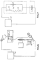
- Fig. 6 represents another embodiment of the present invention.
- the working spool 14 is wound so that the inside end of the wire 12 is exposed and one side of the broken wire monitor 62 can be directly connected to it.
- the other input of the broken wire monitor 62 is connected to either a shuttle plate 28 or a ground plate 27 in the panel (Fig. 1).
- Fig. 7 represents the electrical equivalent of the system using the wire termination method of Fig. 6.
- the inductance 110 and resistance 112 represent the winding on spool 14 (Fig. 6).
Landscapes
- Physics & Mathematics (AREA)
- General Physics & Mathematics (AREA)
- Testing Of Short-Circuits, Discontinuities, Leakage, Or Incorrect Line Connections (AREA)
- Investigating Or Analyzing Materials By The Use Of Electric Means (AREA)
- Measurement Of Resistance Or Impedance (AREA)
Applications Claiming Priority (2)
| Application Number | Priority Date | Filing Date | Title |
|---|---|---|---|
| US554130 | 1990-07-17 | ||
| US07/554,130 US5083087A (en) | 1990-07-17 | 1990-07-17 | Broken wire detector for wire scribing machines |
Publications (2)
| Publication Number | Publication Date |
|---|---|
| EP0477489A1 EP0477489A1 (en) | 1992-04-01 |
| EP0477489B1 true EP0477489B1 (en) | 1995-03-22 |
Family
ID=24212162
Family Applications (1)
| Application Number | Title | Priority Date | Filing Date |
|---|---|---|---|
| EP91111527A Expired - Lifetime EP0477489B1 (en) | 1990-07-17 | 1991-07-11 | Broken wire detector for wire scribing machines |
Country Status (8)
| Country | Link |
|---|---|
| US (1) | US5083087A (cs) |
| EP (1) | EP0477489B1 (cs) |
| JP (1) | JP3126414B2 (cs) |
| AU (1) | AU7433591A (cs) |
| CA (1) | CA2042071A1 (cs) |
| CS (1) | CS220291A3 (cs) |
| DE (1) | DE69108334T2 (cs) |
| HU (1) | HUT66406A (cs) |
Families Citing this family (15)
| Publication number | Priority date | Publication date | Assignee | Title |
|---|---|---|---|---|
| EP0594146B1 (en) * | 1992-10-22 | 2002-01-09 | Advanced Interconnection Technology, Inc. | System for automatic optical inspection of wire scribed circuit boards |
| US5556493A (en) * | 1995-01-13 | 1996-09-17 | Libbey-Owens-Ford Co. | Mounting an optical moisture sensor on a windshield using a vacuum chamber device |
| US5488308A (en) * | 1994-07-20 | 1996-01-30 | Kirka; Arde | Apparatus and method for detecting breakage of a drive band in a packaging machine |
| US6079607A (en) * | 1997-04-29 | 2000-06-27 | Texas Instruments Incorporated | Method for high frequency bonding |
| US6039234A (en) * | 1998-06-16 | 2000-03-21 | Kulicke & Soffa Investments, Inc. | Missing wire detector |
| US6667625B1 (en) * | 2001-12-31 | 2003-12-23 | Charles F. Miller | Method and apparatus for detecting wire in an ultrasonic bonding tool |
| US8322624B2 (en) * | 2007-04-10 | 2012-12-04 | Feinics Amatech Teoranta | Smart card with switchable matching antenna |
| US7581308B2 (en) | 2007-01-01 | 2009-09-01 | Advanced Microelectronic And Automation Technology Ltd. | Methods of connecting an antenna to a transponder chip |
| US7546671B2 (en) * | 2006-09-26 | 2009-06-16 | Micromechanic And Automation Technology Ltd. | Method of forming an inlay substrate having an antenna wire |
| US8608080B2 (en) * | 2006-09-26 | 2013-12-17 | Feinics Amatech Teoranta | Inlays for security documents |
| US8240022B2 (en) * | 2006-09-26 | 2012-08-14 | Feinics Amatech Teorowita | Methods of connecting an antenna to a transponder chip |
| US20080179404A1 (en) * | 2006-09-26 | 2008-07-31 | Advanced Microelectronic And Automation Technology Ltd. | Methods and apparatuses to produce inlays with transponders |
| US7979975B2 (en) * | 2007-04-10 | 2011-07-19 | Feinics Amatech Teavanta | Methods of connecting an antenna to a transponder chip |
| US7980477B2 (en) * | 2007-05-17 | 2011-07-19 | Féinics Amatech Teoranta | Dual interface inlays |
| US12196784B1 (en) * | 2022-01-18 | 2025-01-14 | National Technology & Engineering Solutions Of Sandia, Llc | Magnetostrictive current sensor method and system |
Family Cites Families (11)
| Publication number | Priority date | Publication date | Assignee | Title |
|---|---|---|---|---|
| US3674914A (en) * | 1968-02-09 | 1972-07-04 | Photocircuits Corp | Wire scribed circuit boards and method of manufacture |
| US3674602A (en) * | 1969-10-09 | 1972-07-04 | Photocircuits Corp | Apparatus for making wire scribed circuit boards |
| US3778707A (en) * | 1972-12-14 | 1973-12-11 | Agridustrial Electronics | Means for measuring loss tangent of material for determining moisture content |
| US3959723A (en) * | 1974-09-13 | 1976-05-25 | Wagner Delmer W | Lumber moisture measurement apparatus which is less sensitive to lumber movement and spacing |
| US3975680A (en) * | 1975-06-25 | 1976-08-17 | Honeywell Information Systems, Inc. | Non-contact coupling plate for circuit board tester |
| JPS57211240A (en) * | 1981-06-22 | 1982-12-25 | Hitachi Ltd | Wire bonder |
| US4565966A (en) * | 1983-03-07 | 1986-01-21 | Kollmorgen Technologies Corporation | Method and apparatus for testing of electrical interconnection networks |
| US4583042A (en) * | 1983-04-18 | 1986-04-15 | The Boeing Company | Capacitive circuit board testing system and method using a conductive pliant elastomeric reference plane |
| US4586642A (en) * | 1985-05-13 | 1986-05-06 | Kulicke And Soffa Industries Inc. | Wire bond monitoring system |
| US4693778A (en) * | 1985-07-19 | 1987-09-15 | Kollmorgen Technologies Corporation | Apparatus for making scribed circuit boards and circuit board modifications |
| US4641773A (en) * | 1985-08-09 | 1987-02-10 | Kollmorgen Technologies Corp. | Ultrasonic stylus position stabilizer |
-
1990
- 1990-07-17 US US07/554,130 patent/US5083087A/en not_active Expired - Fee Related
-
1991
- 1991-04-10 AU AU74335/91A patent/AU7433591A/en not_active Abandoned
- 1991-05-08 CA CA002042071A patent/CA2042071A1/en not_active Abandoned
- 1991-05-20 JP JP03145412A patent/JP3126414B2/ja not_active Expired - Fee Related
- 1991-07-11 DE DE69108334T patent/DE69108334T2/de not_active Expired - Fee Related
- 1991-07-11 EP EP91111527A patent/EP0477489B1/en not_active Expired - Lifetime
- 1991-07-16 CS CS912202A patent/CS220291A3/cs unknown
- 1991-07-17 HU HU912394A patent/HUT66406A/hu unknown
Also Published As
| Publication number | Publication date |
|---|---|
| DE69108334T2 (de) | 1996-03-21 |
| JPH05113461A (ja) | 1993-05-07 |
| US5083087A (en) | 1992-01-21 |
| JP3126414B2 (ja) | 2001-01-22 |
| AU7433591A (en) | 1992-01-23 |
| HUT66406A (en) | 1994-11-28 |
| CA2042071A1 (en) | 1992-01-18 |
| CS220291A3 (en) | 1992-03-18 |
| DE69108334D1 (de) | 1995-04-27 |
| HU912394D0 (en) | 1991-12-30 |
| EP0477489A1 (en) | 1992-04-01 |
Similar Documents
| Publication | Publication Date | Title |
|---|---|---|
| EP0477489B1 (en) | Broken wire detector for wire scribing machines | |
| JP2940815B2 (ja) | 導体回路基板の検査方法およびその検査装置 | |
| KR100908589B1 (ko) | 막두께 측정장치 | |
| US7096555B2 (en) | Closed loop backdrilling system | |
| CA1181933A (en) | Method and apparatus for ultrasonic bonding | |
| CA1217865A (en) | Determination of coating thickness | |
| JPH07111997B2 (ja) | 研磨作業における終点検出方法及び装置 | |
| CA2688905C (en) | Twisted-pair electrical cable testing | |
| US4825158A (en) | Method of detecting conductive material contained in glass fiber by detecting changes in amplitude and frequency of an oscillator and detecting apparatus therefor | |
| US3860866A (en) | Methods and apparatus for locating an open section in a conductor | |
| JP2589420B2 (ja) | 導電膜検査方法およびその装置 | |
| JP3793154B2 (ja) | 対向した表面間の距離を表す信号を生成するための無接触測定方法および装置 | |
| US4072895A (en) | Eddy current converter for non-destructive testing of electrically conducting coating in holes of printed circuit boards | |
| CN212540616U (zh) | 一种传感器装置 | |
| US20060292712A1 (en) | Process for the detection of a malfunction in a device for wire sawing and device for practicing said process | |
| Malikov et al. | Experimental Studies of Conductive Paths of Printed Circuit Boards by Using Subminiature Eddy Current Transducers | |
| JP2023151704A (ja) | 基板加工装置 | |
| KR100337524B1 (ko) | 미세회로 기판의 단선측정을 위한 비접촉 센서 | |
| CN116659367A (zh) | 一种pcb及其介质厚度检测方法 | |
| Town | A review of eccentricity, capacitance and diameter gauges for continuous observation and recording of cable quality during manufacture | |
| WO2000022375A1 (en) | Method and device for measuring cross-section of wires | |
| EP1056984A1 (en) | Apparatus for measuring properties of a moving paper web or cardboard web | |
| WO2008031925A1 (en) | Weld-wire-filler identification apparatus and method | |
| HU187108B (en) | Touchless tester, first of all for touchless testing surface of fibrous materials moving on it | |
| JPH04245111A (ja) | シールド電線のシールド欠陥検出方法 |
Legal Events
| Date | Code | Title | Description |
|---|---|---|---|
| PUAI | Public reference made under article 153(3) epc to a published international application that has entered the european phase |
Free format text: ORIGINAL CODE: 0009012 |
|
| AK | Designated contracting states |
Kind code of ref document: A1 Designated state(s): BE CH DE FR GB IT LI NL SE |
|
| 17P | Request for examination filed |
Effective date: 19920924 |
|
| 17Q | First examination report despatched |
Effective date: 19940111 |
|
| GRAA | (expected) grant |
Free format text: ORIGINAL CODE: 0009210 |
|
| AK | Designated contracting states |
Kind code of ref document: B1 Designated state(s): BE CH DE FR GB IT LI NL SE |
|
| ITF | It: translation for a ep patent filed | ||
| REF | Corresponds to: |
Ref document number: 69108334 Country of ref document: DE Date of ref document: 19950427 |
|
| PGFP | Annual fee paid to national office [announced via postgrant information from national office to epo] |
Ref country code: SE Payment date: 19950628 Year of fee payment: 5 |
|
| PGFP | Annual fee paid to national office [announced via postgrant information from national office to epo] |
Ref country code: GB Payment date: 19950710 Year of fee payment: 5 |
|
| PGFP | Annual fee paid to national office [announced via postgrant information from national office to epo] |
Ref country code: CH Payment date: 19950714 Year of fee payment: 5 |
|
| PGFP | Annual fee paid to national office [announced via postgrant information from national office to epo] |
Ref country code: FR Payment date: 19950720 Year of fee payment: 5 |
|
| ET | Fr: translation filed | ||
| PGFP | Annual fee paid to national office [announced via postgrant information from national office to epo] |
Ref country code: NL Payment date: 19950731 Year of fee payment: 5 |
|
| PGFP | Annual fee paid to national office [announced via postgrant information from national office to epo] |
Ref country code: BE Payment date: 19950809 Year of fee payment: 5 |
|
| PGFP | Annual fee paid to national office [announced via postgrant information from national office to epo] |
Ref country code: DE Payment date: 19950922 Year of fee payment: 5 |
|
| PLBE | No opposition filed within time limit |
Free format text: ORIGINAL CODE: 0009261 |
|
| STAA | Information on the status of an ep patent application or granted ep patent |
Free format text: STATUS: NO OPPOSITION FILED WITHIN TIME LIMIT |
|
| 26N | No opposition filed | ||
| PG25 | Lapsed in a contracting state [announced via postgrant information from national office to epo] |
Ref country code: GB Effective date: 19960711 |
|
| PG25 | Lapsed in a contracting state [announced via postgrant information from national office to epo] |
Ref country code: SE Effective date: 19960712 |
|
| PG25 | Lapsed in a contracting state [announced via postgrant information from national office to epo] |
Ref country code: LI Effective date: 19960731 Ref country code: CH Effective date: 19960731 Ref country code: BE Effective date: 19960731 |
|
| BERE | Be: lapsed |
Owner name: ADVANCED INTERCONNECTION TECHNOLOGY INC. Effective date: 19960731 |
|
| PG25 | Lapsed in a contracting state [announced via postgrant information from national office to epo] |
Ref country code: NL Effective date: 19970201 |
|
| GBPC | Gb: european patent ceased through non-payment of renewal fee |
Effective date: 19960711 |
|
| REG | Reference to a national code |
Ref country code: CH Ref legal event code: PL |
|
| PG25 | Lapsed in a contracting state [announced via postgrant information from national office to epo] |
Ref country code: FR Effective date: 19970328 |
|
| NLV4 | Nl: lapsed or anulled due to non-payment of the annual fee |
Effective date: 19970201 |
|
| PG25 | Lapsed in a contracting state [announced via postgrant information from national office to epo] |
Ref country code: DE Effective date: 19970402 |
|
| EUG | Se: european patent has lapsed |
Ref document number: 91111527.7 |
|
| REG | Reference to a national code |
Ref country code: FR Ref legal event code: ST |
|
| PG25 | Lapsed in a contracting state [announced via postgrant information from national office to epo] |
Ref country code: IT Free format text: LAPSE BECAUSE OF NON-PAYMENT OF DUE FEES Effective date: 20050711 |