EP0475766B1 - Fenster zum Durchlassen von Strahlung wie Mikrowellen - Google Patents
Fenster zum Durchlassen von Strahlung wie Mikrowellen Download PDFInfo
- Publication number
- EP0475766B1 EP0475766B1 EP91308349A EP91308349A EP0475766B1 EP 0475766 B1 EP0475766 B1 EP 0475766B1 EP 91308349 A EP91308349 A EP 91308349A EP 91308349 A EP91308349 A EP 91308349A EP 0475766 B1 EP0475766 B1 EP 0475766B1
- Authority
- EP
- European Patent Office
- Prior art keywords
- layer
- window according
- diamonds
- diamond
- resin
- Prior art date
- Legal status (The legal status is an assumption and is not a legal conclusion. Google has not performed a legal analysis and makes no representation as to the accuracy of the status listed.)
- Expired - Lifetime
Links
- 230000005855 radiation Effects 0.000 title claims abstract description 23
- 239000010432 diamond Substances 0.000 claims abstract description 51
- 229910003460 diamond Inorganic materials 0.000 claims abstract description 37
- 239000002952 polymeric resin Substances 0.000 claims abstract description 9
- 229920003002 synthetic resin Polymers 0.000 claims abstract description 9
- 229920005989 resin Polymers 0.000 claims description 26
- 239000011347 resin Substances 0.000 claims description 26
- 239000002245 particle Substances 0.000 claims description 9
- 229920001343 polytetrafluoroethylene Polymers 0.000 claims description 4
- 229920001187 thermosetting polymer Polymers 0.000 claims description 4
- KXGFMDJXCMQABM-UHFFFAOYSA-N 2-methoxy-6-methylphenol Chemical compound [CH]OC1=CC=CC([CH])=C1O KXGFMDJXCMQABM-UHFFFAOYSA-N 0.000 claims description 3
- 229920001568 phenolic resin Polymers 0.000 claims description 3
- 239000005011 phenolic resin Substances 0.000 claims description 3
- 239000003822 epoxy resin Substances 0.000 claims description 2
- LNEPOXFFQSENCJ-UHFFFAOYSA-N haloperidol Chemical compound C1CC(O)(C=2C=CC(Cl)=CC=2)CCN1CCCC(=O)C1=CC=C(F)C=C1 LNEPOXFFQSENCJ-UHFFFAOYSA-N 0.000 claims description 2
- 229920000647 polyepoxide Polymers 0.000 claims description 2
- 239000004810 polytetrafluoroethylene Substances 0.000 claims 1
- 239000010410 layer Substances 0.000 description 40
- 230000000694 effects Effects 0.000 description 2
- 235000013824 polyphenols Nutrition 0.000 description 2
- 239000006117 anti-reflective coating Substances 0.000 description 1
- 238000001816 cooling Methods 0.000 description 1
- 230000017525 heat dissipation Effects 0.000 description 1
- 150000002460 imidazoles Chemical class 0.000 description 1
- 150000003949 imides Chemical class 0.000 description 1
- 239000000463 material Substances 0.000 description 1
- 239000000155 melt Substances 0.000 description 1
- 238000002844 melting Methods 0.000 description 1
- 230000008018 melting Effects 0.000 description 1
- 239000000203 mixture Substances 0.000 description 1
- 150000003252 quinoxalines Chemical class 0.000 description 1
- 239000002356 single layer Substances 0.000 description 1
- 230000000930 thermomechanical effect Effects 0.000 description 1
Images
Classifications
-
- H—ELECTRICITY
- H01—ELECTRIC ELEMENTS
- H01P—WAVEGUIDES; RESONATORS, LINES, OR OTHER DEVICES OF THE WAVEGUIDE TYPE
- H01P1/00—Auxiliary devices
- H01P1/08—Dielectric windows
Definitions
- This invention relates to a window for transmitting radiation such as microwave radiation.
- the material which is used at present for making windows for transmitting microwave radiation is phenolic resin. While phenolic resin will transmit microwave radiation it has poor thermo-mechanical properties. To overcome this problem the window may be made in two layers which sandwich a cooling layer therebetween. Windows are difficult to make in this manner and, in any event, are not very efficient.
- United States Patent 3,895,313 describes a diamond window for transmitting a laser beam.
- a plurality of diamond polygons or window panes are held in a network of metallic tubes.
- a window for transmitting radiation of wavelength 20 microns or longer comprising a supported layer presenting a first major surface on one side capable of receiving the radiation, and a second major surface on the opposite side to the first major surface, the layer comprising a plurality of diamonds and a bonding polymeric resin capable of transmitting the radiation.
- the polymeric resin must be capable of transmitting the radiation.
- the presence of the diamond particles sharply increases the thermal conductivity of the resin layer by a factor of at least 3.
- One consequence of this is that the melt or working temperature of the resin layer is increased.
- Another consequence is that heat dissipation is improved.
- the window may thus be used in circumstances where higher temperatures are experienced and for radiation of greater energy than is possible with prior art resin layers.
- the resin/diamond layer will be a supported layer and will act, in effect, as a window pane in the support.
- the support will be provided around at least a part of the periphery of the layer, for example by means of a frame. Other supporting means known in the art may be used.
- the resin/diamond layer will have a thickness in the range 20 to 500 microns, preferably 20 to 250 microns. As a general rule, the thickness of the layer will be less than a quarter of the wavelength of the radiation passing through it.
- the polymeric resin will typically be selected from thermosetting resins, epoxy resins and PTFE (polytetrafluoroethene).
- suitable thermosetting resins are phenolics, e.g. phenolformaldehyhe, imides, quinoxalines and imidazoles.
- Specific examples of suitable resins are those sold under the trade names RUTAPHEN SP 309® and modified PHENOLIC AR1004®.
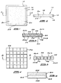
- a window for transmitting radiation of wavelenghs 20 microns or longer, i.e. microwave radiation comprises a layer 10 supported around its periphery 12 by a frame 14.
- the layer 10 presents major flat surfaces 16 and 18 on opposite sides thereof. In use, the one major surface will receive the microwave energy which will then pass through the layer and exit through the other major surface.
- the layer 10 comprises a plurality of discrete diamond particles 20 embedded in a polymeric resin 22.
- the diamond particles will generally be uniformly dispersed through the polymeric resin.
- the diamond particles will generally have a size in the range 20 to 200 microns.
- the concentration of the diamonds will vary according to the application to which the window is to be put. In general, the concentration of the diamonds in the layer will not exceed 65 percent by volume. A mixture of diamond particles of varying sizes may be used in the layer.
- Figure 3 illustrates another example of a resin/diamond layer.
- a plurality of diamond plates 24 are located in a polymeric resin 26.
- major flat surfaces 28 and 30 are provided on opposite sides thereof.
- the diamond plates 24 are positioned edge-on relative to their neighbours and form a monolayer of diamonds across the layer. If the resin in the regions 32 and 34 to either side of the upper and lower surfaces 24a and 24b of the diamond plates is thin, e.g. no more than 5 microns in thickness, then the window can be used for transmitting IR radiation as well as microwave radiation. Where these regions are thicker, then the layer is suitable for transmitting microwave radiation only.
- the resin/diamond layer comprises a plurality of diamond plates 40 each of which is located edge-on relative to its neighbours.
- the diamond plates 40 are bonded to each other by means of a bonding polymeric resin 42.
- the resin 42 thus provides a bonding network between the diamond plates.
- the top surface 40a and bottom surface 40b of each diamond plate 40 is not covered by resin.
- the layer as with the previous two embodiments, provides major flat surfaces 44 and 46 on opposite sides thereof.
- the layer of this embodiment may be used for transmitting IR or microwave radiation.
- the resin/diamond layer may comprise two or more sections of differing diamond concentration. Each layer will thus have a different dielectric constant with the one layer acting, in effect, as an anti-reflective coating for the other layer.
- An example of such a layer is illustrated by Figure 6. Referring to this figure, the layer comprises two sections 60 and 62 bonded to each other along the interface 64. This interface lies intermediate the major surfaces 66 and 68 of the layer. The diamond concentration of layer 60 is higher than that of the layer 62.
- the resin/diamond layers of the invention may be made in a mould by suitably locating resin and diamond particles in the mould which is heated, typically, to a temperature of 60°C. Thereafter, pressure is applied to the resin and diamond particles and the temperature raised until the melting point of the resin is reached. The pressure is released, the mould removed and the thus produced layer allowed to cool. If diamond plates are used, they will generally be positioned in the mould and the resin thereafter introduced into the mould. If diamond particles are used, they will generally be mixed with the resin prior to introduction into the mould.
Landscapes
- Glass Compositions (AREA)
- Electron Tubes For Measurement (AREA)
- Seal Device For Vehicle (AREA)
- Window Of Vehicle (AREA)
- Laminated Bodies (AREA)
- Waveguide Connection Structure (AREA)
- Special Wing (AREA)
- Constitution Of High-Frequency Heating (AREA)
Claims (14)
- Fenster zum Durchlassen von Strahlung einer Wellenlänge von 20 Mikrometer oder länger, mit einer gestützten Schicht (10), welche auf einer Seite eine erste Hauptfläche (16) aufweist, welche in der Lage ist, die Strahlung zu empfangen, und auf der der ersten Hauptfläche (16) abgewandten Seite eine zweite Hauptfläche (18) aufweist, wobei die Schicht (10) mehrere Diamanten (20) und ein Verbondungspolymerharz (22) aufweist, das in der Lage ist, die Strahlung durchzulassen.
- Fenster nach Anspruch 1, bei dem die Schicht (10) um wenigstens einen Teil ihres Umfangs (12) abgestützt ist.
- Fenster nach Anspruch 2, bei dem die Abstützung ein Rahmen (14) ist.
- Fenster nach einem der vorhergehenden Ansprüche, bei dem die Dicke der Schicht (10) im Bereich von 20 bis 500 Mikrometer liegt.
- Fenster nach einem der Ansprüche 1 bis 3, bei dem die Dicke der Schicht (10) im Bereich von 20 bis 250 Mikrometer liegt.
- Fenster nach einem der vorhergehenden Ansprüche, bei dem die Schicht (10) mehrere Diamanten (40) aufweist, die durch ein Netzwerk (42) des zwischen den Diamanten (40) angeordneten Harzes miteinander verbondet sind.
- Fenster nach Anspruch 6, bei dem die Diamanten (40) Diamantplatten sind, wobei jede Diamantplatte relativ zu benachbarten Diamantplatten in Kantenanlage positoniert ist.
- Fenster nach einem der Ansprüche 1 bis 5, bei dem die Schicht (10) mehrere in dem Harz (22) eingebettete Diamanten (20) aufweist.
- Fenster nach Anspruch 8, bei dem die Diamanten Diamantplatten (24) sind, wobei jede Diamantplatte (24) relativ zu benachbarten Diamantplatten (24) in Kantenanlage positioniert ist.
- Fenster nach Anspruch 8, bei dem die Diamanten Diamantpartikel (20) mit einer Größe im Bereich von 20 bis 200 Mikrometer sind.
- Fenster nach Anspruch 10, bei dem die Diamanten (20) in einer Menge von bis zu 65 Volumenprozent der Schicht in der Schicht (10) vorhanden sind.
- Fenster nach einem der vorhergehenden Ansprüche, bei dem das Harz (22) aus wärmehärtbaren Harzen, Epoxidharzen und PTFE 〈= Polytetrafluorethen〉 gewählt ist.
- Fenster nach Anspruch 12, bei dem das wärmehärtbare Harz (22) ein Phenolharz ist.
- Fenster nach einem der vorhergehenden Ansprüche, bei dem die Schicht (10) zwei oder mehr Abschnitte (60,62) aufweist, die an einer Grenzfläche (64) oder Grenzflächen, die zwischen den Hauptflächen (66,68) angeordnet sind, miteinander verbondet sind, wobei die Diamantenkonzentration der Abschnitte (60,62) unterschiedlich ist.
Applications Claiming Priority (2)
| Application Number | Priority Date | Filing Date | Title |
|---|---|---|---|
| GB909020096A GB9020096D0 (en) | 1990-09-14 | 1990-09-14 | Window |
| GB9020096 | 1990-09-14 |
Publications (3)
| Publication Number | Publication Date |
|---|---|
| EP0475766A2 EP0475766A2 (de) | 1992-03-18 |
| EP0475766A3 EP0475766A3 (en) | 1992-04-15 |
| EP0475766B1 true EP0475766B1 (de) | 1995-11-29 |
Family
ID=10682194
Family Applications (1)
| Application Number | Title | Priority Date | Filing Date |
|---|---|---|---|
| EP91308349A Expired - Lifetime EP0475766B1 (de) | 1990-09-14 | 1991-09-12 | Fenster zum Durchlassen von Strahlung wie Mikrowellen |
Country Status (7)
| Country | Link |
|---|---|
| US (1) | US5243311A (de) |
| EP (1) | EP0475766B1 (de) |
| JP (1) | JP3136179B2 (de) |
| AT (1) | ATE130960T1 (de) |
| DE (1) | DE69114969T2 (de) |
| GB (1) | GB9020096D0 (de) |
| ZA (1) | ZA917220B (de) |
Families Citing this family (4)
| Publication number | Priority date | Publication date | Assignee | Title |
|---|---|---|---|---|
| US5604635A (en) * | 1995-03-08 | 1997-02-18 | Brown University Research Foundation | Microlenses and other optical elements fabricated by laser heating of semiconductor doped and other absorbing glasses |
| US5768022A (en) * | 1995-03-08 | 1998-06-16 | Brown University Research Foundation | Laser diode having in-situ fabricated lens element |
| US6118358A (en) * | 1999-01-18 | 2000-09-12 | Crouch; David D. | High average-power microwave window with high thermal conductivity dielectric strips |
| GB201701173D0 (en) * | 2017-01-24 | 2017-03-08 | Element Six Tech Ltd | Synthetic diamond plates |
Family Cites Families (8)
| Publication number | Priority date | Publication date | Assignee | Title |
|---|---|---|---|---|
| CA578546A (en) * | 1959-06-30 | H. Colbert William | Electrically conductive articles | |
| US2932806A (en) * | 1958-12-02 | 1960-04-12 | Bomac Lab Inc | Broadband microwave window |
| US3095550A (en) * | 1959-04-09 | 1963-06-25 | Timothy J Kilduff | Polytetrafluoroethylene waveguide window construction |
| US3895313A (en) * | 1973-09-17 | 1975-07-15 | Entropy Conversion | Laser systems with diamond optical elements |
| US4688009A (en) * | 1985-05-13 | 1987-08-18 | Varian Associates, Inc. | Triple-pane waveguide window |
| US4719436A (en) * | 1986-08-04 | 1988-01-12 | The United States Of America As Represented By The United States Department Of Energy | Stabilized chromium oxide film |
| JPS63149901A (ja) * | 1986-12-15 | 1988-06-22 | Toshiba Corp | マイクロ波装置 |
| ZA896979B (en) * | 1988-09-14 | 1990-06-27 | De Beers Ind Diamond | Diamond-containing product |
-
1990
- 1990-09-14 GB GB909020096A patent/GB9020096D0/en active Pending
-
1991
- 1991-09-11 ZA ZA917220A patent/ZA917220B/xx unknown
- 1991-09-12 DE DE69114969T patent/DE69114969T2/de not_active Expired - Fee Related
- 1991-09-12 EP EP91308349A patent/EP0475766B1/de not_active Expired - Lifetime
- 1991-09-12 AT AT91308349T patent/ATE130960T1/de not_active IP Right Cessation
- 1991-09-13 JP JP03310291A patent/JP3136179B2/ja not_active Expired - Fee Related
- 1991-09-16 US US07/760,104 patent/US5243311A/en not_active Expired - Fee Related
Also Published As
| Publication number | Publication date |
|---|---|
| EP0475766A3 (en) | 1992-04-15 |
| GB9020096D0 (en) | 1990-10-24 |
| JP3136179B2 (ja) | 2001-02-19 |
| ATE130960T1 (de) | 1995-12-15 |
| US5243311A (en) | 1993-09-07 |
| DE69114969D1 (de) | 1996-01-11 |
| DE69114969T2 (de) | 1996-05-15 |
| ZA917220B (en) | 1992-05-27 |
| EP0475766A2 (de) | 1992-03-18 |
| JPH05191101A (ja) | 1993-07-30 |
Similar Documents
| Publication | Publication Date | Title |
|---|---|---|
| US4278875A (en) | Electrically heated window | |
| EP0707950B1 (de) | Verfahren und Vorrichtung zur Verbindung von Glasscheiben | |
| US6919504B2 (en) | Flexible heat sink | |
| US5228947A (en) | Microwave curing system | |
| US4496415A (en) | Method for impregnating resin powder directly into a laminate lay up | |
| US20020176158A1 (en) | Infrared transparent optical element and infrared imaging camera using the same | |
| EP0218191A2 (de) | Herstellung von Mehrschichtstrukturen durch dielektrische Heizung eines Klebefilms | |
| US5858496A (en) | Optically transparent article with embedded mesh | |
| EP0475766B1 (de) | Fenster zum Durchlassen von Strahlung wie Mikrowellen | |
| KR101989077B1 (ko) | 열제어능을 구비한 방열부재, 방열시트 및 이의 제조방법 | |
| KR100447820B1 (ko) | 수지/구리/금속 적층물 및 이의 제조 방법 | |
| US20090100872A1 (en) | Method for laminating glass, glass-ceramic, or ceramic layers | |
| US5329569A (en) | X-ray transmissive debris shield | |
| EP0274789A2 (de) | Verfahren zum Herstellen eines geschichteten Aufbaus, sowie nach dem Verfahren hergestellter Schichtverbund | |
| JPS58139405A (ja) | 抵抗素子の製造方法 | |
| AU653488B2 (en) | Microwave heating system | |
| WO1998008640A2 (en) | Structure comprising honeycomb core and outer skin and method for its fabrication | |
| KR101807792B1 (ko) | 다수의 선형배열 광원들과 적어도 하나의 실린더리컬 렌즈 및 투광부를 구비한 직사각형 마스크를 이용한 이방전도성 필름 선형배열 레이저빔 접합장치 | |
| DE3586509T2 (de) | Verfahren zum laminieren eines films auf ein gewebe. | |
| JP2000059084A (ja) | 透明電磁波シールド板の製造方法 | |
| US20050105018A1 (en) | Light polarizing film, a method of continuously fabricating same, and reflective optical devices using same | |
| JPH06263899A (ja) | 導電性樹脂シートとその製造方法 | |
| KR102591403B1 (ko) | 복합 방열 하이브리드 시트 | |
| JP3443137B2 (ja) | ポリカーボネート樹脂積層板の製造方法 | |
| US5368674A (en) | Method of treating glass fiber-based prepreg |
Legal Events
| Date | Code | Title | Description |
|---|---|---|---|
| PUAI | Public reference made under article 153(3) epc to a published international application that has entered the european phase |
Free format text: ORIGINAL CODE: 0009012 |
|
| PUAL | Search report despatched |
Free format text: ORIGINAL CODE: 0009013 |
|
| AK | Designated contracting states |
Kind code of ref document: A2 Designated state(s): AT BE CH DE FR GB LI NL SE |
|
| AK | Designated contracting states |
Kind code of ref document: A3 Designated state(s): AT BE CH DE FR GB LI NL SE |
|
| 17P | Request for examination filed |
Effective date: 19920414 |
|
| 17Q | First examination report despatched |
Effective date: 19941021 |
|
| GRAA | (expected) grant |
Free format text: ORIGINAL CODE: 0009210 |
|
| AK | Designated contracting states |
Kind code of ref document: B1 Designated state(s): AT BE CH DE FR GB LI NL SE |
|
| PG25 | Lapsed in a contracting state [announced via postgrant information from national office to epo] |
Ref country code: AT Effective date: 19951129 |
|
| REF | Corresponds to: |
Ref document number: 130960 Country of ref document: AT Date of ref document: 19951215 Kind code of ref document: T |
|
| REF | Corresponds to: |
Ref document number: 69114969 Country of ref document: DE Date of ref document: 19960111 |
|
| REG | Reference to a national code |
Ref country code: CH Ref legal event code: NV Representative=s name: BOVARD AG PATENTANWAELTE |
|
| ET | Fr: translation filed | ||
| PGFP | Annual fee paid to national office [announced via postgrant information from national office to epo] |
Ref country code: CH Payment date: 19960919 Year of fee payment: 6 |
|
| PLBE | No opposition filed within time limit |
Free format text: ORIGINAL CODE: 0009261 |
|
| STAA | Information on the status of an ep patent application or granted ep patent |
Free format text: STATUS: NO OPPOSITION FILED WITHIN TIME LIMIT |
|
| 26N | No opposition filed | ||
| PG25 | Lapsed in a contracting state [announced via postgrant information from national office to epo] |
Ref country code: LI Free format text: LAPSE BECAUSE OF NON-PAYMENT OF DUE FEES Effective date: 19970930 Ref country code: CH Free format text: LAPSE BECAUSE OF NON-PAYMENT OF DUE FEES Effective date: 19970930 |
|
| PGFP | Annual fee paid to national office [announced via postgrant information from national office to epo] |
Ref country code: BE Payment date: 19971104 Year of fee payment: 7 |
|
| REG | Reference to a national code |
Ref country code: CH Ref legal event code: PL |
|
| PG25 | Lapsed in a contracting state [announced via postgrant information from national office to epo] |
Ref country code: BE Free format text: LAPSE BECAUSE OF NON-PAYMENT OF DUE FEES Effective date: 19980930 |
|
| BERE | Be: lapsed |
Owner name: DE BEERS INDUSTRIAL DIAMOND DIVISION (PROPRIETARY Effective date: 19980930 |
|
| PGFP | Annual fee paid to national office [announced via postgrant information from national office to epo] |
Ref country code: SE Payment date: 20010906 Year of fee payment: 11 |
|
| PGFP | Annual fee paid to national office [announced via postgrant information from national office to epo] |
Ref country code: FR Payment date: 20010911 Year of fee payment: 11 |
|
| PGFP | Annual fee paid to national office [announced via postgrant information from national office to epo] |
Ref country code: GB Payment date: 20010912 Year of fee payment: 11 |
|
| PGFP | Annual fee paid to national office [announced via postgrant information from national office to epo] |
Ref country code: DE Payment date: 20010924 Year of fee payment: 11 |
|
| PGFP | Annual fee paid to national office [announced via postgrant information from national office to epo] |
Ref country code: NL Payment date: 20010927 Year of fee payment: 11 |
|
| REG | Reference to a national code |
Ref country code: GB Ref legal event code: IF02 |
|
| PG25 | Lapsed in a contracting state [announced via postgrant information from national office to epo] |
Ref country code: GB Free format text: LAPSE BECAUSE OF NON-PAYMENT OF DUE FEES Effective date: 20020912 |
|
| PG25 | Lapsed in a contracting state [announced via postgrant information from national office to epo] |
Ref country code: SE Free format text: LAPSE BECAUSE OF NON-PAYMENT OF DUE FEES Effective date: 20020913 |
|
| PG25 | Lapsed in a contracting state [announced via postgrant information from national office to epo] |
Ref country code: NL Free format text: LAPSE BECAUSE OF NON-PAYMENT OF DUE FEES Effective date: 20030401 Ref country code: DE Free format text: LAPSE BECAUSE OF NON-PAYMENT OF DUE FEES Effective date: 20030401 |
|
| GBPC | Gb: european patent ceased through non-payment of renewal fee |
Effective date: 20020912 |
|
| EUG | Se: european patent has lapsed | ||
| PG25 | Lapsed in a contracting state [announced via postgrant information from national office to epo] |
Ref country code: FR Free format text: LAPSE BECAUSE OF NON-PAYMENT OF DUE FEES Effective date: 20030603 |
|
| REG | Reference to a national code |
Ref country code: FR Ref legal event code: ST |