EP0473370B1 - Gain control circuit - Google Patents
Gain control circuit Download PDFInfo
- Publication number
- EP0473370B1 EP0473370B1 EP91307759A EP91307759A EP0473370B1 EP 0473370 B1 EP0473370 B1 EP 0473370B1 EP 91307759 A EP91307759 A EP 91307759A EP 91307759 A EP91307759 A EP 91307759A EP 0473370 B1 EP0473370 B1 EP 0473370B1
- Authority
- EP
- European Patent Office
- Prior art keywords
- gain
- signal
- supplied
- vca
- circuit
- Prior art date
- Legal status (The legal status is an assumption and is not a legal conclusion. Google has not performed a legal analysis and makes no representation as to the accuracy of the status listed.)
- Expired - Lifetime
Links
Images
Classifications
-
- H—ELECTRICITY
- H03—ELECTRONIC CIRCUITRY
- H03G—CONTROL OF AMPLIFICATION
- H03G3/00—Gain control in amplifiers or frequency changers
- H03G3/20—Automatic control
-
- H—ELECTRICITY
- H03—ELECTRONIC CIRCUITRY
- H03F—AMPLIFIERS
- H03F3/00—Amplifiers with only discharge tubes or only semiconductor devices as amplifying elements
- H03F3/72—Gated amplifiers, i.e. amplifiers which are rendered operative or inoperative by means of a control signal
-
- H—ELECTRICITY
- H03—ELECTRONIC CIRCUITRY
- H03G—CONTROL OF AMPLIFICATION
- H03G1/00—Details of arrangements for controlling amplification
- H03G1/04—Modifications of control circuit to reduce distortion caused by control
-
- H—ELECTRICITY
- H03—ELECTRONIC CIRCUITRY
- H03G—CONTROL OF AMPLIFICATION
- H03G3/00—Gain control in amplifiers or frequency changers
-
- H—ELECTRICITY
- H03—ELECTRONIC CIRCUITRY
- H03G—CONTROL OF AMPLIFICATION
- H03G3/00—Gain control in amplifiers or frequency changers
- H03G3/20—Automatic control
- H03G3/30—Automatic control in amplifiers having semiconductor devices
- H03G3/3005—Automatic control in amplifiers having semiconductor devices in amplifiers suitable for low-frequencies, e.g. audio amplifiers
-
- H—ELECTRICITY
- H03—ELECTRONIC CIRCUITRY
- H03K—PULSE TECHNIQUE
- H03K17/00—Electronic switching or gating, i.e. not by contact-making and –breaking
- H03K17/51—Electronic switching or gating, i.e. not by contact-making and –breaking characterised by the components used
- H03K17/56—Electronic switching or gating, i.e. not by contact-making and –breaking characterised by the components used by the use, as active elements, of semiconductor devices
- H03K17/60—Electronic switching or gating, i.e. not by contact-making and –breaking characterised by the components used by the use, as active elements, of semiconductor devices the devices being bipolar transistors
- H03K17/66—Switching arrangements for passing the current in either direction at will; Switching arrangements for reversing the current at will
- H03K17/665—Switching arrangements for passing the current in either direction at will; Switching arrangements for reversing the current at will connected to one load terminal only
- H03K17/666—Switching arrangements for passing the current in either direction at will; Switching arrangements for reversing the current at will connected to one load terminal only the output circuit comprising more than one controlled bipolar transistor
- H03K17/667—Switching arrangements for passing the current in either direction at will; Switching arrangements for reversing the current at will connected to one load terminal only the output circuit comprising more than one controlled bipolar transistor using complementary bipolar transistors
Definitions
- the present invention relates to a servo circuit and, more particularly, to a means for controlling a variable gain amplifier to process an audio signal in a television receiver, a stereo apparatus or the like.
- a servo circuit for controlling the gain in a signal, which is to be processed, by changing a control voltage or current supplied to a variable gain amplifier (hereinafter referred to as VCA) to vary the gain of such amplifier.
- VCA variable gain amplifier
- Servo circuits are classified into a closed loop type and an open loop type, and a variety of methods and circuit configurations are presently contrived for controlling a VCA.
- IC integrated circuit
- a temperature characteristic canceller is inserted in a VCA control path to improve the temperature characteristic of an entire servo circuit, or a switch means is inserted for halting the VCA gain variation in a certain state so as not to cause any gain change in the VCA despite any level change of the control signal.
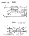
- Fig. 1 is an exemplary block diagram of a conventional closed-loop servo circuit.
- a process signal S1 fed to a process signal input terminal T1 is supplied to a VCA 1
- a control signal S2 fed to a control signal input terminal T2 is supplied to a first level detector 2.
- a VCA output signal S3 is delivered to an output terminal T3 and then is supplied to a second level detector 3.
- Output signals S4 and S5 of such first and second level detectors 2, 3 are added to each other by an adder 5 with the polarities thereof rendered mutually inverse.
- An output S6 of the adder 5 is delivered to a controller 4, which produces a control signal S7 for controlling the gain of the VCA 1 in accordance with the polarity of the input signal and then delivers the signal S7 to a limiter 6.
- a control signal S7 for increasing the gain of the VCA 1 is outputted from the controller 4 in case the adder output S6 is positive, whereby the gain of the VCA 1 is increased so that, in the two signals supplied to the adder 5, the negative signal S5 is gradually rendered greater, and the servo action is completed upon arrival of the adder output at zero.
- the limiter 6 is supplied with an upper limit setting signal S8 from an upper limit generator 7 and also with a lower limit setting signal S9 from a lower limit generator 8, and serves to change its output signal S10 between the upper and lower limit values.
- the output signal S10 from the limiter 6 is supplied to a temperature characteristic canceller 9 provided for cancelling the temperature characteristic included in the control characteristics of the VCA 1.
- the signal S10 obtained from the limiter 6 is outputted as a gain control signal S11 from the temperature characteristic canceller 9 and then is delivered to the VCA 1.
- Fig. 1 representing an exemplary case where the servo circuit is formed into a closed loop
- Fig. 2 a similar operation is performed also in another case of Fig. 2 where the servo circuit is formed into an open loop.
- a constant voltage circuit (or constant current circuit) is required to cancel the temperature characteristic of the upper limit setting signal 58 and the lower limit setting signal S9.
- the provision of such cancel circuit renders the entire servo circuit configuration further complicated.
- the circuit configuration may be simplified by the use of a limiter 6 with a diode, zener diode or similar element, any limiter with such element has a temperature characteristic and therefore some disadvantages are induced inclusive of non-uniform operation and characteristic variations due to temperature fluctuations.
- a servo circuit comprising:
- the upper and lower limits of the gain variable range in the amplitude limiter are changed in inverse fashion with temperature to the change in the gain in the variable gain amplifier, thereby cancelling the temperature variation overall with a simplified circuit configuration.
- the limiter may be used in a closed-loop or openloop servo circuit.
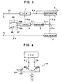
- Figure 3 is a block diagram of a closed-loop servo circuit according to a first embodiment of the present invention.
- the first embodiment is approximately similar to the aforementioned conventional servo circuit of Figure 1 with regard to the circuit configuration as a whole. More specifically, a process signal S1 fed to a process signal input terminal T1 is supplied to a VCA 1, and a control signal S2 fed to a control signal input terminal T2 is supplied to a first level detector 2. In the meantime, the VCA output S3 is delivered to an output terminal T3 while being supplied to a second level detector 3. And respective output signals S4 and S5 of the first and second level detectors 2, 3 are added to each other by an adder 5 in such a manner that the polarities thereof are rendered mutually inverse. Thereafter an output S6 of the adder 5 is delivered to a controller 4.
- the controller 4 produces a control signal S7 for controlling the gain of the VCA 1 in accordance with the polarity of the input signal and then delivers the signal S7 to a limiter 6.
- a control signal S7 for increasing the gain of the VCA 1 is outputted from the controller 4 in case the adder output S6 is positive, whereby the gain of the VCA 1 is increased so that, in the two signals supplied to the adder 5, the negative signal is gradually rendered greater, and the servo action is completed upon arrival of the adder outputs S6 at zero.
- the limiter 6 is supplied with an upper limit setting signal S38 from an upper limit generator 48 in a gain control range determiner 47 and also with a lower limit setting signal S39 from a lower limit generator 48, and serves to change its output signal S40, which corresponds to the gain control signal S11 in Figure 1, between such upper and lower limit values.
- the output signal S40 from the limiter 6 is supplied as a gain control signal to the VCA 1, which then performs an operation of varying the gain within the range determined by the gain control range determiner 47.
- the gain control in the VCA 1 is generally executed by, as shown in Figure 4, changing the ratio of the output currents, which flow in transistors Q2 and Q3 of a differential amplifier 51 respectively, by means of a control voltage adjuster 52 to thereby change the operating state of the circuit.
- the ratio of the output currents I1 and I2 of the transistors Q2 and Q3 is expressed as follows in relation to the control voltage Vc of the control voltage adjuster 52.
- I 1 /I 2 exp (q Vc/kT)
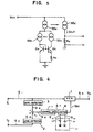
- Figure 5 represents an exemplary current mirror circuit comprising first to fourth constant current sources 55a, 55b, 55c, 55d; first and second transistors Q4, Q5; a resistor R2 connected between the emitter of the transistor Q5 and the ground; and a resistor R3 connected between the constant current source 55d and the ground.
- the output voltage of much current mirror circuit is obtained across the resistor R3.
- the output current I out flowing in the resistor R3 is expressed as follows in relation to the ratio 1 : n between the emitter area of the transistor Q4 and that of the transistor Q5.
- I out ⁇ (2kT/q) ⁇ l n ⁇ n ⁇ /R2
- V LIMIT (R3/R2) ⁇ (2kT/q) l n ⁇ n
- the output voltage V LIMIT is in direct proportion to the absolute temperature T. Consequently, under the conditions that the circuit of Figure 5 is used for both the upper limit generator 48 and the lower limit generator 49 in Figure 3, if the voltages V LIMIT outputted from such limit generators are utilised as upper and lower limit values of the control voltage for the VCA 1, then the temperature characteristics in the gain control range of the entire servo circuit cancel each other to become zero. Accordingly, an improved servo circuit free from a temperature characteristic in the gain control range can be accomplished by the present invention with a simplified circuit configuration.
- the output signal of the VCA 1 Is inputted directly to the level detector 3.
- the circuit configuration may be so modified as to execute some signal process before supplying the VCA output signal to the level detector 3.
- the characteristics of the controller 4 and the level detectors 2, 3 can be set freely to desired ones.
- the servo circuit of the present invention is properly applicable also to an open-loop type as shown in a circuit block diagram of Figure 6.
- each of the upper limit setting signal S48 and the lower limit setting signal S49 is supplied in the form of a voltage to the limiter 6, such signals S48 and S49 may be provided in the form of a current as well. In the latter case, where the current signals are supplied, the output current I OUT in Figure 5 may be directly taken out and fed to the limiter 6.
- the existing means for generating a voltage (current) directly proportional to the temperature as shown in Figure 5 is utilizable since it is generally incorporated in an IC, and therefore the servo circuit can be constituted free from a temperature characteristic without causing any substantial enlargement of the circuit scale.
- the present invention is so contrived that the temperature coefficient of the VCA and that of the amplitude limiter for setting upper and lower limits of the gain variable range in the VCA are rendered mutually inverse in polarity, so that if the characteristic of the VCA and the temperature characteristic within the gain variable range preset by the amplitude limiter are changed due to temperature fluctuations, such changes cancel each other to consequently reduce to zero the temperature characteristic in the gain control range of the entire servo circuit.
- the present invention is so contrived that the temperature coefficient of the VCA and that of the amplitude limiter for setting upper and lower limits of the gain variable range in the VCA are rendered mutually inverse in polarity, so that if the characteristic of the VCA and the temperature characteristic within the gain variable range preset by the amplitude limiter are changed due to temperature fluctuations, such changes cancel each other to consequently reduce to zero the temperature characteristic in the gain control range of the entire servo circuit.
Landscapes
- Engineering & Computer Science (AREA)
- Multimedia (AREA)
- Power Engineering (AREA)
- Optical Recording Or Reproduction (AREA)
- Control Of Amplification And Gain Control (AREA)
- Amplifiers (AREA)
- Tone Control, Compression And Expansion, Limiting Amplitude (AREA)
- Feedback Control In General (AREA)
Description
- The present invention relates to a servo circuit and, more particularly, to a means for controlling a variable gain amplifier to process an audio signal in a television receiver, a stereo apparatus or the like.
- There is known a servo circuit for controlling the gain in a signal, which is to be processed, by changing a control voltage or current supplied to a variable gain amplifier (hereinafter referred to as VCA) to vary the gain of such amplifier. Servo circuits are classified into a closed loop type and an open loop type, and a variety of methods and circuit configurations are presently contrived for controlling a VCA. However, in forming such servo circuit into an IC (integrated circuit) configuration, there exist some disadvantages relative to characteristic non-uniformity derived from temperature characteristic or with regard to the specific characteristic inherent in a bipolar-transistor IC. According to the known methods, a temperature characteristic canceller is inserted in a VCA control path to improve the temperature characteristic of an entire servo circuit, or a switch means is inserted for halting the VCA gain variation in a certain state so as not to cause any gain change in the VCA despite any level change of the control signal.
- In the conventional servo circuit, if the VCA control characteristics or the upper and lower limits of the control voltage or current have a temperature characteristic, it follows that the gain control range of the servo circuit as a whole comes to have a temperature characteristic.
- Fig. 1 is an exemplary block diagram of a conventional closed-loop servo circuit. In this diagram, a process signal S1 fed to a process signal input terminal T1 is supplied to a VCA 1, and a control signal S2 fed to a control signal input terminal T2 is supplied to a
first level detector 2. Meanwhile a VCA output signal S3 is delivered to an output terminal T3 and then is supplied to asecond level detector 3. Output signals S4 and S5 of such first andsecond level detectors adder 5 with the polarities thereof rendered mutually inverse. An output S6 of theadder 5 is delivered to acontroller 4, which produces a control signal S7 for controlling the gain of the VCA 1 in accordance with the polarity of the input signal and then delivers the signal S7 to alimiter 6. For example, when the level detection outputs S4 and S5 of the polarities shown are supplied to theadder 5, a control signal S7 for increasing the gain of the VCA 1 is outputted from thecontroller 4 in case the adder output S6 is positive, whereby the gain of the VCA 1 is increased so that, in the two signals supplied to theadder 5, the negative signal S5 is gradually rendered greater, and the servo action is completed upon arrival of the adder output at zero. - The
limiter 6 is supplied with an upper limit setting signal S8 from anupper limit generator 7 and also with a lower limit setting signal S9 from alower limit generator 8, and serves to change its output signal S10 between the upper and lower limit values. - The output signal S10 from the
limiter 6 is supplied to a temperature characteristic canceller 9 provided for cancelling the temperature characteristic included in the control characteristics of the VCA 1. The signal S10 obtained from thelimiter 6 is outputted as a gain control signal S11 from the temperature characteristic canceller 9 and then is delivered to the VCA 1. - In addition to Fig. 1 representing an exemplary case where the servo circuit is formed into a closed loop, a similar operation is performed also in another case of Fig. 2 where the servo circuit is formed into an open loop.
- In the conventional servo circuit of the configuration mentioned, it is necessary to insert a canceller 9 for cancelling the temperature characteristic included in the control characteristics of the VCA 1 as described, hence enlarging the circuit scale while increasing the power consumption and the production cost as well.
- Since it is not desired that the signals S8 and S9 outputted respectively from the
upper limit generator 7 and thelower limit generator 8 have a temperature characteristic, a constant voltage circuit (or constant current circuit) is required to cancel the temperature characteristic of the upper limit setting signal 58 and the lower limit setting signal S9. However, the provision of such cancel circuit renders the entire servo circuit configuration further complicated. Although the circuit configuration may be simplified by the use of alimiter 6 with a diode, zener diode or similar element, any limiter with such element has a temperature characteristic and therefore some disadvantages are induced inclusive of non-uniform operation and characteristic variations due to temperature fluctuations. - According to the present invention, there is provided a servo circuit comprising:
- a variable gain amplifier having a variable gain range and a gain that is variable in response to a gain control signal and in inverse proportion to the absolute temperature;
- an amplitude limiter for setting an upper limit and a lower limit of the variable gain range of said variable gain amplifier;
- a gain control range setting means for setting the upper and lower limits of the gain range in said amplitude limiter; characterised in that said gain control range setting means is adapted to change the upper and lower limits of the gain range in direct proportion to the absolute temperature.
- Thus, the upper and lower limits of the gain variable range in the amplitude limiter are changed in inverse fashion with temperature to the change in the gain in the variable gain amplifier, thereby cancelling the temperature variation overall with a simplified circuit configuration.
- The limiter may be used in a closed-loop or openloop servo circuit.
- The invention will be further described by way of non-limitative example, with reference to the accompanying drawings, in which:-
- Figure 1 is a block diagram of a conventional closed-loop servo circuit with a temperature
characteristic canceller employed in a feedback circuit; - Figure 2 is a block diagram of a conventional open-loop servo circuit with a temperature characteristic canceller;
- Figure 3 is a block diagram of a first embodiment of the present invention representing a closed-loop servo circuit with a limiter employed for control of a VCA;
- Figure 4 is a circuit diagram of a differential amplifier for explaining the gain control method executed in the first embodiment of the present invention shown in Figure 3;
- Figure 5 is a circuit diagram of a means for generating a voltage to determine the control range shown in the first embodiment of Figure 3; and
- Figure 6 is a block diagram of a second embodiment of the present invention representing an open-loop servo circuit with a limiter.
- Hereinafter, some preferred embodiments of the present invention will be described in detail with reference to the accompanying drawings.
- Figure 3 is a block diagram of a closed-loop servo circuit according to a first embodiment of the present invention.
- As obvious from this diagram, the first embodiment is approximately similar to the aforementioned conventional servo circuit of Figure 1 with regard to the circuit configuration as a whole. More specifically, a process signal S1 fed to a process signal input terminal T1 is supplied to a VCA 1, and a control signal S2 fed to a control signal input terminal T2 is supplied to a
first level detector 2. In the meantime, the VCA output S3 is delivered to an output terminal T3 while being supplied to asecond level detector 3. And respective output signals S4 and S5 of the first andsecond level detectors adder 5 in such a manner that the polarities thereof are rendered mutually inverse. Thereafter an output S6 of theadder 5 is delivered to acontroller 4. - The
controller 4 produces a control signal S7 for controlling the gain of the VCA 1 in accordance with the polarity of the input signal and then delivers the signal S7 to alimiter 6. For example, when the level detection outputs S4 and S5 of the polarities shown are supplied to theadder 5, a control signal S7 for increasing the gain of the VCA 1 is outputted from thecontroller 4 in case the adder output S6 is positive, whereby the gain of the VCA 1 is increased so that, in the two signals supplied to theadder 5, the negative signal is gradually rendered greater, and the servo action is completed upon arrival of the adder outputs S6 at zero. - The
limiter 6 is supplied with an upper limit setting signal S38 from anupper limit generator 48 in a gaincontrol range determiner 47 and also with a lower limit setting signal S39 from alower limit generator 48, and serves to change its output signal S40, which corresponds to the gain control signal S11 in Figure 1, between such upper and lower limit values. - The output signal S40 from the
limiter 6 is supplied as a gain control signal to the VCA 1, which then performs an operation of varying the gain within the range determined by the gaincontrol range determiner 47. - The gain control in the VCA 1 is generally executed by, as shown in Figure 4, changing the ratio of the output currents, which flow in transistors Q2 and Q3 of a
differential amplifier 51 respectively, by means of acontrol voltage adjuster 52 to thereby change the operating state of the circuit. - In the circuit for controlling the gain in the manner described, the ratio of the output currents I₁ and I₂ of the transistors Q2 and Q3 is expressed as follows in relation to the control voltage Vc of the
control voltage adjuster 52.
- Generally, the circuit is so formed as to keep the gain of the VCA 40 proportional to the ratio I₁/I₂. Therefore, in relation to a proportion constant α, the gain A of the VCA 1 is expressed as

- Accordingly, it is found that the logarithmic gain of the VCA shown in Figure 4 is inversely proportional to the absolute temperature T.
- Meanwhile, the means for generating a voltage directly proportional to the absolute temperature T may be such as shown in a circuit diagram of Figure 5 which is considered adequate to realise an IC configuration. Figure 5 represents an exemplary current mirror circuit comprising first to fourth constant
current sources current source 55d and the ground. The output voltage of much current mirror circuit is obtained across the resistor R3. - In the circuit of Figure 5, the output current Iout flowing in the resistor R3 is expressed as follows in relation to the ratio 1 : n between the emitter area of the transistor Q4 and that of the transistor Q5.

- Therefore the upper or lower limit VLIMIT of the control voltage obtained from the resistor R3 is given by

- Thus, the output voltage VLIMIT is in direct proportion to the absolute temperature T. Consequently, under the conditions that the circuit of Figure 5 is used for both the
upper limit generator 48 and thelower limit generator 49 in Figure 3, if the voltages VLIMIT outputted from such limit generators are utilised as upper and lower limit values of the control voltage for the VCA 1, then the temperature characteristics in the gain control range of the entire servo circuit cancel each other to become zero. Accordingly, an improved servo circuit free from a temperature characteristic in the gain control range can be accomplished by the present invention with a simplified circuit configuration. In the exemplary circuit of Figure 3, the output signal of the VCA 1 Is inputted directly to thelevel detector 3. However, the circuit configuration may be so modified as to execute some signal process before supplying the VCA output signal to thelevel detector 3. Furthermore, the characteristics of thecontroller 4 and thelevel detectors - The servo circuit of the present invention is properly applicable also to an open-loop type as shown in a circuit block diagram of Figure 6.
- Although in the above embodiment, each of the upper limit setting signal S48 and the lower limit setting signal S49 is supplied in the form of a voltage to the
limiter 6, such signals S48 and S49 may be provided in the form of a current as well. In the latter case, where the current signals are supplied, the output current IOUT in Figure 5 may be directly taken out and fed to thelimiter 6. - When the servo circuit according to the above embodiment is formed into an IC configuration, the existing means for generating a voltage (current) directly proportional to the temperature as shown in Figure 5 is utilizable since it is generally incorporated in an IC, and therefore the servo circuit can be constituted free from a temperature characteristic without causing any substantial enlargement of the circuit scale.
- As described hereinabove, the present invention is so contrived that the temperature coefficient of the VCA and that of the amplitude limiter for setting upper and lower limits of the gain variable range in the VCA are rendered mutually inverse in polarity, so that if the characteristic of the VCA and the temperature characteristic within the gain variable range preset by the amplitude limiter are changed due to temperature fluctuations, such changes cancel each other to consequently reduce to zero the temperature characteristic in the gain control range of the entire servo circuit. Thus it becomes possible to eliminate the necessity of the known circuit employed customarily to cancel the temperature characteristic in the gain control range, hence simplifying the servo circuit configuration which is free from the temperature characteristic in the gain control range. Furthermore, since such simplification of the circuit configuration is not based on the use of an element such as a zener diode or the like in the control voltage limiter for the VCA, it is possible to prevent occurrence of any characteristic fluctuation that may otherwise be derived from non-uniformity of the temperature coefficients of such elements.
Claims (3)
- A servo circuit comprising:a variable gain amplifier (1) having a variable gain range and a gain that is variable in response to a gain control signal (S40,S50) and in inverse proportion to the absolute temperature;an amplitude limiter (6) for setting an upper limit and a lower limit of the variable gain range of said variable gain amplifier (1);a gain control range setting means (7,8,47) for setting the upper and lower limits of the gain range in said amplitude limiter (6); characterised in that said gain control range setting means (47) is adapted to change the upper and lower limits of the gain range in direct proportion to the absolute temperature.
- A servo circuit according to claim 1, further comprising a signal processor (2-5) having two inputs and for detecting and calculating the level of an output signal (S3) of said variable gain amplifier (1) supplied to one of the inputs and the level of a control signal (S2) supplied to the other input, and then outputting said gain control signal (S40) in accordance with the level difference between the signals (S2,S3) supplied to the two inputs so as to control the gain of said variable gain amplifier (1).
- A servo circuit according to claim 1, further comprising a signal processor (2-5) having two inputs and for detecting and calculating the level of a control signal (S2) supplied to one input and the level of the input signal (S1) to the variable gain amplifier (1) which is supplied to the other of the inputs, and then outputting said gain control signal (S50) in accordance with the level difference between the signals (S1,S2) supplied to the two inputs so as to control the gain of said variable gain amplifier (1).
Priority Applications (1)
| Application Number | Priority Date | Filing Date | Title |
|---|---|---|---|
| EP94113117A EP0638997B1 (en) | 1990-08-24 | 1991-08-22 | Servo circuit |
Applications Claiming Priority (6)
| Application Number | Priority Date | Filing Date | Title |
|---|---|---|---|
| JP2223560A JP3018435B2 (en) | 1990-08-24 | 1990-08-24 | Servo circuit |
| JP223560/90 | 1990-08-24 | ||
| JP236390/90 | 1990-09-06 | ||
| JP2236390A JP2979608B2 (en) | 1990-09-06 | 1990-09-06 | Servo circuit |
| JP2236389A JP2979607B2 (en) | 1990-09-06 | 1990-09-06 | Servo circuit |
| JP236389/90 | 1990-09-06 |
Related Child Applications (2)
| Application Number | Title | Priority Date | Filing Date |
|---|---|---|---|
| EP94113117.9 Division-Into | 1991-08-22 | ||
| EP94113117A Division EP0638997B1 (en) | 1990-08-24 | 1991-08-22 | Servo circuit |
Publications (2)
| Publication Number | Publication Date |
|---|---|
| EP0473370A1 EP0473370A1 (en) | 1992-03-04 |
| EP0473370B1 true EP0473370B1 (en) | 1996-05-15 |
Family
ID=27330798
Family Applications (2)
| Application Number | Title | Priority Date | Filing Date |
|---|---|---|---|
| EP91307759A Expired - Lifetime EP0473370B1 (en) | 1990-08-24 | 1991-08-22 | Gain control circuit |
| EP94113117A Expired - Lifetime EP0638997B1 (en) | 1990-08-24 | 1991-08-22 | Servo circuit |
Family Applications After (1)
| Application Number | Title | Priority Date | Filing Date |
|---|---|---|---|
| EP94113117A Expired - Lifetime EP0638997B1 (en) | 1990-08-24 | 1991-08-22 | Servo circuit |
Country Status (5)
| Country | Link |
|---|---|
| US (1) | US5166559A (en) |
| EP (2) | EP0473370B1 (en) |
| KR (1) | KR100191109B1 (en) |
| DE (2) | DE69128652T2 (en) |
| TW (1) | TW258797B (en) |
Families Citing this family (8)
| Publication number | Priority date | Publication date | Assignee | Title |
|---|---|---|---|---|
| JP2809577B2 (en) * | 1993-09-24 | 1998-10-08 | 富士通株式会社 | Zero level setting circuit |
| JPH08274559A (en) * | 1995-04-03 | 1996-10-18 | Oki Electric Ind Co Ltd | Output power controller |
| US6636722B1 (en) | 2000-09-12 | 2003-10-21 | Tektronix, Inc. | Broadband receiver amplitude/phase normalization using a broadband temperature compensated noise source and a pseudo random sequence generator |
| US6556022B2 (en) * | 2001-06-29 | 2003-04-29 | Intel Corporation | Method and apparatus for local parameter variation compensation |
| US7259620B2 (en) * | 2005-06-27 | 2007-08-21 | Linear Technology Corporation | Wide dynamic range switching variable gain amplifier and control |
| US7656227B1 (en) | 2008-02-26 | 2010-02-02 | Pmc-Sierra, Inc. | Techniques to control amplifier gain over process, voltage, and/or temperature (PVT) variations |
| CN101938255B (en) * | 2010-09-16 | 2012-09-05 | 中国电子科技集团公司第二十四研究所 | Low-power consumption true logarithmic amplifier |
| GB2560045B (en) * | 2017-02-28 | 2019-10-30 | Cirrus Logic Int Semiconductor Ltd | Amplifiers |
Family Cites Families (9)
| Publication number | Priority date | Publication date | Assignee | Title |
|---|---|---|---|---|
| US3770984A (en) * | 1971-03-03 | 1973-11-06 | Harris Intertype Corp | Fast recovery low distortion limiter circuit |
| US3879674A (en) * | 1973-12-27 | 1975-04-22 | Burroughs Corp | Automatic gain control circuit |
| JPS5330850A (en) * | 1976-09-03 | 1978-03-23 | Hitachi Ltd | Gain control circuit |
| US4238738A (en) * | 1977-06-15 | 1980-12-09 | Tokyo Shibaura Electric Co., Ltd. | Temperature-compensated amplifier circuit |
| JPS5422512U (en) * | 1977-07-15 | 1979-02-14 | ||
| GB1568513A (en) * | 1977-10-07 | 1980-05-29 | Secr Defence | Automatic signal level control system |
| US4297645A (en) * | 1979-09-20 | 1981-10-27 | Nippon Electric Co., Ltd. | Automatic gain control circuit comprising a circuit for comparing a modulated signal with an envelope detected signal |
| FR2520952A1 (en) * | 1982-02-03 | 1983-08-05 | Trt Telecom Radio Electr | AUTOMATIC GAIN CONTROL DEVICE (AGC) WITH QUICK ACTION |
| US5030924A (en) * | 1989-03-30 | 1991-07-09 | Silicon Systems, Inc. | Temperature compensated exponential gain control circuit |
-
1991
- 1991-08-15 TW TW080106479A patent/TW258797B/zh active
- 1991-08-21 US US07/748,047 patent/US5166559A/en not_active Expired - Lifetime
- 1991-08-21 KR KR1019910014378A patent/KR100191109B1/en not_active Expired - Fee Related
- 1991-08-22 DE DE69128652T patent/DE69128652T2/en not_active Expired - Fee Related
- 1991-08-22 EP EP91307759A patent/EP0473370B1/en not_active Expired - Lifetime
- 1991-08-22 DE DE69119514T patent/DE69119514T2/en not_active Expired - Fee Related
- 1991-08-22 EP EP94113117A patent/EP0638997B1/en not_active Expired - Lifetime
Non-Patent Citations (2)
| Title |
|---|
| PATENT ABSTRACTS OF JAPAN vo 6, no 123 (E 117) 8 july 1982 & JP-A-57 052 239 (SONY K.K.) 27 march 1982. * |
| PATENT ABSTRACTS OF JAPAN vol 8, no 221 (E-271) 9 october 1984 & JP-A-59 104 826 (SONY K.K.) 16 june 1984 * |
Also Published As
| Publication number | Publication date |
|---|---|
| US5166559A (en) | 1992-11-24 |
| KR920005466A (en) | 1992-03-28 |
| EP0638997A1 (en) | 1995-02-15 |
| EP0473370A1 (en) | 1992-03-04 |
| DE69119514D1 (en) | 1996-06-20 |
| TW258797B (en) | 1995-10-01 |
| KR100191109B1 (en) | 1999-06-15 |
| DE69119514T2 (en) | 1996-09-26 |
| DE69128652T2 (en) | 1998-05-14 |
| DE69128652D1 (en) | 1998-02-12 |
| EP0638997B1 (en) | 1998-01-07 |
Similar Documents
| Publication | Publication Date | Title |
|---|---|---|
| EP0473370B1 (en) | Gain control circuit | |
| US4901037A (en) | Oscillator with amplitude stabilizing circuit | |
| US5856742A (en) | Temperature insensitive bandgap voltage generator tracking power supply variations | |
| US4459574A (en) | Driving circuit for a coil | |
| US4485313A (en) | Low-value current source circuit | |
| GB2032659A (en) | Temperature compensated voltage reference | |
| EP0420128B1 (en) | Detection circuit for amplitude modulated signals | |
| EP0354932B1 (en) | Voltage sources | |
| JP3003174B2 (en) | Amplifier circuit | |
| KR0167562B1 (en) | Current threshold detector circuit | |
| KR910017257A (en) | Process control system | |
| US6897662B2 (en) | Method and apparatus for optimizing the accuracy of an electronic circuit | |
| JP3018435B2 (en) | Servo circuit | |
| EP0398742B1 (en) | Clipping circuit | |
| GB2107146A (en) | Improvements in or relating to bridge output stages for audio amplifiers | |
| JPH0444407A (en) | Gain control circuit | |
| US3588550A (en) | A composite transistor circuit having a controllable vbe | |
| US3370224A (en) | Direct current resistance bridge circuit | |
| JP2979608B2 (en) | Servo circuit | |
| KR100739327B1 (en) | Current bias circuit for controlling the amount of current in the digital domain | |
| JPS5837722B2 (en) | variable gain amplifier | |
| KR0112748Y1 (en) | Full wave rectifying circuit | |
| WO1982002964A1 (en) | Variable temperature coefficient level shifter | |
| JPH0312716A (en) | voltage detection circuit | |
| JPS6037019A (en) | Rush current control circuit of capacitor |
Legal Events
| Date | Code | Title | Description |
|---|---|---|---|
| PUAI | Public reference made under article 153(3) epc to a published international application that has entered the european phase |
Free format text: ORIGINAL CODE: 0009012 |
|
| AK | Designated contracting states |
Kind code of ref document: A1 Designated state(s): DE FR GB |
|
| 17P | Request for examination filed |
Effective date: 19920520 |
|
| 17Q | First examination report despatched |
Effective date: 19940426 |
|
| GRAH | Despatch of communication of intention to grant a patent |
Free format text: ORIGINAL CODE: EPIDOS IGRA |
|
| GRAA | (expected) grant |
Free format text: ORIGINAL CODE: 0009210 |
|
| AK | Designated contracting states |
Kind code of ref document: B1 Designated state(s): DE FR GB |
|
| XX | Miscellaneous (additional remarks) |
Free format text: TEILANMELDUNG 94113117.9 EINGEREICHT AM 22/08/91. |
|
| REF | Corresponds to: |
Ref document number: 69119514 Country of ref document: DE Date of ref document: 19960620 |
|
| ET | Fr: translation filed | ||
| PLBE | No opposition filed within time limit |
Free format text: ORIGINAL CODE: 0009261 |
|
| STAA | Information on the status of an ep patent application or granted ep patent |
Free format text: STATUS: NO OPPOSITION FILED WITHIN TIME LIMIT |
|
| 26N | No opposition filed | ||
| REG | Reference to a national code |
Ref country code: GB Ref legal event code: IF02 |
|
| PGFP | Annual fee paid to national office [announced via postgrant information from national office to epo] |
Ref country code: FR Payment date: 20050809 Year of fee payment: 15 |
|
| PGFP | Annual fee paid to national office [announced via postgrant information from national office to epo] |
Ref country code: GB Payment date: 20050817 Year of fee payment: 15 |
|
| PGFP | Annual fee paid to national office [announced via postgrant information from national office to epo] |
Ref country code: DE Payment date: 20050818 Year of fee payment: 15 |
|
| PG25 | Lapsed in a contracting state [announced via postgrant information from national office to epo] |
Ref country code: DE Free format text: LAPSE BECAUSE OF NON-PAYMENT OF DUE FEES Effective date: 20070301 |
|
| GBPC | Gb: european patent ceased through non-payment of renewal fee |
Effective date: 20060822 |
|
| REG | Reference to a national code |
Ref country code: FR Ref legal event code: ST Effective date: 20070430 |
|
| PG25 | Lapsed in a contracting state [announced via postgrant information from national office to epo] |
Ref country code: GB Free format text: LAPSE BECAUSE OF NON-PAYMENT OF DUE FEES Effective date: 20060822 |
|
| PG25 | Lapsed in a contracting state [announced via postgrant information from national office to epo] |
Ref country code: FR Free format text: LAPSE BECAUSE OF NON-PAYMENT OF DUE FEES Effective date: 20060831 |