EP0420128B1 - Detection circuit for amplitude modulated signals - Google Patents
Detection circuit for amplitude modulated signals Download PDFInfo
- Publication number
- EP0420128B1 EP0420128B1 EP90118349A EP90118349A EP0420128B1 EP 0420128 B1 EP0420128 B1 EP 0420128B1 EP 90118349 A EP90118349 A EP 90118349A EP 90118349 A EP90118349 A EP 90118349A EP 0420128 B1 EP0420128 B1 EP 0420128B1
- Authority
- EP
- European Patent Office
- Prior art keywords
- bipolar transistor
- collector
- emitter
- base
- transistor
- Prior art date
- Legal status (The legal status is an assumption and is not a legal conclusion. Google has not performed a legal analysis and makes no representation as to the accuracy of the status listed.)
- Expired - Lifetime
Links
Images

Classifications
-
- H—ELECTRICITY
- H03—ELECTRONIC CIRCUITRY
- H03D—DEMODULATION OR TRANSFERENCE OF MODULATION FROM ONE CARRIER TO ANOTHER
- H03D1/00—Demodulation of amplitude-modulated oscillations
- H03D1/14—Demodulation of amplitude-modulated oscillations by means of non-linear elements having more than two poles
- H03D1/18—Demodulation of amplitude-modulated oscillations by means of non-linear elements having more than two poles of semiconductor devices
Definitions
- the present invention generally relates to detection circuits and more particularly to a detection circuit for detecting amplitude modulated signals.
- Detection circuits for detecting amplitude modulated signals are used in various electronic devices.
- the detection circuit comprises a single diode.
- a detection circuit that provides a particularly stable detection characteristic is required.
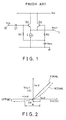
- FIG.1 shows a conventional detection circuit used in video signal processing apparatus for detecting video signals as it is for example disclosed in "Patent Abstract of Japan", Vol. 2, no. 56, 24th April 1978.
- a pair of npn transistors Q1 and Q2 are provided to form a differential amplifier. More specifically, the transistor Q1 has a collector connected to a voltage source V CC , an emitter connected to the ground via a constant current source I, and a base connected to an input terminal 10 via a coupling capacitor C1.
- the transistor Q2 has a collector connected commonly with the collector of the transistor Q1 to the voltage source V CC , an emitter connected, commonly with the emitter of the transistor Q1 to the ground via the constant current source I.
- the base of the transistor Q1 is biased by a reference voltage source V REF via a resistor R1.
- the transistor Q2 has a base biased by the same reference voltage source V REF via a resistor R2.
- the output of the detection circuit is obtained at an output terminal 11 which is connected to the emitter of the transistor Q1.
- the transistors Q1 and Q2 are biased to produce a constant output at the output terminal 11 as long as the input signal at the input terminal 10 is below a predetermined bias voltage level.
- the voltage level at the base of the transistor Q1 is changed positively and negatively about the bias voltage level.
- only the positive half cycle of the radio frequency signal is passed through the transistor Q1 from the base to the emitter after rectification at a p-n junction formed between the base and the emitter of the transistor Q1, and supplied to the output terminal 11.
- the output at the output terminal 11 remains stationary because of the rectifying action of the p-n junction.
- FIG.2 shows the operational characteristic of the detection circuit of FIG.1 which shows the input versus output characteristic for the input signal V in in the vicinity of the bias voltage represented by V B .
- the output of the detection circuit increases generally linearly when the voltage level in the input signal exceeds the predetermined bias voltage to the transistor Q1 while remains substantially stationary when the voltage level in the input signal is below the predetermined bias voltage.
- the input signal at the input terminal 10 is rectified and the detection of the amplitude modulated signal is achieved.
- an amplifier circuit is usually provided before the detection circuit for amplifying the input radio frequency signal so that the effect of the distortion is minimized.
- a measure is not desirable, as such an amplification at the earlier stages in the processing of signals may cause an unwanted saturation in the later stages. Thereby, an unwanted distortion is inevitably introduced.
- Another and more specific object of the present invention is to provide a detection circuit of amplitude modulated signals, wherein deviation from the ideal characteristic is eliminated.
- Another object of the present invention is to provide a detection circuit of amplitude modulated signals wherein an output signal produced in response to one of first and second half cycles of the input amplitude modulated signal increases the magnitude linearly with increasing amplitude of the input amplitude modulated signal while remains substantially zero in response to the other of the first and second half cycles.
- Another object of the present invention is to provide a detection circuit of amplitude modulated signals, comprising an input terminal to which an amplitude signal is supplied; a first bipolar transistor having a base connected to the input terminal, a collector connected to a first voltage source, providing a first power voltage, and an emitter; a second bipolar transistor having a base, a collector connected to the first voltage source, and an emitter which is coupled commonly to the emitter of the first bipolar transistor; an output terminal connected commonly to the emitter of the first bipolar transistor and the emitter of the second bipolar transistor for providing an output signal; and biasing means connected to the base of the first bipolar transistor and to the base of the second bipolar transistor for biasing the first and second bipolar transistors; wherein the detection circuit comprises control means having an input terminal connected to the base of the first bipolar transistor for producing a control signal in response to the amplitude modulated signal supplied to the input terminal; and variable current source means having a first end connected to the emitters of the first and second bipolar transistors, and a
- the deviation in the detection characteristic from the ideal characteristic for the small amplitude input signal is effectively compensated by changing the current flowing through the variable current source means in correspondence to the small amplitude of the input signal.
- the variable current source provides a constant current.
- the output voltage increases linearly with increasing amplitude of the amplitude modulated signal from the zero amplitude to a large amplitude, while in the other of the first and second half cycles, the output voltage remains substantially constant irrespective of the amplitude of the input amplitude modulated signal.
- FIG.3 explains the principle of the present invention.
- the parts that are constructed identically to those in FIG.2 are given identical reference numerals and the description thereof will be omitted.
- the constant current source I of FIG.1 is replaced by a variable current source 22 which changes the current flowing therethrough in accordance with a control signal supplied thereto.
- the total emitter current which is the sum of the emitter current through the transistor Q1 and the emitter current through the transistor Q2 is changed.
- control unit 21 for detecting a difference in the voltage at the base of the transistor Q1 and the voltage at the base of the transistor Q2.
- the control unit 21 produces, in response to the detected voltage difference, a control signal supplied to the variable current source 22, and the variable current source 22 is controlled in response to the control signal.
- the control unit 21 provides the control signal as a control current I x
- the variable current source 22 changes the current according to a relation I - I x , wherein I stands for the current which is set at a constant level.
- I stands for the current which is set at a constant level.
- the current I corresponds to the current that the constant current source I of FIG.1 provides.
- FIG.4 shows the characteristic of the control unit 21 for controlling the variable current source 22.
- the control unit 21 changes the current I x , which is deprived of from the variable current source 22, such that the current I x increases with increasing amplitude of the input signal V in at the input terminal 10 in both the positive and negative directions.
- the aforesaid change in the current I x occurs in a range A of the input voltage V in , and this range A corresponds to the range A shown in FIG.1 wherein the non-linearity in the detection characteristic as well as the offset appear remarkably. Beyond the range A in FIG.4, the current I x is held constant.
- variable current source 22 changes the current according to I - I x as already described. Thereby, there occurs a decrease in the current passing through the transistors Q1 and Q2, and associated therewith, there appears an increase in the voltage at the output terminal 11. Thereby, the characteristic curve shown in FIG.2 by the broken line is shifted upwards in corresponding to the region A.
- the characteristic of FIG.4 By suitably choosing the characteristic of FIG.4, one can cancel the deviation from the ideal characteristic shown in FIG.2. It should be noted that the deviation is caused mainly in the region A of the input signal V in .
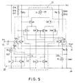
- the transistors Q1 and Q2 are connected similarly to the case of the circuit of FIG.3, and the description thereof, including the input terminal 10, the coupling capacitor C1, the bias resistance R1 and R2, the reference voltage source V REF , and the output terminal 11, will be omitted.
- an npn transistor Q3 such that the transistor Q3 has a base connected commonly to the base of the transistor Q1.
- npn transistor Q4 such that the transistor Q4 has a base connected commonly to the base of the transistor Q2.
- the transistors Q3 and Q4 have respective emitters connected commonly to the ground via a constant current source 120 that provides a constant current of 60 ⁇ A, for example.
- the transistors Q3 has a collector connected to the voltage source V CC via a level shift diode Q15 and a number of level shift diodes Q16, Q17, ..., for providing a voltage which is n times as large as the voltage V in , to respective bases of pnp transistors Q7 and Q10 to be described.
- the number n corresponds to the numbner of stages of the level shift diodes.
- the transistor Q4 has a collector connected to the voltage source V CC via the foregoing level shift diode Q15 and further via a number of level shift diodes Q18, Q19 for providing a voltage which is n times as large as a voltage -V in , to respective bases of pnp transistors Q8 and Q9.
- the transistors Q7 and Q8 have respective emitters connected commonly with each other, and these emitters are connected to a collector of a pnp transistor Q5.
- the transistors Q9 and Q10 similarly, have respective emitters connected commonly with each other, and these emitters are connected to a collector of a pnp transistor Q6.
- the transistor Q5 and Q6 have respective emitters connected commonly with each other, and these emitters are connected to the voltage source V CC via a constant current source 121 that provides a constant current I1 which may be 30 ⁇ A, for example. Further, the transistors Q5 and Q6 have respective bases such that the base of the transistor Q5 is connected to the collector of the transistor Q1 and the base of the transistor Q6 is connected to the collector of the transistor Q2. It should be noted that the collector of the transistor Q1 is connected, in this embodiment, to the voltage source V CC via a resistor R3 and the collector of the transistor Q2 is connected to the voltage source V CC via a resistor R4.
- the transistors Q7 and Q9 have respective collectors connected commonly with each other, and these collectors are connected to a collector of a transistor Q14 that is an npn transistor having a base connected to its collector.
- the transistors Q8 and Q10 have respective collectors connected commonly with each other to a collector of an npn transistor Q13.
- the transistor Q13 has a base connected to the base of the transistor Q14, and both the transistor Q13 and the transistor Q14 have respective emitters connected to the ground. Thereby, there is formed a current mirror circuit by the transistor Q13 and the transistor Q14.
- an npn transistor Q12 acting as the variable current source.
- the transistor Q12 has a collector connected to the emitter of the transistor Q1 and an emitter connected to the ground. Further, the transistor Q12 has a base connected to a base of an npn transistor Q11.
- the transistor Q11 has a collector connected to the voltage source V CC via a current source 122 and an emitter connected to the ground. Further, the base of the transistor Q11 is connected to its collector. It should be noted that the base of the transistor Q12 is connected to the collector of the transistor Q13 via a line 23 which corresponds to the line 23 shown in FIG.3.
- control unit 21 is constructed from the transistor Q3 - Q11, Q13 and Q14, and includes therein diodes Q15 - Q19 and constant current sources 120 - 122.
- variable current source 22 is formed from the transistor Q12 as already described.
- the collector current of the transistor Q1 and the collector current of the transistor Q3 are increased. For example, there appears an increase in the collector current of about 2 % in the transistor Q1 and Q3 in response to the increase of the voltage V in by about 1 mV.
- the collector current flowing through the transistor Q2 and the collector current flowing through the transistor Q4 are decreased by about 2 %.
- the voltage drop caused across the resistor R3 is increased by about 2 %, while the voltage drop caused across the resistor R4 is decreased by about 2 %, and the current supplied from the constant current source 121 is caused to flow mainly through the transistor Q5.
- such an increase in the collector current in the transistor Q3 induces an increase in the collector current of the transistor Q7 by about 4 % and a decrease in the collector current of the transistor Q8 by about 4 %.
- the collector current flowing through the transistor Q14 is increased with respect to the collector current flowing through the transistor Q13 by about 1.2 ⁇ A.
- the current corresponding to the difference has to be supplied from the current source 122 as the control current I x .
- the control current I x is diverted from the current I s that is provided by the constant current source 122, there naturally occurs a decrease in the collector currents flowing through the transistor Q11 and the transistor Q12.
- the collector current is decreased by about 1.2 ⁇ A.
- the voltage drop caused by the emitter resistance of the transistor Q1 is decreased by about 1 mV, and the base-emitter voltage V BE1 of the transistor Q1 is held constant irrespective of the increase in the input voltage V in .
- V out V in - V BE1 .
- the output voltage V out at the output terminal 11 is proportional to the input voltage V in and an excellent linearity is guaranteed even when the input amplitude modulated signal has a small amplitude.
- the collector current of the transistor Q1 and the collector current of the transistor Q3 are decreased by about 2 % while the collector current of the transistor Q2 and the collector current of the transistor Q4 are increased by about 2 %.
- the voltage drop across the resistor R3 is decreased by about 2 % while the voltage drop across the resistor R4 is increased by about 2 %.
- the increase in the collector current of the transistor Q4 causes an increase in the collector current of the transistor Q10 by about 4 % as well as a decrease in the collector current of the transistor Q9 by about 4%.
- the collector current of the transistor Q14 is set to be smaller than the collector current of the transistor Q13 by about 1.2 ⁇ A.
- this difference in the collector currents causes the control current I x to flow through the transistor Q11, together with the current I s from the constant current source 122.
- the collector current flowing through the transistor Q11 and the controller current flowing through the transistor Q12 are increased by about 1.2 ⁇ A, and the voltage drop caused by the emitter resistance of the transistor Q1 is increased by about 1.0 mV.
- the base-emitter voltage of the transistor Q1 is held constant even when there is a decrease in the input voltage V in from the bias voltage V B . In other words, the offset shown in FIG.2 is eliminated.
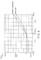
- FIG.6 shows an example of the compensation of the detection circuit achieved by the circuit of FIG.5. It will be seen from this drawing that the deviation from the ideal characteristic is substantially eliminated by suitably adjusting the parameters. On the other hand, when the setting of the parameters is inappropriate, there will be a case in which the deviation becomes even larger. The appropriate setting of the parameters can be found easily by performing the simulation of the circuit.
- control of the current I X for the compensation of deviation of the detection characteristic is not limited to the analog circuit as disclosed in FIG.5, but may be performed by digital means.
- the control unit 21 may be a digital processor that changes the current I X in response to the base voltage of the transistors Q1 and Q2 according to a predetermined program.
Description
- The present invention generally relates to detection circuits and more particularly to a detection circuit for detecting amplitude modulated signals.
- Detection circuits for detecting amplitude modulated signals are used in various electronic devices. In the simplest case, the detection circuit comprises a single diode. In the case of the detection of video signals and the like, a detection circuit that provides a particularly stable detection characteristic is required.
- FIG.1 shows a conventional detection circuit used in video signal processing apparatus for detecting video signals as it is for example disclosed in "Patent Abstract of Japan", Vol. 2, no. 56, 24th April 1978.
- Referring to FIG.1, a pair of npn transistors Q₁ and Q₂ are provided to form a differential amplifier. More specifically, the transistor Q₁ has a collector connected to a voltage source VCC, an emitter connected to the ground via a constant current source I, and a base connected to an
input terminal 10 via a coupling capacitor C1. The transistor Q₂ has a collector connected commonly with the collector of the transistor Q₁ to the voltage source VCC, an emitter connected, commonly with the emitter of the transistor Q₁ to the ground via the constant current source I. Further, the base of the transistor Q₁ is biased by a reference voltage source VREF via a resistor R₁. Similarly, the transistor Q₂ has a base biased by the same reference voltage source VREF via a resistor R₂. The output of the detection circuit is obtained at anoutput terminal 11 which is connected to the emitter of the transistor Q₁. - In operation, the transistors Q₁ and Q₂ are biased to produce a constant output at the
output terminal 11 as long as the input signal at theinput terminal 10 is below a predetermined bias voltage level. When there is an amplitude modulated radio frequency signal coming in at theinput terminal 10, the voltage level at the base of the transistor Q₁ is changed positively and negatively about the bias voltage level. Thereby, only the positive half cycle of the radio frequency signal is passed through the transistor Q₁ from the base to the emitter after rectification at a p-n junction formed between the base and the emitter of the transistor Q₁, and supplied to theoutput terminal 11. In the case that the radio frequency signal is in the negative half cycle, the output at theoutput terminal 11 remains stationary because of the rectifying action of the p-n junction. - FIG.2 shows the operational characteristic of the detection circuit of FIG.1 which shows the input versus output characteristic for the input signal Vin in the vicinity of the bias voltage represented by VB.
- Referring to FIG.1, the output of the detection circuit increases generally linearly when the voltage level in the input signal exceeds the predetermined bias voltage to the transistor Q₁ while remains substantially stationary when the voltage level in the input signal is below the predetermined bias voltage. Thereby, the input signal at the
input terminal 10 is rectified and the detection of the amplitude modulated signal is achieved. - In such a circuit, however, there is a problem in that the actual characteristic illustrated in FIG.2 by a broken line is deviated from the ideal characteristic which is illustrated by a solid line. It should be noted that the ideal characteristic has a sharp deflection at the origin corresponding to the bias voltage VB and the output voltage at the
output terminal 11 increases linearly with increasing voltage level at theinput terminal 10. In the actual case, however, there is no such a sharp deflection in the characteristic but the characteristic is curved as illustrated schematically. This deviation is caused by the well known rectifying characteristic of the p-n junction formed between the base and the emitter of the transistor Q₁. - When there is such a deviation, the output signal obtained at the
output terminal 11 is inevitably distorted because of the non-linearity in the characteristic curve. Further, a small, negative output appears even when the input amplitude modulated signal is in the negative half cycle. It should be noted that such negative output should not appear in the rectified signal at theoutput terminal 11. Because the non-linearity in the rectifying characteristic is limited in the vicinity of the voltage VB at the base of the transistor Q₁, it should be noted that such a distortion appears particularly conspicuous when the amplitude of the input signal Vin at theinput terminal 10 is small. - In order to avoid the problem of distortion of the output signal of the detection circuit, an amplifier circuit is usually provided before the detection circuit for amplifying the input radio frequency signal so that the effect of the distortion is minimized. However, such a measure is not desirable, as such an amplification at the earlier stages in the processing of signals may cause an unwanted saturation in the later stages. Thereby, an unwanted distortion is inevitably introduced.
- It is much more desirable to detect the radio frequency signals prior to the amplification so that the problem of distortion caused by the amplification in the later stages is avoided. For this purpose, the distortion caused in the radio frequency signals of the minute amplitude due to the deviation in the detection characteristic as explained has to be eliminated.
- Accordingly, it is a general object of the present invention to provide a novel and useful detection circuit for detecting amplitude modulated signals, wherein the aforementioned problems are eliminated.
- Another and more specific object of the present invention is to provide a detection circuit of amplitude modulated signals, wherein deviation from the ideal characteristic is eliminated.
- Another object of the present invention is to provide a detection circuit of amplitude modulated signals wherein an output signal produced in response to one of first and second half cycles of the input amplitude modulated signal increases the magnitude linearly with increasing amplitude of the input amplitude modulated signal while remains substantially zero in response to the other of the first and second half cycles.
- Another object of the present invention is to provide a detection circuit of amplitude modulated signals, comprising an input terminal to which an amplitude signal is supplied; a first bipolar transistor having a base connected to the input terminal, a collector connected to a first voltage source, providing a first power voltage, and an emitter; a second bipolar transistor having a base, a collector connected to the first voltage source, and an emitter which is coupled commonly to the emitter of the first bipolar transistor; an output terminal connected commonly to the emitter of the first bipolar transistor and the emitter of the second bipolar transistor for providing an output signal; and biasing means connected to the base of the first bipolar transistor and to the base of the second bipolar transistor for biasing the first and second bipolar transistors; wherein the detection circuit comprises control means having an input terminal connected to the base of the first bipolar transistor for producing a control signal in response to the amplitude modulated signal supplied to the input terminal; and variable current source means having a first end connected to the emitters of the first and second bipolar transistors, and a second end connected to a second voltage source providing a second power voltage which is different from the first power voltage, for causing to flow therethrough a drive current to the second voltage source, the drive current being a sum of an emitter current flowed through the first bipolar transistor and an emitter current flowed through the second bipolar transistor, the variable current source means having an input terminal connected to the control means for receiving therefrom the control signal and controlling the drive current flowing therethrough in response to the control signal; wherein the control means produces a control current as the control signal such that the control current has a magnitude that changes with the amplitude of the amplitude modulated signal at the input terminal in a predetermined range of amplitude of the amplitude modulated signal and such that the control current remains constant irrespective of the amplitude of the amplitude modulated signal in range of the amplitude beyond the predetermined range and the variable current source means provides the drive current by subtracting the control current from the predetermined current, so that the control means control the variable current source by the control signal such that the output signal at the output terminal has a voltage level which increases linearly with increasing amplitude of the input amplitude modulated signal in one of positive and negative half cycles of the amplitude modulated signal and such that the output signal has a constant voltage level in the other of the positive and negative half cycles of the amplitude modulated signal.
- According to the present invention, the deviation in the detection characteristic from the ideal characteristic for the small amplitude input signal is effectively compensated by changing the current flowing through the variable current source means in correspondence to the small amplitude of the input signal. On the other hand, when the input amplitude modulated signal has a moderate or large amplitude, the variable current source provides a constant current. As a result, there appears an output voltage on the output terminal such that, during one of first and second half cycles of the amplitude modulated signal at the input terminal, the output voltage increases linearly with increasing amplitude of the amplitude modulated signal from the zero amplitude to a large amplitude, while in the other of the first and second half cycles, the output voltage remains substantially constant irrespective of the amplitude of the input amplitude modulated signal.
- Other objects and further features of the present invention will become apparent from the following detailed description when read in conjunction with the attached drawings.
-
- FIG.1 is a circuit diagram showing a conventional detection circuit based for detecting amplitude modulated signals;
- FIG.2 is a graph for explaining the problem pertinent to the conventional circuit of FIG.1;
- FIG.3 is a circuit diagram for explaining the principle of the present invention;
- FIG.4 is a circuit diagram for explaining the operation of the circuit of FIG.3;
- FIG.5 is a circuit diagram showing a first embodiment of the present invention; and
- FIG.6 is a graph showing the operational characteristic of the circuit of FIG.5.
- FIG.3 explains the principle of the present invention. In FIG.3, the parts that are constructed identically to those in FIG.2 are given identical reference numerals and the description thereof will be omitted.
- In the circuit of FIG.3, the constant current source I of FIG.1 is replaced by a variable
current source 22 which changes the current flowing therethrough in accordance with a control signal supplied thereto. In other words, the total emitter current, which is the sum of the emitter current through the transistor Q₁ and the emitter current through the transistor Q₂ is changed. - In order to control the variable
current source 22, there is provided acontrol unit 21 for detecting a difference in the voltage at the base of the transistor Q₁ and the voltage at the base of the transistor Q₂. Thecontrol unit 21 produces, in response to the detected voltage difference, a control signal supplied to the variablecurrent source 22, and the variablecurrent source 22 is controlled in response to the control signal. - In the illustrated circuit, the
control unit 21 provides the control signal as a control current Ix, and the variablecurrent source 22 changes the current according to a relation I - Ix, wherein I stands for the current which is set at a constant level. It should be noted that the current I corresponds to the current that the constant current source I of FIG.1 provides. With increasing current Ix, the current flowing through the variablecurrent source 22 is decreased, and accordingly, the voltage level at the emitters of the transistor Q₁ and Q₂, which is detected at theoutput terminal 11, is modified. - FIG.4 shows the characteristic of the
control unit 21 for controlling the variablecurrent source 22. - Referring to FIG.4, the
control unit 21 changes the current Ix, which is deprived of from the variablecurrent source 22, such that the current Ix increases with increasing amplitude of the input signal Vin at theinput terminal 10 in both the positive and negative directions. It should be noted that the aforesaid change in the current Ix occurs in a range A of the input voltage Vin, and this range A corresponds to the range A shown in FIG.1 wherein the non-linearity in the detection characteristic as well as the offset appear remarkably. Beyond the range A in FIG.4, the current Ix is held constant. - In response to the current Ix, the variable
current source 22 changes the current according to I - Ix as already described. Thereby, there occurs a decrease in the current passing through the transistors Q₁ and Q₂, and associated therewith, there appears an increase in the voltage at theoutput terminal 11. Thereby, the characteristic curve shown in FIG.2 by the broken line is shifted upwards in corresponding to the region A. By suitably choosing the characteristic of FIG.4, one can cancel the deviation from the ideal characteristic shown in FIG.2. It should be noted that the deviation is caused mainly in the region A of the input signal Vin. - Next, a first embodiment of the present invention will be described with reference to FIG.5.
- Referring to FIG.5, the transistors Q₁ and Q₂ are connected similarly to the case of the circuit of FIG.3, and the description thereof, including the
input terminal 10, the coupling capacitor C1, the bias resistance R1 and R2, the reference voltage source VREF, and theoutput terminal 11, will be omitted. - In the circuit of FIG.5, there is provided an npn transistor Q₃ such that the transistor Q₃ has a base connected commonly to the base of the transistor Q₁. Similarly, there is provided an npn transistor Q4 such that the transistor Q4 has a base connected commonly to the base of the transistor Q₂. The transistors Q₃ and Q₄ have respective emitters connected commonly to the ground via a constant
current source 120 that provides a constant current of 60 µA, for example. Further, the transistors Q₃ has a collector connected to the voltage source VCC via a level shift diode Q₁₅ and a number of level shift diodes Q₁₆, Q₁₇, ..., for providing a voltage which is n times as large as the voltage Vin, to respective bases of pnp transistors Q₇ and Q₁₀ to be described. Here, the number n corresponds to the numbner of stages of the level shift diodes. The transistor Q₄ has a collector connected to the voltage source VCC via the foregoing level shift diode Q₁₅ and further via a number of level shift diodes Q₁₈, Q₁₉ for providing a voltage which is n times as large as a voltage -Vin, to respective bases of pnp transistors Q₈ and Q₉. - The transistors Q₇ and Q₈ have respective emitters connected commonly with each other, and these emitters are connected to a collector of a pnp transistor Q₅. The transistors Q₉ and Q₁₀, similarly, have respective emitters connected commonly with each other, and these emitters are connected to a collector of a pnp transistor Q₆.
- The transistor Q₅ and Q₆ have respective emitters connected commonly with each other, and these emitters are connected to the voltage source VCC via a constant current source 121 that provides a constant current I₁ which may be 30 µA, for example. Further, the transistors Q₅ and Q₆ have respective bases such that the base of the transistor Q₅ is connected to the collector of the transistor Q₁ and the base of the transistor Q₆ is connected to the collector of the transistor Q₂. It should be noted that the collector of the transistor Q₁ is connected, in this embodiment, to the voltage source VCC via a resistor R₃ and the collector of the transistor Q₂ is connected to the voltage source VCC via a resistor R₄.
- Further, the transistors Q₇ and Q₉ have respective collectors connected commonly with each other, and these collectors are connected to a collector of a transistor Q₁₄ that is an npn transistor having a base connected to its collector. Similarly, the transistors Q₈ and Q₁₀ have respective collectors connected commonly with each other to a collector of an npn transistor Q₁₃. The transistor Q₁₃ has a base connected to the base of the transistor Q₁₄, and both the transistor Q₁₃ and the transistor Q₁₄ have respective emitters connected to the ground. Thereby, there is formed a current mirror circuit by the transistor Q₁₃ and the transistor Q₁₄.
- To the emitter of the transistor Q₁, there is provided an npn transistor Q₁₂ acting as the variable current source. The transistor Q₁₂ has a collector connected to the emitter of the transistor Q₁ and an emitter connected to the ground. Further, the transistor Q₁₂ has a base connected to a base of an npn transistor Q₁₁. The transistor Q₁₁ has a collector connected to the voltage source VCC via a
current source 122 and an emitter connected to the ground. Further, the base of the transistor Q₁₁ is connected to its collector. It should be noted that the base of the transistor Q₁₂ is connected to the collector of the transistor Q₁₃ via aline 23 which corresponds to theline 23 shown in FIG.3. - In the foregoing construction, it should be noted that the
control unit 21 is constructed from the transistor Q₃ - Q₁₁, Q₁₃ and Q₁₄, and includes therein diodes Q₁₅ - Q₁₉ and constant current sources 120 - 122. On the other hand, the variablecurrent source 22 is formed from the transistor Q₁₂ as already described. - Next, the operation of the circuit of FIG.5 will be examined.
- In response to an increase in the input voltage Vin at the
input terminal 10 in correspondence to the incoming of an amplitude modulated signal, the collector current of the transistor Q₁ and the collector current of the transistor Q₃ are increased. For example, there appears an increase in the collector current of about 2 % in the transistor Q₁ and Q₃ in response to the increase of the voltage Vin by about 1 mV. - In response to this, the collector current flowing through the transistor Q₂ and the collector current flowing through the transistor Q₄ are decreased by about 2 %. Thereby, the voltage drop caused across the resistor R3 is increased by about 2 %, while the voltage drop caused across the resistor R4 is decreased by about 2 %, and the current supplied from the constant current source 121 is caused to flow mainly through the transistor Q₅. Further, such an increase in the collector current in the transistor Q₃ induces an increase in the collector current of the transistor Q₇ by about 4 % and a decrease in the collector current of the transistor Q₈ by about 4 %.
- Under such circumstances, the collector current flowing through the transistor Q₁₄ is increased with respect to the collector current flowing through the transistor Q₁₃ by about 1.2 µA. The current corresponding to the difference has to be supplied from the
current source 122 as the control current Ix. When the control current Ix is diverted from the current Is that is provided by the constantcurrent source 122, there naturally occurs a decrease in the collector currents flowing through the transistor Q₁₁ and the transistor Q₁₂. In the foregoing case, the collector current is decreased by about 1.2 µA. In correspondence to this, the voltage drop caused by the emitter resistance of the transistor Q₁ is decreased by about 1 mV, and the base-emitter voltage VBE1 of the transistor Q₁ is held constant irrespective of the increase in the input voltage Vin. - The output voltage Vout at the
output terminal 11 is represented as
- Thus, the output voltage Vout at the
output terminal 11 is proportional to the input voltage Vin and an excellent linearity is guaranteed even when the input amplitude modulated signal has a small amplitude. - Next, the case is considered where the voltage level Vin at the
input terminal 10 is changed negatively by 1mV from the bias voltage VB. - When this occurs, the collector current of the transistor Q₁ and the collector current of the transistor Q₃ are decreased by about 2 % while the collector current of the transistor Q₂ and the collector current of the transistor Q₄ are increased by about 2 %. In response to this, the voltage drop across the resistor R₃ is decreased by about 2 % while the voltage drop across the resistor R₄ is increased by about 2 %. Thereby, the current from the constant current source 121 is caused to flow mainly through the transistor Q₆.
- Further, the increase in the collector current of the transistor Q₄ causes an increase in the collector current of the transistor Q₁₀ by about 4 % as well as a decrease in the collector current of the transistor Q₉ by about 4%. With this, the collector current of the transistor Q₁₄ is set to be smaller than the collector current of the transistor Q₁₃ by about 1.2 µA. Now, this difference in the collector currents causes the control current Ix to flow through the transistor Q₁₁, together with the current Is from the constant
current source 122. In response to this, the collector current flowing through the transistor Q₁₁ and the controller current flowing through the transistor Q₁₂ are increased by about 1.2 µA, and the voltage drop caused by the emitter resistance of the transistor Q₁ is increased by about 1.0 mV. As a result, the base-emitter voltage of the transistor Q₁ is held constant even when there is a decrease in the input voltage Vin from the bias voltage VB. In other words, the offset shown in FIG.2 is eliminated. - FIG.6 shows an example of the compensation of the detection circuit achieved by the circuit of FIG.5. It will be seen from this drawing that the deviation from the ideal characteristic is substantially eliminated by suitably adjusting the parameters. On the other hand, when the setting of the parameters is inappropriate, there will be a case in which the deviation becomes even larger. The appropriate setting of the parameters can be found easily by performing the simulation of the circuit.
- Further, it should be noted that the control of the current IX for the compensation of deviation of the detection characteristic is not limited to the analog circuit as disclosed in FIG.5, but may be performed by digital means. In other words, the
control unit 21 may be a digital processor that changes the current IX in response to the base voltage of the transistors Q₁ and Q₂ according to a predetermined program.
Claims (7)
- A detection circuit of amplitude modulated signals, comprising: an input terminal (10) to which an amplitude signal is supplied; a first bipolar transistor (Q₁) having a base connected to the input terminal, a collector connected to a first voltage source (VCC) providing a first power voltage, and an emitter; a second bipolar transistor (Q₂) having a base, a collector connected to the first voltage source, and an emitter which is coupled commonly to the emitter of the first bipolar transistor; an output terminal (11) connected commonly to the emitter of the first bipolar transistor and the emitter of the second bipolar transistor for providing an output signal; and biasing means (VREF, R₁, R₂) connected to the base of the first bipolar transistor and to the base of the second bipolar transistor for biasing the first and second bipolar transistors;
characterized in that
the detection circuit comprises:
control means (21) having an input terminal connected to the base of the first bipolar transistor for producing a control signal (IX) in response to the amplitude modulated signal supplied to the input terminal;
and variable current source means (22) having a first end connected to the emitters of the first and second bipolar transistors, and a second end connected to a second voltage source providing a second power voltage which is different from the first power voltage, for causing to flow therethrough a drive current to the second voltage source, said drive current being a sum of an emitter current flowed through the first bipolar transistor and an emitter current flowed through the second bipolar transistor, said variable current source means having an input terminal connected to the control means for receiving therefrom the control signal and controlling the drive current flowing therethrough in response to the control signal;
wherein said control means (21) produces a control current (IX) as the control signal such that the control current has a magnitude that changes with the amplitude of the amplitude modulated signal at the input terminal in a predetermined range (A) of amplitude of the amplitude modulated signal and such that the control current remains constant irrespective of the amplitude of the amplitude modulated signal in a range of the amplitude beyond the predetermined range and said variable current source means provides the drive current
(I- IX) by subtracting the control current from the predetermined current, said control means controlling said variable current source by said control signal such that the output signal at the output terminal has a voltage level which increases linearly with increasing amplitude of the input amplitude modulated signal in one of positive and negative half cycles of the amplitude modulated signal and such that the output signal has a constant voltage level in the other of the positive and negative half cycles of the amplitude modulated signal. - A detection circuit as claimed in claim 1
characterized in that said control means changes the control current generally linearly with the amplitude of the amplitude modulated signal in the predetermined range in both the positive and negative half cycles of the amplitude modulated signal at the input terminal. - A detection circuit as claimed in claim 1
characterized in that said first bipolar transistor (Q₁) includes a p-n junction between the base and the emitter, said p-n junction providing a curved rectifying characteristic for the amplitude modulated signals that have an amplitude smaller than a predetermined input voltage range, and said predetermined range (A) is determined to correspond to said input voltage range. - A detection circuit as claimed in claim 1
characterized in that said control means comprises a differential circuit having a first input terminal connected to the base of the first bipolar transistor (Q₁) and a second end connected to the base of the second bipolar transistor (Q₂) for detecting a voltage difference between the first and second input terminals, said control means producing the control signal in response to the detected voltage difference. - A detection circuit as claimed in claim 1
characterized in that said control means comprises:
a first resistance (R₃) provided between the collector of the first bipolar transistor (Q₁) and the first voltage source (VCC);
a second resistance (R₄) provided between the collector of the second bipolar transistor and the first voltage source;
a third bipolar transistor (Q₃) having a base connected commonly with the base of the first bipolar transistor to the input terminal, an emitter, and a collector connected to the first voltage source;
a fourth bipolar transistor (Q₄) having a base connected commonly with the base of the second bipolar transistor to the biasing means, an emitter connected commonly with the emitter of the third bipolar transistor, a collector connected to the first voltage source via second level shifting means;
first constant current source means (120) having a first end connected to the second voltage source and a second end connected to the emitters of the third bipolar transistor and the fourth bipolar transistor;
a fifth bipolar transistor (Q₅) having a base connected to the collector of the first bipolar transistor, an emitter, and a collector;
a sixth bipolar transistor (Q₆) having a base connected to the collector of the second bipolar transistor, an emitter connected to the emitter of the fifth bipolar transistor, and a collector;
a second constant current source (121) having a first end connected to the first voltage source and a second end connected to the emitters of the fifth and sixth bipolar transistors;
a seventh bipolar transistor (Q₇) having a base connected to the second end of the first level shifting means, an emitter connected to the collector of the fifth bipolar transistor, and a collector;
an eighth bipolar transistor (Q₈) having a base connected to the collector of the fourth bipolar transistor, an emitter connected commonly with the emitter of the seventh bipolar transistor, to the collector of the fifth bipolar transistor, and a collector;
a ninth bipolar transistor (Q₉) having a base connected commonly with the base of the eights bipolar transistor to the collector of the fourth bipolar transistor, an emitter connected to the collector of the sixth bipolar transistor, and a collector connected commonly with the collector of the seventh bipolar transistor;
a tenth bipolar transistor (Q₁₀) having a base connected commonly with the base of the seventh bipolar transistor to the collector of the third bipolar transistor, an emitter connected commonly with the emitter of the ninth bipolar transistor to the collector of the sixth bipolar transistor, and a collector that is connected commonly with the collector of the eighth bipolar transistor;
a third constant current source (122) having a first end connected to the first voltage source and a second end;
an eleventh bipolar transistor (Q₁₁) having a connector connected to the second end of the third current source, an emitter connected to the second voltage source, and a base connected to the collector of the eleventh bipolar transistor;
a twelfth bipolar transistor (Q₁₂) having a base connected to the base of the eleventh bipolar transistor, a collector connected to the emitter of the first bipolar transistor, and an emitter connected to the second voltage source;
a thirteenth bipolar transistor (Q₁₃) having a collector connected to the collectors of the eighths and tenth bipolar transistors and further connected to the second end of the third constant current source, a base, and an emitter connected to the second voltage source; and
a fourteenth bipolar transistor (Q₁₄) having a collector connected to the collectors of the seventh and ninth bipolar transistors, a base connected to the base of the thirteenth bipolar transistor and to the collector of the fourteenth bipolar transistor, and an emitter connected to the second voltage source. - A detection circuit as claimed in claim 5
characterized in that said third, fourth, eleventh, twelfth, thirteenth and fourteenth bipolar transistors comprise an npn type bipolar transistor, and said fifth, sixth, seventh, eighth, ninth and tenth bipolar transistors comprise a pnp type bipolar transistor. - A detection circuit as claimed in claim 1
characterized in that said control means (21) comprises a digital processing unit.
Applications Claiming Priority (2)
| Application Number | Priority Date | Filing Date | Title |
|---|---|---|---|
| JP248860/89 | 1989-09-25 | ||
| JP1248860A JP2533201B2 (en) | 1989-09-25 | 1989-09-25 | AM detection circuit |
Publications (3)
| Publication Number | Publication Date |
|---|---|
| EP0420128A2 EP0420128A2 (en) | 1991-04-03 |
| EP0420128A3 EP0420128A3 (en) | 1991-09-25 |
| EP0420128B1 true EP0420128B1 (en) | 1995-09-13 |
Family
ID=17184502
Family Applications (1)
| Application Number | Title | Priority Date | Filing Date |
|---|---|---|---|
| EP90118349A Expired - Lifetime EP0420128B1 (en) | 1989-09-25 | 1990-09-24 | Detection circuit for amplitude modulated signals |
Country Status (5)
| Country | Link |
|---|---|
| US (1) | US5126683A (en) |
| EP (1) | EP0420128B1 (en) |
| JP (1) | JP2533201B2 (en) |
| KR (1) | KR940000923B1 (en) |
| DE (1) | DE69022341D1 (en) |
Families Citing this family (7)
| Publication number | Priority date | Publication date | Assignee | Title |
|---|---|---|---|---|
| JP2681001B2 (en) * | 1994-08-31 | 1997-11-19 | 日本電気アイシーマイコンシステム株式会社 | Comparator circuit |
| EP0738041B1 (en) * | 1995-04-13 | 1998-06-24 | Hewlett-Packard GmbH | Electronic circuit comprising a comparator |
| US6785521B2 (en) * | 2001-03-21 | 2004-08-31 | Ericsson Inc. | System and method for current-mode amplitude modulation |
| US20080061842A1 (en) * | 2006-09-07 | 2008-03-13 | Micron Technology, Inc. | Circuit and method for detecting timed amplitude reduction of a signal relative to a threshold voltage |
| US7560959B2 (en) * | 2006-09-18 | 2009-07-14 | Micron Technology, Inc. | Absolute value peak differential voltage detector circuit and method |
| US7911236B2 (en) | 2006-11-22 | 2011-03-22 | Intel Mobile Communications GmbH | Detection circuit and detection method |
| US8619382B2 (en) * | 2012-04-20 | 2013-12-31 | Texas Instruments Incorporated | High speed, low power write current switching scheme for HDD preamplifier |
Family Cites Families (8)
| Publication number | Priority date | Publication date | Assignee | Title |
|---|---|---|---|---|
| SU628603A1 (en) * | 1975-08-06 | 1978-10-15 | Предприятие П/Я Р-6208 | Transistorized arrangement for detecting amplitude-modulated signals |
| JPS5231644A (en) * | 1975-09-05 | 1977-03-10 | Hitachi Ltd | Amplifying detector |
| JPS5320760A (en) * | 1976-08-10 | 1978-02-25 | Matsushita Electric Ind Co Ltd | Detection circuit |
| JPS53114341A (en) * | 1977-02-21 | 1978-10-05 | Matsushita Electric Ind Co Ltd | Wave detection circuit |
| JPS5552605A (en) * | 1978-10-11 | 1980-04-17 | Nec Corp | Detector circuit |
| US4250457A (en) * | 1979-03-05 | 1981-02-10 | Zenith Radio Corporation | Full wave rectifier envelope detector |
| JPS5646666A (en) * | 1979-09-25 | 1981-04-27 | Toshiba Corp | All wave rectifier circuit |
| JPS5737905A (en) * | 1980-08-14 | 1982-03-02 | Toshiba Corp | Envelope curve wave detecting circuit |
-
1989
- 1989-09-25 JP JP1248860A patent/JP2533201B2/en not_active Expired - Fee Related
-
1990
- 1990-09-24 DE DE69022341T patent/DE69022341D1/en not_active Expired - Lifetime
- 1990-09-24 EP EP90118349A patent/EP0420128B1/en not_active Expired - Lifetime
- 1990-09-25 KR KR1019900015162A patent/KR940000923B1/en not_active IP Right Cessation
- 1990-09-25 US US07/587,685 patent/US5126683A/en not_active Expired - Lifetime
Also Published As
| Publication number | Publication date |
|---|---|
| US5126683A (en) | 1992-06-30 |
| EP0420128A3 (en) | 1991-09-25 |
| JPH03110907A (en) | 1991-05-10 |
| KR910007234A (en) | 1991-04-30 |
| KR940000923B1 (en) | 1994-02-04 |
| DE69022341D1 (en) | 1995-10-19 |
| EP0420128A2 (en) | 1991-04-03 |
| JP2533201B2 (en) | 1996-09-11 |
Similar Documents
| Publication | Publication Date | Title |
|---|---|---|
| US5162678A (en) | Temperature compensation control circuit for exponential gain function of an agc amplifier | |
| US4442400A (en) | Voltage-to-current converting circuit | |
| EP0196906B1 (en) | Automatic gain control detection circuit | |
| EP0420128B1 (en) | Detection circuit for amplitude modulated signals | |
| US4587478A (en) | Temperature-compensated current source having current and voltage stabilizing circuits | |
| US3555402A (en) | Constant current temperature stabilized signal converter circuit | |
| US5371476A (en) | Amplifying circuit | |
| JPH04369107A (en) | Differential amplifier | |
| US3544882A (en) | Electric current range converting amplifier | |
| KR100191109B1 (en) | Gain control circuit | |
| KR970005289B1 (en) | Differential amplifier | |
| US4370608A (en) | Integrable conversion circuit for converting input voltage to output current or voltage | |
| US4945314A (en) | Amplifier arrangement with saturation detection | |
| US5534813A (en) | Anti-logarithmic converter with temperature compensation | |
| CA1301862C (en) | Logarithmic amplification circuit for obtaining output voltage corresponding to difference between logarithmically amplified values of two input currents | |
| US4513245A (en) | DC current detector | |
| US5977760A (en) | Bipolar operational transconductance amplifier and output circuit used therefor | |
| US4904860A (en) | Optical signal detection circuit with constant current sources | |
| KR100284964B1 (en) | Current source circuit | |
| US4047118A (en) | Transistor amplifier circuit | |
| JPS6251077B2 (en) | ||
| KR850000581B1 (en) | Circuit for converting single-ended input signals to a pair of differential output signals | |
| JPH0474887B2 (en) | ||
| JPH02135810A (en) | Gain control circuit | |
| JPS63159986A (en) | Multiplier |
Legal Events
| Date | Code | Title | Description |
|---|---|---|---|
| PUAI | Public reference made under article 153(3) epc to a published international application that has entered the european phase |
Free format text: ORIGINAL CODE: 0009012 |
|
| AK | Designated contracting states |
Kind code of ref document: A2 Designated state(s): DE FR GB NL |
|
| PUAL | Search report despatched |
Free format text: ORIGINAL CODE: 0009013 |
|
| AK | Designated contracting states |
Kind code of ref document: A3 Designated state(s): DE FR GB NL |
|
| 17P | Request for examination filed |
Effective date: 19911030 |
|
| 17Q | First examination report despatched |
Effective date: 19940218 |
|
| GRAA | (expected) grant |
Free format text: ORIGINAL CODE: 0009210 |
|
| AK | Designated contracting states |
Kind code of ref document: B1 Designated state(s): DE FR GB NL |
|
| PG25 | Lapsed in a contracting state [announced via postgrant information from national office to epo] |
Ref country code: NL Free format text: LAPSE BECAUSE OF NON-PAYMENT OF DUE FEES Effective date: 19950913 |
|
| PGFP | Annual fee paid to national office [announced via postgrant information from national office to epo] |
Ref country code: GB Payment date: 19950913 Year of fee payment: 6 |
|
| REF | Corresponds to: |
Ref document number: 69022341 Country of ref document: DE Date of ref document: 19951019 |
|
| PG25 | Lapsed in a contracting state [announced via postgrant information from national office to epo] |
Ref country code: DE Effective date: 19951214 |
|
| ET | Fr: translation filed | ||
| NLV1 | Nl: lapsed or annulled due to failure to fulfill the requirements of art. 29p and 29m of the patents act | ||
| PLBE | No opposition filed within time limit |
Free format text: ORIGINAL CODE: 0009261 |
|
| STAA | Information on the status of an ep patent application or granted ep patent |
Free format text: STATUS: NO OPPOSITION FILED WITHIN TIME LIMIT |
|
| 26N | No opposition filed | ||
| PG25 | Lapsed in a contracting state [announced via postgrant information from national office to epo] |
Ref country code: GB Effective date: 19960924 |
|
| GBPC | Gb: european patent ceased through non-payment of renewal fee |
Effective date: 19960924 |
|
| PGFP | Annual fee paid to national office [announced via postgrant information from national office to epo] |
Ref country code: FR Payment date: 20050823 Year of fee payment: 16 |
|
| REG | Reference to a national code |
Ref country code: FR Ref legal event code: ST Effective date: 20070531 |
|
| PG25 | Lapsed in a contracting state [announced via postgrant information from national office to epo] |
Ref country code: FR Free format text: LAPSE BECAUSE OF NON-PAYMENT OF DUE FEES Effective date: 20061002 |