EP0420128B1 - Detektorschaltung für amplitudenmodulierte Signale - Google Patents
Detektorschaltung für amplitudenmodulierte Signale Download PDFInfo
- Publication number
- EP0420128B1 EP0420128B1 EP90118349A EP90118349A EP0420128B1 EP 0420128 B1 EP0420128 B1 EP 0420128B1 EP 90118349 A EP90118349 A EP 90118349A EP 90118349 A EP90118349 A EP 90118349A EP 0420128 B1 EP0420128 B1 EP 0420128B1
- Authority
- EP
- European Patent Office
- Prior art keywords
- bipolar transistor
- collector
- emitter
- base
- transistor
- Prior art date
- Legal status (The legal status is an assumption and is not a legal conclusion. Google has not performed a legal analysis and makes no representation as to the accuracy of the status listed.)
- Expired - Lifetime
Links
Images

Classifications
-
- H—ELECTRICITY
- H03—ELECTRONIC CIRCUITRY
- H03D—DEMODULATION OR TRANSFERENCE OF MODULATION FROM ONE CARRIER TO ANOTHER
- H03D1/00—Demodulation of amplitude-modulated oscillations
- H03D1/14—Demodulation of amplitude-modulated oscillations by means of non-linear elements having more than two poles
- H03D1/18—Demodulation of amplitude-modulated oscillations by means of non-linear elements having more than two poles of semiconductor devices
Definitions
- the present invention generally relates to detection circuits and more particularly to a detection circuit for detecting amplitude modulated signals.
- Detection circuits for detecting amplitude modulated signals are used in various electronic devices.
- the detection circuit comprises a single diode.
- a detection circuit that provides a particularly stable detection characteristic is required.
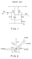
- FIG.1 shows a conventional detection circuit used in video signal processing apparatus for detecting video signals as it is for example disclosed in "Patent Abstract of Japan", Vol. 2, no. 56, 24th April 1978.
- a pair of npn transistors Q1 and Q2 are provided to form a differential amplifier. More specifically, the transistor Q1 has a collector connected to a voltage source V CC , an emitter connected to the ground via a constant current source I, and a base connected to an input terminal 10 via a coupling capacitor C1.
- the transistor Q2 has a collector connected commonly with the collector of the transistor Q1 to the voltage source V CC , an emitter connected, commonly with the emitter of the transistor Q1 to the ground via the constant current source I.
- the base of the transistor Q1 is biased by a reference voltage source V REF via a resistor R1.
- the transistor Q2 has a base biased by the same reference voltage source V REF via a resistor R2.
- the output of the detection circuit is obtained at an output terminal 11 which is connected to the emitter of the transistor Q1.
- the transistors Q1 and Q2 are biased to produce a constant output at the output terminal 11 as long as the input signal at the input terminal 10 is below a predetermined bias voltage level.
- the voltage level at the base of the transistor Q1 is changed positively and negatively about the bias voltage level.
- only the positive half cycle of the radio frequency signal is passed through the transistor Q1 from the base to the emitter after rectification at a p-n junction formed between the base and the emitter of the transistor Q1, and supplied to the output terminal 11.
- the output at the output terminal 11 remains stationary because of the rectifying action of the p-n junction.
- FIG.2 shows the operational characteristic of the detection circuit of FIG.1 which shows the input versus output characteristic for the input signal V in in the vicinity of the bias voltage represented by V B .
- the output of the detection circuit increases generally linearly when the voltage level in the input signal exceeds the predetermined bias voltage to the transistor Q1 while remains substantially stationary when the voltage level in the input signal is below the predetermined bias voltage.
- the input signal at the input terminal 10 is rectified and the detection of the amplitude modulated signal is achieved.
- an amplifier circuit is usually provided before the detection circuit for amplifying the input radio frequency signal so that the effect of the distortion is minimized.
- a measure is not desirable, as such an amplification at the earlier stages in the processing of signals may cause an unwanted saturation in the later stages. Thereby, an unwanted distortion is inevitably introduced.
- Another and more specific object of the present invention is to provide a detection circuit of amplitude modulated signals, wherein deviation from the ideal characteristic is eliminated.
- Another object of the present invention is to provide a detection circuit of amplitude modulated signals wherein an output signal produced in response to one of first and second half cycles of the input amplitude modulated signal increases the magnitude linearly with increasing amplitude of the input amplitude modulated signal while remains substantially zero in response to the other of the first and second half cycles.
- Another object of the present invention is to provide a detection circuit of amplitude modulated signals, comprising an input terminal to which an amplitude signal is supplied; a first bipolar transistor having a base connected to the input terminal, a collector connected to a first voltage source, providing a first power voltage, and an emitter; a second bipolar transistor having a base, a collector connected to the first voltage source, and an emitter which is coupled commonly to the emitter of the first bipolar transistor; an output terminal connected commonly to the emitter of the first bipolar transistor and the emitter of the second bipolar transistor for providing an output signal; and biasing means connected to the base of the first bipolar transistor and to the base of the second bipolar transistor for biasing the first and second bipolar transistors; wherein the detection circuit comprises control means having an input terminal connected to the base of the first bipolar transistor for producing a control signal in response to the amplitude modulated signal supplied to the input terminal; and variable current source means having a first end connected to the emitters of the first and second bipolar transistors, and a
- the deviation in the detection characteristic from the ideal characteristic for the small amplitude input signal is effectively compensated by changing the current flowing through the variable current source means in correspondence to the small amplitude of the input signal.
- the variable current source provides a constant current.
- the output voltage increases linearly with increasing amplitude of the amplitude modulated signal from the zero amplitude to a large amplitude, while in the other of the first and second half cycles, the output voltage remains substantially constant irrespective of the amplitude of the input amplitude modulated signal.
- FIG.3 explains the principle of the present invention.
- the parts that are constructed identically to those in FIG.2 are given identical reference numerals and the description thereof will be omitted.
- the constant current source I of FIG.1 is replaced by a variable current source 22 which changes the current flowing therethrough in accordance with a control signal supplied thereto.
- the total emitter current which is the sum of the emitter current through the transistor Q1 and the emitter current through the transistor Q2 is changed.
- control unit 21 for detecting a difference in the voltage at the base of the transistor Q1 and the voltage at the base of the transistor Q2.
- the control unit 21 produces, in response to the detected voltage difference, a control signal supplied to the variable current source 22, and the variable current source 22 is controlled in response to the control signal.
- the control unit 21 provides the control signal as a control current I x
- the variable current source 22 changes the current according to a relation I - I x , wherein I stands for the current which is set at a constant level.
- I stands for the current which is set at a constant level.
- the current I corresponds to the current that the constant current source I of FIG.1 provides.
- FIG.4 shows the characteristic of the control unit 21 for controlling the variable current source 22.
- the control unit 21 changes the current I x , which is deprived of from the variable current source 22, such that the current I x increases with increasing amplitude of the input signal V in at the input terminal 10 in both the positive and negative directions.
- the aforesaid change in the current I x occurs in a range A of the input voltage V in , and this range A corresponds to the range A shown in FIG.1 wherein the non-linearity in the detection characteristic as well as the offset appear remarkably. Beyond the range A in FIG.4, the current I x is held constant.
- variable current source 22 changes the current according to I - I x as already described. Thereby, there occurs a decrease in the current passing through the transistors Q1 and Q2, and associated therewith, there appears an increase in the voltage at the output terminal 11. Thereby, the characteristic curve shown in FIG.2 by the broken line is shifted upwards in corresponding to the region A.
- the characteristic of FIG.4 By suitably choosing the characteristic of FIG.4, one can cancel the deviation from the ideal characteristic shown in FIG.2. It should be noted that the deviation is caused mainly in the region A of the input signal V in .
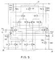
- the transistors Q1 and Q2 are connected similarly to the case of the circuit of FIG.3, and the description thereof, including the input terminal 10, the coupling capacitor C1, the bias resistance R1 and R2, the reference voltage source V REF , and the output terminal 11, will be omitted.
- an npn transistor Q3 such that the transistor Q3 has a base connected commonly to the base of the transistor Q1.
- npn transistor Q4 such that the transistor Q4 has a base connected commonly to the base of the transistor Q2.
- the transistors Q3 and Q4 have respective emitters connected commonly to the ground via a constant current source 120 that provides a constant current of 60 ⁇ A, for example.
- the transistors Q3 has a collector connected to the voltage source V CC via a level shift diode Q15 and a number of level shift diodes Q16, Q17, ..., for providing a voltage which is n times as large as the voltage V in , to respective bases of pnp transistors Q7 and Q10 to be described.
- the number n corresponds to the numbner of stages of the level shift diodes.
- the transistor Q4 has a collector connected to the voltage source V CC via the foregoing level shift diode Q15 and further via a number of level shift diodes Q18, Q19 for providing a voltage which is n times as large as a voltage -V in , to respective bases of pnp transistors Q8 and Q9.
- the transistors Q7 and Q8 have respective emitters connected commonly with each other, and these emitters are connected to a collector of a pnp transistor Q5.
- the transistors Q9 and Q10 similarly, have respective emitters connected commonly with each other, and these emitters are connected to a collector of a pnp transistor Q6.
- the transistor Q5 and Q6 have respective emitters connected commonly with each other, and these emitters are connected to the voltage source V CC via a constant current source 121 that provides a constant current I1 which may be 30 ⁇ A, for example. Further, the transistors Q5 and Q6 have respective bases such that the base of the transistor Q5 is connected to the collector of the transistor Q1 and the base of the transistor Q6 is connected to the collector of the transistor Q2. It should be noted that the collector of the transistor Q1 is connected, in this embodiment, to the voltage source V CC via a resistor R3 and the collector of the transistor Q2 is connected to the voltage source V CC via a resistor R4.
- the transistors Q7 and Q9 have respective collectors connected commonly with each other, and these collectors are connected to a collector of a transistor Q14 that is an npn transistor having a base connected to its collector.
- the transistors Q8 and Q10 have respective collectors connected commonly with each other to a collector of an npn transistor Q13.
- the transistor Q13 has a base connected to the base of the transistor Q14, and both the transistor Q13 and the transistor Q14 have respective emitters connected to the ground. Thereby, there is formed a current mirror circuit by the transistor Q13 and the transistor Q14.
- an npn transistor Q12 acting as the variable current source.
- the transistor Q12 has a collector connected to the emitter of the transistor Q1 and an emitter connected to the ground. Further, the transistor Q12 has a base connected to a base of an npn transistor Q11.
- the transistor Q11 has a collector connected to the voltage source V CC via a current source 122 and an emitter connected to the ground. Further, the base of the transistor Q11 is connected to its collector. It should be noted that the base of the transistor Q12 is connected to the collector of the transistor Q13 via a line 23 which corresponds to the line 23 shown in FIG.3.
- control unit 21 is constructed from the transistor Q3 - Q11, Q13 and Q14, and includes therein diodes Q15 - Q19 and constant current sources 120 - 122.
- variable current source 22 is formed from the transistor Q12 as already described.
- the collector current of the transistor Q1 and the collector current of the transistor Q3 are increased. For example, there appears an increase in the collector current of about 2 % in the transistor Q1 and Q3 in response to the increase of the voltage V in by about 1 mV.
- the collector current flowing through the transistor Q2 and the collector current flowing through the transistor Q4 are decreased by about 2 %.
- the voltage drop caused across the resistor R3 is increased by about 2 %, while the voltage drop caused across the resistor R4 is decreased by about 2 %, and the current supplied from the constant current source 121 is caused to flow mainly through the transistor Q5.
- such an increase in the collector current in the transistor Q3 induces an increase in the collector current of the transistor Q7 by about 4 % and a decrease in the collector current of the transistor Q8 by about 4 %.
- the collector current flowing through the transistor Q14 is increased with respect to the collector current flowing through the transistor Q13 by about 1.2 ⁇ A.
- the current corresponding to the difference has to be supplied from the current source 122 as the control current I x .
- the control current I x is diverted from the current I s that is provided by the constant current source 122, there naturally occurs a decrease in the collector currents flowing through the transistor Q11 and the transistor Q12.
- the collector current is decreased by about 1.2 ⁇ A.
- the voltage drop caused by the emitter resistance of the transistor Q1 is decreased by about 1 mV, and the base-emitter voltage V BE1 of the transistor Q1 is held constant irrespective of the increase in the input voltage V in .
- V out V in - V BE1 .
- the output voltage V out at the output terminal 11 is proportional to the input voltage V in and an excellent linearity is guaranteed even when the input amplitude modulated signal has a small amplitude.
- the collector current of the transistor Q1 and the collector current of the transistor Q3 are decreased by about 2 % while the collector current of the transistor Q2 and the collector current of the transistor Q4 are increased by about 2 %.
- the voltage drop across the resistor R3 is decreased by about 2 % while the voltage drop across the resistor R4 is increased by about 2 %.
- the increase in the collector current of the transistor Q4 causes an increase in the collector current of the transistor Q10 by about 4 % as well as a decrease in the collector current of the transistor Q9 by about 4%.
- the collector current of the transistor Q14 is set to be smaller than the collector current of the transistor Q13 by about 1.2 ⁇ A.
- this difference in the collector currents causes the control current I x to flow through the transistor Q11, together with the current I s from the constant current source 122.
- the collector current flowing through the transistor Q11 and the controller current flowing through the transistor Q12 are increased by about 1.2 ⁇ A, and the voltage drop caused by the emitter resistance of the transistor Q1 is increased by about 1.0 mV.
- the base-emitter voltage of the transistor Q1 is held constant even when there is a decrease in the input voltage V in from the bias voltage V B . In other words, the offset shown in FIG.2 is eliminated.
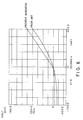
- FIG.6 shows an example of the compensation of the detection circuit achieved by the circuit of FIG.5. It will be seen from this drawing that the deviation from the ideal characteristic is substantially eliminated by suitably adjusting the parameters. On the other hand, when the setting of the parameters is inappropriate, there will be a case in which the deviation becomes even larger. The appropriate setting of the parameters can be found easily by performing the simulation of the circuit.
- control of the current I X for the compensation of deviation of the detection characteristic is not limited to the analog circuit as disclosed in FIG.5, but may be performed by digital means.
- the control unit 21 may be a digital processor that changes the current I X in response to the base voltage of the transistors Q1 and Q2 according to a predetermined program.
Landscapes
- Physics & Mathematics (AREA)
- Nonlinear Science (AREA)
- Engineering & Computer Science (AREA)
- Power Engineering (AREA)
- Amplifiers (AREA)
- Amplitude Modulation (AREA)
- Measurement Of Current Or Voltage (AREA)
Claims (7)
- Detektorschaltung für amplitudenmodulierte Signale, umfassend:
einen Eingangsanschluß (10), an den ein Amplitudensignal angelegt ist,
einen ersten Bipolartransistor (Q₁) mit einer an den Eingangsanschluß angeschlossenen Basis, einem an eine eine erste Spannung liefernde Spannungsquelle (VCC) angeschlossenen Kollektor und mit einem Emitter,
einen zweiten Bipolartrasistor (Q₂) mit einer Basis, einem an die erste Spannungsquelle angeschlossenen Kollektor und einem mit dem Emitter des ersten Bipolartransistors verbundenen Emitter,
einen Ausgangsanschluß (11) zum Bereitstellen eines Ausgangssignals, welcher sowohl mit dem Emitter des ersten Bipolartrasistors als auch mit dem Emitter des zweiten Bipolartransistors verbunden ist, und
eine Vorspannungsvorrichtung (VREF, R₁, R₂) zum Vorspannen des ersten und zweiten Bipolartransistors, welche sowohl mit der Basis des ersten Bipolartransistors als auch mit der Basis des zweiten Bipolartransistors verbunden ist,
dadurch gekennzeichnet,
daß die Detektorschaltung weiterhin umfaßt:
eine Steuervorrichtung (21) mit einem mit der Basis des ersten Bipolartransistors verbundenen Eingangsanschluß, welche abhängig von dem an den Eingangsanschluß angelegten amplitudenmodulierten Signal ein Steuersignal (IX) erzeugt, und eine veränderbare Stromquellenvorrichtung (22) mit einem mit den Emittern des ersten und zweiten Bipolartransistors verbundenen ersten Ende und mit einem mit einer zweiten Spannungsquelle zum Bereitstellen einer von der ersten Spannung verschiedenen zweiten Spannung verbundenen zweiten Ende, damit zu der zweiten Spannungsquelle ein Treiberstrom fließen kann, welcher die Summe eines durch den ersten Bipolartransistor fließenden Emitterstroms und eines durch den zweiten Bipolartransistor fließenden Emitterstroms ist, wobei die veränderbare Stromquellenvorrichtung einen mit der Steuervorrichtung verbundenen Eingangsanschluß aufweist, um von der Steuervorrichtung das Steuersignal zu empfangen und abhängig von dem Steuersignal den hindurchfließenden Treiberstrom zu steuern,
wobei die Steuervorrichtung (21) einen Steuerstrom (IX) als das Steuersignal derart erzeugt, daß der Steuerstrom eine sich in einem bestimmten Amplitudenbereich (A) des amplitudenmodulierten Signals mit der Amplitude des an dem Eingangsanschluß bereitgestellten amplitudenmodulierten Signals verändernde Größenordnung aufweist,
und daß der Steuerstrom unabhängig von der Amplitude des amplitudenmodulierten Signals in einem außerhalb des bestimmten Bereichs liegenden Amplitudenbereich konstant ist, und
wobei die veränderbare Stromquellenvorrichtung den Treiberstrom (I-IX) durch Subtrahieren des Steuerstromes von dem bestimmten Strom bereitstellt und von der Steuervorrichtung mittels des Steuersignals derart gesteuert wird, daß das Ausgangssignal an dem Ausgangsanschluß einen Spannungspegel aufweist, der entweder in der positiven oder negativen Halbwelle des amplitudenmodulierten Signals linear mit der ansteigenden Amplitude des amplitudenmodulierten Eingangssignals ansteigt und in der anderen Halbwelle des amplitudenmodulierten Signals konstant ist. - Detektorschaltung nach Anspruch 2,
dadurch gekennzeichnet,
daß die Steuervorrichtung den Steuerstrom im wesentlichen linear mit der Amplitude des amplitudenmodulierten Signals in dem bestimmten Bereich sowohl für die positiven als auch für die negativen Halbwellen des an dem Eingangsanschluß anliegenden amplitudenmodulierten Signals verändert. - Detektorschaltung nach Anspruch 1,
dadurch gekennzeichnet,
daß der erste Bipolartransistor (Q₁) einen pn-Übergang zwischen der Basis und dem Emitter aufweist, welcher eine kurvenförmige Gleichrichtercharakteristik für die amplitudenmodulierten Signale aufweist, deren Amplitude kleiner als ein bestimmter Eingangsspannungsbereich ist, und
daß der bestimmte Bereich (A) entsprechend dem Eingangsspannungsbereich festgelegt ist. - Detektorschaltung nach Anspruch 1,
dadurch gekennzeichnet,
daß die Steuervorrichtung eine Differenzschaltung mit einem mit der Basis des ersten Bipolartransistors (Q₁) verbundenen ersten Eingangsanschluß und einem mit der Basis des zweiten Bipolartransistors (Q₂) verbundenen zweiten Eingangsanschluß aufweist,
zum Erfassen einer Spannungsdifferenz zwischen dem ersten und dem zweiten Eingangsanschluß, wobei die Steuerschaltung das Steuersignal abhängig von der erfaßten Spannungsdifferenz erzeugt. - Detektorschaltung nach Anspruch 1,
dadurch gekennzeichnet,
daß die Steuervorrichtung umfaßt:
einen zwischen dem Kollektor des ersten Bipolartransistors (Q₁) und der ersten Spannungsquelle (VCC) angeordneten ersten Widerstand (R₃),
einen zwischen dem Kollektor des zweiten Bipolartransistors (Q₂) und der ersten Spannungsquelle angeordneten zweiten Widerstand (R₄),
einen dritten Bipolartransistor (Q₃) mit einer mit der Basis des ersten Bipolartransistors an den Eingangsanschluß angeschlossenen Basis, einem Emitter und einem mit der ersten Spannungsquelle verbundenen Kollektor,
einen vierten Bipolartransistor (Q₄) mit einer mit der Basis des zweiten Bipolartransistors an die Vorspannungsvorrichtung angeschlossenen Basis, einem mit dem Emitter des dritten Bipolartransistors verbundenen Emitter und einem über eine zweite Pegelveränderungsvorrichtung an die erste Spannungsquelle angeschlossenen Kollektor,
eine erste Konstantstromquellenvorrichtung (120) mit einem an die zweite Spannungsquelle angeschlossenen ersten Ende und einem an die Emitter des dritten und vierten Bipolartransistors angeschlossenen zweiten Ende,
einen fünften Bipolartransistor (Q₅) mit einer an den Kollektor des ersten Bipolartransistors angeschlossenen Basis, einem Emitter und einem Kollektor,
einen sechsten Bipolartransistor (Q₆) mit einer an den Kollektor des zweiten Bipolartransistors angeschlossenen Basis, einem an den Emitter des fünften Bipolartransistors angeschlossenen Emitter und einem Kollektor,
eine zweite konstante Stromquellenvorrichtung (121) mit einem an die erste Spannungsquelle angeschlossenen ersten Ende und einem an die Emitter des fünften und sechsten Bipolartransistors angeschlossenen zweiten Ende,
einen siebten Bipolartransistor (Q₇) mit einer an das zweite Ende der ersten Pegelveränderungsvorrichtung angeschlossenen Basis, einem mit dem Kollektor des fünften Bipolartransistors verbundenen Emitter und einem Kollektor,
einen achten Bipolartransistor (Q₈) mit einer an den Kollektor des vierten Bipolartransistors angeschlossenen Basis, einem mit dem Emitter des siebten Bipolartransistors an den Kollektor des fünften Bipolartransistors angeschlossenen Emitter und einem Kollektor,
einen neunten Bipolartransistor (Q₉) mit einer mit der Basis des achten Bipolartransistors an den Kollektor des vierten Bipolartransistors angeschlossenen Basis,
einem an den Kollektor des sechsten Bipolartransistors angeschlossenen Emitter und einem mit dem Kollektor des siebten Bipolartransistors verbundenen Kollektor,
einen zehnten Bipolartransistor (Q₁₀) mit einer mit der Basis des siebten Bipolartransistors an den Kollektor des vierten Bipolartransistors angeschlossenen Basis,
einem mit dem Emitter des neunten Bipolatransistors an den Kollektor des sechsten Bipolartransistors angeschlossenen Emitter und einem mit dem Kollektor des achten Bipolartransistors verbundenen Kollektor,
einer dritten Konstantstromquellenvorrichtung (122) mit einem an die erste Spannungsquelle angeschlossenen ersten Ende und einem zweiten Ende,
einen elften Bipolartransistor (Q₁₁) mit einem an das zweite Ende der dritten Konstantstromquellenvorrichtung angeschlossenen Kollektor, einem mit der zweiten Spannungsquelle verbundenen Emitter und einer mit dem Kollektor des elften Bipolartransistors verbundenen Basis,
einen zwölften Bipolartransistor (Q₁₂) mit einer mit der Basis des elften Bipolartransistors verbundenen Basis, einem an den Emitter des ersten Bipolartransistors angeschlossenen Kollektor und einem an die zweite Spannungsquelle angeschlossenen Emitter,
einen dreizehnten Bipolartransistor (Q₁₃) mit einem an die Kollektoren des achten und zehnten Bipolartransistors und dem zweiten Ende der dritten Konstantstromquellenvorrichtung verbundenen Kollektor, einer Basis und einem mit der zweiten Spannungsquelle verbundenen Emitter, und
einen vierzehnten Bipolartransistor (Q₁₄) mit einem an die Kollektoren des siebten und neunten Bipolartransistors angeschlossenen Kollektor, einer mit der Basis des dreizehnten Bipolartransistors und dem Kollektor des vierzehnten Bipolartransistors verbundenen Basis und einem mit der zweiten Spannungsquelle verbundenen Emitter. - Detektorschaltung nach Anspruch 5,
dadurch gekennzeichnet,
daß der dritte, vierte, elfte, zwölfte, dreizehnte und vierzehnte Bipolartransistor ein npn-Bipolartransistor ist, und
daß der fünfte, sechste, siebte, achte, neunte und zehnte Bipolartransistor ein pnp-Bipolartransistor ist. - Detektorschaltung nach Anspruch 1,
dadurch gekennzeichnet,
daß die Steuervorrichtung (21) eine digitale Zentraleinheit umfaßt.
Applications Claiming Priority (2)
| Application Number | Priority Date | Filing Date | Title |
|---|---|---|---|
| JP1248860A JP2533201B2 (ja) | 1989-09-25 | 1989-09-25 | Am検波回路 |
| JP248860/89 | 1989-09-25 |
Publications (3)
| Publication Number | Publication Date |
|---|---|
| EP0420128A2 EP0420128A2 (de) | 1991-04-03 |
| EP0420128A3 EP0420128A3 (en) | 1991-09-25 |
| EP0420128B1 true EP0420128B1 (de) | 1995-09-13 |
Family
ID=17184502
Family Applications (1)
| Application Number | Title | Priority Date | Filing Date |
|---|---|---|---|
| EP90118349A Expired - Lifetime EP0420128B1 (de) | 1989-09-25 | 1990-09-24 | Detektorschaltung für amplitudenmodulierte Signale |
Country Status (5)
| Country | Link |
|---|---|
| US (1) | US5126683A (de) |
| EP (1) | EP0420128B1 (de) |
| JP (1) | JP2533201B2 (de) |
| KR (1) | KR940000923B1 (de) |
| DE (1) | DE69022341D1 (de) |
Families Citing this family (7)
| Publication number | Priority date | Publication date | Assignee | Title |
|---|---|---|---|---|
| JP2681001B2 (ja) * | 1994-08-31 | 1997-11-19 | 日本電気アイシーマイコンシステム株式会社 | コンパレータ回路 |
| EP0738041B1 (de) * | 1995-04-13 | 1998-06-24 | Hewlett-Packard GmbH | Einen Komparator enthaltende elektronische Schaltung |
| US6785521B2 (en) * | 2001-03-21 | 2004-08-31 | Ericsson Inc. | System and method for current-mode amplitude modulation |
| US20080061842A1 (en) * | 2006-09-07 | 2008-03-13 | Micron Technology, Inc. | Circuit and method for detecting timed amplitude reduction of a signal relative to a threshold voltage |
| US7560959B2 (en) * | 2006-09-18 | 2009-07-14 | Micron Technology, Inc. | Absolute value peak differential voltage detector circuit and method |
| US7911236B2 (en) | 2006-11-22 | 2011-03-22 | Intel Mobile Communications GmbH | Detection circuit and detection method |
| US8619382B2 (en) * | 2012-04-20 | 2013-12-31 | Texas Instruments Incorporated | High speed, low power write current switching scheme for HDD preamplifier |
Family Cites Families (8)
| Publication number | Priority date | Publication date | Assignee | Title |
|---|---|---|---|---|
| SU628603A1 (ru) * | 1975-08-06 | 1978-10-15 | Предприятие П/Я Р-6208 | Устройство дл детектировани амплитудно-модулированных сигналов |
| JPS5231644A (en) * | 1975-09-05 | 1977-03-10 | Hitachi Ltd | Amplifying detector |
| JPS5320760A (en) * | 1976-08-10 | 1978-02-25 | Matsushita Electric Ind Co Ltd | Detection circuit |
| JPS53114341A (en) * | 1977-02-21 | 1978-10-05 | Matsushita Electric Ind Co Ltd | Wave detection circuit |
| JPS5552605A (en) * | 1978-10-11 | 1980-04-17 | Nec Corp | Detector circuit |
| US4250457A (en) * | 1979-03-05 | 1981-02-10 | Zenith Radio Corporation | Full wave rectifier envelope detector |
| JPS5646666A (en) * | 1979-09-25 | 1981-04-27 | Toshiba Corp | All wave rectifier circuit |
| JPS5737905A (en) * | 1980-08-14 | 1982-03-02 | Toshiba Corp | Envelope curve wave detecting circuit |
-
1989
- 1989-09-25 JP JP1248860A patent/JP2533201B2/ja not_active Expired - Fee Related
-
1990
- 1990-09-24 EP EP90118349A patent/EP0420128B1/de not_active Expired - Lifetime
- 1990-09-24 DE DE69022341T patent/DE69022341D1/de not_active Expired - Lifetime
- 1990-09-25 US US07/587,685 patent/US5126683A/en not_active Expired - Lifetime
- 1990-09-25 KR KR1019900015162A patent/KR940000923B1/ko not_active IP Right Cessation
Also Published As
| Publication number | Publication date |
|---|---|
| EP0420128A3 (en) | 1991-09-25 |
| KR940000923B1 (ko) | 1994-02-04 |
| DE69022341D1 (de) | 1995-10-19 |
| JPH03110907A (ja) | 1991-05-10 |
| KR910007234A (ko) | 1991-04-30 |
| US5126683A (en) | 1992-06-30 |
| EP0420128A2 (de) | 1991-04-03 |
| JP2533201B2 (ja) | 1996-09-11 |
Similar Documents
| Publication | Publication Date | Title |
|---|---|---|
| US5162678A (en) | Temperature compensation control circuit for exponential gain function of an agc amplifier | |
| US4442400A (en) | Voltage-to-current converting circuit | |
| EP0196906B1 (de) | Schaltung zur Detektion eines automatischen Verstärkungsregelungssignals | |
| EP0420128B1 (de) | Detektorschaltung für amplitudenmodulierte Signale | |
| US4587478A (en) | Temperature-compensated current source having current and voltage stabilizing circuits | |
| US3555402A (en) | Constant current temperature stabilized signal converter circuit | |
| US5371476A (en) | Amplifying circuit | |
| JPH04369107A (ja) | 差動増幅器 | |
| US3544882A (en) | Electric current range converting amplifier | |
| KR100191109B1 (ko) | 서보회로 | |
| KR970005289B1 (ko) | 차동 증폭기 | |
| US4370608A (en) | Integrable conversion circuit for converting input voltage to output current or voltage | |
| US4945314A (en) | Amplifier arrangement with saturation detection | |
| US5534813A (en) | Anti-logarithmic converter with temperature compensation | |
| CA1301862C (en) | Logarithmic amplification circuit for obtaining output voltage corresponding to difference between logarithmically amplified values of two input currents | |
| US4513245A (en) | DC current detector | |
| US5977760A (en) | Bipolar operational transconductance amplifier and output circuit used therefor | |
| US4904860A (en) | Optical signal detection circuit with constant current sources | |
| KR100284964B1 (ko) | 전류원 회로 | |
| US4047118A (en) | Transistor amplifier circuit | |
| JPS6251077B2 (de) | ||
| KR850000581B1 (ko) | 신호 변환 회로 | |
| JPH0474887B2 (de) | ||
| JPH02135810A (ja) | 利得制御回路 | |
| JPS63159986A (ja) | 掛算器 |
Legal Events
| Date | Code | Title | Description |
|---|---|---|---|
| PUAI | Public reference made under article 153(3) epc to a published international application that has entered the european phase |
Free format text: ORIGINAL CODE: 0009012 |
|
| AK | Designated contracting states |
Kind code of ref document: A2 Designated state(s): DE FR GB NL |
|
| PUAL | Search report despatched |
Free format text: ORIGINAL CODE: 0009013 |
|
| AK | Designated contracting states |
Kind code of ref document: A3 Designated state(s): DE FR GB NL |
|
| 17P | Request for examination filed |
Effective date: 19911030 |
|
| 17Q | First examination report despatched |
Effective date: 19940218 |
|
| GRAA | (expected) grant |
Free format text: ORIGINAL CODE: 0009210 |
|
| AK | Designated contracting states |
Kind code of ref document: B1 Designated state(s): DE FR GB NL |
|
| PG25 | Lapsed in a contracting state [announced via postgrant information from national office to epo] |
Ref country code: NL Free format text: LAPSE BECAUSE OF NON-PAYMENT OF DUE FEES Effective date: 19950913 |
|
| PGFP | Annual fee paid to national office [announced via postgrant information from national office to epo] |
Ref country code: GB Payment date: 19950913 Year of fee payment: 6 |
|
| REF | Corresponds to: |
Ref document number: 69022341 Country of ref document: DE Date of ref document: 19951019 |
|
| PG25 | Lapsed in a contracting state [announced via postgrant information from national office to epo] |
Ref country code: DE Effective date: 19951214 |
|
| ET | Fr: translation filed | ||
| NLV1 | Nl: lapsed or annulled due to failure to fulfill the requirements of art. 29p and 29m of the patents act | ||
| PLBE | No opposition filed within time limit |
Free format text: ORIGINAL CODE: 0009261 |
|
| STAA | Information on the status of an ep patent application or granted ep patent |
Free format text: STATUS: NO OPPOSITION FILED WITHIN TIME LIMIT |
|
| 26N | No opposition filed | ||
| PG25 | Lapsed in a contracting state [announced via postgrant information from national office to epo] |
Ref country code: GB Effective date: 19960924 |
|
| GBPC | Gb: european patent ceased through non-payment of renewal fee |
Effective date: 19960924 |
|
| PGFP | Annual fee paid to national office [announced via postgrant information from national office to epo] |
Ref country code: FR Payment date: 20050823 Year of fee payment: 16 |
|
| REG | Reference to a national code |
Ref country code: FR Ref legal event code: ST Effective date: 20070531 |
|
| PG25 | Lapsed in a contracting state [announced via postgrant information from national office to epo] |
Ref country code: FR Free format text: LAPSE BECAUSE OF NON-PAYMENT OF DUE FEES Effective date: 20061002 |