US4901037A - Oscillator with amplitude stabilizing circuit - Google Patents

Oscillator with amplitude stabilizing circuit Download PDF

Info

Publication number
US4901037A
US4901037A US07/239,574 US23957488A US4901037A US 4901037 A US4901037 A US 4901037A US 23957488 A US23957488 A US 23957488A US 4901037 A US4901037 A US 4901037A
Authority
US
United States
Prior art keywords
transistor
junction point
control electrode
current
amplitude
Prior art date
Legal status (The legal status is an assumption and is not a legal conclusion. Google has not performed a legal analysis and makes no representation as to the accuracy of the status listed.)
Expired - Lifetime
Application number
US07/239,574
Inventor
Ernst Feller
Current Assignee (The listed assignees may be inaccurate. Google has not performed a legal analysis and makes no representation or warranty as to the accuracy of the list.)
NXP BV
Original Assignee
US Philips Corp
Priority date (The priority date is an assumption and is not a legal conclusion. Google has not performed a legal analysis and makes no representation as to the accuracy of the date listed.)
Filing date
Publication date
Application filed by US Philips Corp filed Critical US Philips Corp
Assigned to U.S. PHILIPS CORPORATION, 100 EAST 42ND ST., NEW YORK, NY 10017 A CORP. OF DE reassignment U.S. PHILIPS CORPORATION, 100 EAST 42ND ST., NEW YORK, NY 10017 A CORP. OF DE ASSIGNMENT OF ASSIGNORS INTEREST. Assignors: FELLER, ERNST
Application granted granted Critical
Publication of US4901037A publication Critical patent/US4901037A/en
Anticipated expiration legal-status Critical
Assigned to NXP B.V. reassignment NXP B.V. ASSIGNMENT OF ASSIGNORS INTEREST (SEE DOCUMENT FOR DETAILS). Assignors: U.S. PHILIPS CORPORATION
Expired - Lifetime legal-status Critical Current

Links

Images

Classifications

    • HELECTRICITY
    • H03ELECTRONIC CIRCUITRY
    • H03BGENERATION OF OSCILLATIONS, DIRECTLY OR BY FREQUENCY-CHANGING, BY CIRCUITS EMPLOYING ACTIVE ELEMENTS WHICH OPERATE IN A NON-SWITCHING MANNER; GENERATION OF NOISE BY SUCH CIRCUITS
    • H03B5/00Generation of oscillations using amplifier with regenerative feedback from output to input
    • H03B5/08Generation of oscillations using amplifier with regenerative feedback from output to input with frequency-determining element comprising lumped inductance and capacitance
    • H03B5/12Generation of oscillations using amplifier with regenerative feedback from output to input with frequency-determining element comprising lumped inductance and capacitance active element in amplifier being semiconductor device
    • HELECTRICITY
    • H03ELECTRONIC CIRCUITRY
    • H03LAUTOMATIC CONTROL, STARTING, SYNCHRONISATION, OR STABILISATION OF GENERATORS OF ELECTRONIC OSCILLATIONS OR PULSES
    • H03L5/00Automatic control of voltage, current, or power

Definitions

  • This invention relates to an oscillator circuit comprising:
  • an amplifier which can be controlled by means of a control voltage on a control terminal and which comprises a feedback circuit which is arranged between an amplifier input and an amplifier output;
  • an amplitude controller which comprises an amplitude detector for controlling the oscillation amplitude in dependence on a detected amplitude and also comprises a first and a second current source for supplying currents of mutually opposed polarity to the control terminal, at least one of the current sources being controllable by the amplitude controller.
  • a voltage control system comprising two current sources supplying currents of different polarity to the control terminals constitutes a sensitive control system because of the high impedance of a current source. Small current variations are then converted into large voltage variations.
  • the invention inter alia aims to provide an oscillator circuit of the kind set forth which has a simpler set-up and which comprises fewer components.
  • an oscillator circuit in accordance with the invention is characterized in that the amplitude controller controls the at least one current source in dependence on an amplitude which is detected during at most one half of an oscillation period.
  • one of the current sources comprises a current path of a first PMOS transistor which is connected to the high supply voltage and the other current source comprises a path of an NMOS transistor which is connected to a low supply voltage via a resistor.
  • the control electrode of the first PMOS transistor is connected, via a current path of a further MOS transistor, to a junction point between two series-connected current paths of a second and a third PMOS transistor each of which is connected as a diode.
  • the series connection of the diodes is connected on the one side to the high supply voltage and on the other side to the low supply voltage, via a reference current source.
  • the control electrode of the further MOS transistor is connected to the junction point between the diode series connection and the reference current source.
  • the oscillator voltage is coupled, via a capacitance, to the control electrode of the first PMOS transistor.
  • the oscillation voltage coupled through via the capacitance generates voltage fluctuations on the control electrode of the first PMOS transistor.
  • a current flows through the further transistor in one direction, which current is substantially independent of the magnitude of the voltage on the latter control electrode, or a current flows in the opposite direction, which current is exponentially dependent on the control voltage of the further transistor.
  • the exponential dependency being due to the fact that the further transistor operates below its threshold, implies an exponential temperature dependency.
  • the resistor whereby the NMOS transistor is connected to the low supply voltage is an undesirable component which requires a substantial substrate surface area. If a substantially temperature-independent behaviour is required, the resistor can be constructed as a metal film resistor for which additional connection pins are required on the IC.
  • an oscillator circuit which does not comprise resistors and which comprises fewer control components which all have the same temperature behaviour, which oscillator circuit is also less exponentially dependent on the temperature, resulting in more stable control.
  • the amplifier comprises a series connection of current paths of a first transistor and a second transistor of a first and a second conductivity type, respectively, and in which the feedback circuit is connected between a control electrode of the first transistor on the one side and the junction point of the current paths on the other side
  • the amplitude detector comprises a series connection of current paths of a third transistor and a fourth transistor of the first and the second conductivity type, respectively, a control electrode of the third transistor being connected to the feedback circuit, a control electrode of the fourth transistor being connected to a first junction point between the third and the fourth transistor, the current sources comprising a series connection of the current paths of a fifth transistor and a sixth transistor of the first and the
  • a further embodiment of an oscillator circuit in accordance with the invention in which the amplifier comprises a series connection of the current paths of a first transistor and a second transistor of a first and a second conductivity type, respectively, and in which the feedback circuit is connected between a control electrode of the first transistor on the one side and the junction point of the current paths on the other side, is characterized in that the amplitude detector comprises a series connection of current paths of a third transistor and a fourth transistor of the first and the second conductivity type, respectively, a control electrode of the third transistor being connected to the feedback circuit, a control electrode of the fourth transistor being connected to a first junction point between the third and the fourth transistor, the current sources comprising a series connection of a fifth transistor and a sixth transistor of the first and the second conductivity type, respectively, a control electrode of the sixth transistor being connected to the first junction point, the fifth transistor conducting a reference current, a second junction point between the fifth and the sixth transistor being connected to a control electrode of a seventh transistor of the second conductivity type, a
  • FIG. 1 shows a first embodiment of an oscillator circuit in accordance with the invention
  • FIG. 2 shows a second embodiment of an oscillator circuit in accordance with the invention.
  • amplifier comprises the series connection of transistors N 1 and P 1 between power supply terminals V DD and V SS . Between the junction point K 1 of these transistors and the control terminal of the transistor N 1 there is connected the feedback network, for example in the form of a semiconductor delay line DL. The length and the process variables, such as the sheet resistance and the sheet capacitance, of this delay line DL determined the oscillator frequency.
  • An amplitude detector formed by the series connection of transistors N 2 and P 2 , has an input connect to the junction point K 1 . The output of the amplitude detector, being the junction point K 2 , is connected to the control electrode of a transistor P 3 which is connected in series with a transistor N 3 .
  • the control terminal of the latter transistor receives a reference voltage associated with a conducted current equal or proportional to I ref .
  • the transistor P 3 and the transistor N 3 thus form current sources.
  • Their junction point K 3 is connected to the control terminal of the transistor P 1 .
  • Buffer capacitances C2 and C3 are connected to the junction points K 2 and K 3 , respectively. Because of their integrating effect, these capacitances slightly reduce the control sensitivity.
  • the operation is as follows. At the start, the transistors N 2 , P 2 and P 3 are blocked. The reference current then forces the transistor N3 to reduce the control voltage at the junction point K 3 , so that the transistor P 1 becomes highly conductive. Oscillation starts as soon as the current conducted by P 1 is sufficiently large to satisfy the oscillation fluctuation into a current which is integrated on the capacitance C2. The voltage across C2 then decreases, with the result that the transistor P 3 becomes conductive. The potential at the junction point K 3 then increases, so that the current passage through the transistor P 1 is adjusted to a lower value.
  • FIG. 2 shows a second embodiment of the oscillator circuit in accordance with the invention.
  • the oscillator consists of, for example the amplifier N 1 /P 1 which is fed back via the delay line DL.
  • the amplitude detector N 2 /P 2 connected to the output thereof controls the current source P 3 which is connected in series with the reference current source N 3 .
  • the amplifier N 1 /P 1 is fed via the transistor P 4 , a control electrode of which is connected to the junction point K 3 between the current sources P 3 and N 3 .
  • the transistor P 4 is provided in order to achieve quick starting.

Abstract

An amplitude stabilized oscillator which includes an amplifier having an input, an output, and a control terminal. The amplifier has a frequency determining feedback circuit connected between its output and input terminals, and has a control voltage produced by two opposite current sources applied to its control terminal. An amplitude detector detects the oscillator output amplitude during at most one half of each oscillation period and produces an amplitude stabilizing signal which is applied to one of the two current sources.

Description

BACKGROUND OF THE INVENTION
This invention relates to an oscillator circuit comprising:
an amplifier which can be controlled by means of a control voltage on a control terminal and which comprises a feedback circuit which is arranged between an amplifier input and an amplifier output;
an amplitude controller which comprises an amplitude detector for controlling the oscillation amplitude in dependence on a detected amplitude and also comprises a first and a second current source for supplying currents of mutually opposed polarity to the control terminal, at least one of the current sources being controllable by the amplitude controller.
An oscillator circuit of this kind is known from FIG. 2 of European Patent Application EP No. 50.583, or equivalent U.S. Pat. No. 4,433,371. As is known, a voltage control system comprising two current sources supplying currents of different polarity to the control terminals constitutes a sensitive control system because of the high impedance of a current source. Small current variations are then converted into large voltage variations.
In the known oscillator circuit there is generated a control voltage which is dependent on negative as well as of positive fluctuations of the oscillation voltage. For stable control it is then necessary to stabilize the mean value of the control voltage, necessitating additional steps in the form of additional components. Additional components, however, imply additional noise sources and additional substrate surface area in an integrated circuit. Therefore, the invention inter alia aims to provide an oscillator circuit of the kind set forth which has a simpler set-up and which comprises fewer components.
SUMMARY OF THE INVENTION
To achieve this, an oscillator circuit in accordance with the invention is characterized in that the amplitude controller controls the at least one current source in dependence on an amplitude which is detected during at most one half of an oscillation period. As a result of the control on the basis of fluctuations of one given polarity, fewer components suffice because the magnitude of the amplitude need no longer be compared with a mean (floating) value but rather with, for example one of the supply voltages or a threshold voltage of a transistor.
In the known integrated oscillator circuit one of the current sources comprises a current path of a first PMOS transistor which is connected to the high supply voltage and the other current source comprises a path of an NMOS transistor which is connected to a low supply voltage via a resistor. The control electrode of the first PMOS transistor is connected, via a current path of a further MOS transistor, to a junction point between two series-connected current paths of a second and a third PMOS transistor each of which is connected as a diode. The series connection of the diodes is connected on the one side to the high supply voltage and on the other side to the low supply voltage, via a reference current source. The control electrode of the further MOS transistor is connected to the junction point between the diode series connection and the reference current source. The oscillator voltage is coupled, via a capacitance, to the control electrode of the first PMOS transistor. Parallel to the series-connected current paths of the first PMOS transistor and the NMOS transistor there is arranged a current path of a fourth PMOS transistor, a control electrode of which is connected between the current paths of the first PMOS transistor and the NMOS transistor. The oscillation voltage coupled through via the capacitance generates voltage fluctuations on the control electrode of the first PMOS transistor. Depending on the polarity of the fluctuations, a current flows through the further transistor in one direction, which current is substantially independent of the magnitude of the voltage on the latter control electrode, or a current flows in the opposite direction, which curent is exponentially dependent on the control voltage of the further transistor. The exponential dependency, being due to the fact that the further transistor operates below its threshold, implies an exponential temperature dependency. The mean value of the control voltage of the first PMOS transistor, being sustained by an (asymmetrical) equilibrium between said substantially constant current and said expolnentially dependent current, is notably susceptible to parameter spreads which influence the latter current, for example the temperature. The resistor whereby the NMOS transistor is connected to the low supply voltage is an undesirable component which requires a substantial substrate surface area. If a substantially temperature-independent behaviour is required, the resistor can be constructed as a metal film resistor for which additional connection pins are required on the IC.
Therefore, it is one of the objects of the invention to provide an oscillator circuit which does not comprise resistors and which comprises fewer control components which all have the same temperature behaviour, which oscillator circuit is also less exponentially dependent on the temperature, resulting in more stable control. To achieve this, an oscillator circuit in accordance with the invention, in which the amplifier comprises a series connection of current paths of a first transistor and a second transistor of a first and a second conductivity type, respectively, and in which the feedback circuit is connected between a control electrode of the first transistor on the one side and the junction point of the current paths on the other side, is characterized in that the amplitude detector comprises a series connection of current paths of a third transistor and a fourth transistor of the first and the second conductivity type, respectively, a control electrode of the third transistor being connected to the feedback circuit, a control electrode of the fourth transistor being connected to a first junction point between the third and the fourth transistor, the current sources comprising a series connection of the current paths of a fifth transistor and a sixth transistor of the first and the second conductivity type, respectively, a control electrode of the sixth transistor being connected to the first junction point, the fifth transistor conducting a reference current, a second junction point between the current paths of the fifth and the sixth transistor being connected to the control electrode of the second transistor. The amplitude detector connected to the feedback circuit controls the voltage on the control electrode of the second transistor via the current mirror formed by the fourth transistor and the sixth transistor.
A further embodiment of an oscillator circuit in accordance with the invention, in which the amplifier comprises a series connection of the current paths of a first transistor and a second transistor of a first and a second conductivity type, respectively, and in which the feedback circuit is connected between a control electrode of the first transistor on the one side and the junction point of the current paths on the other side, is characterized in that the amplitude detector comprises a series connection of current paths of a third transistor and a fourth transistor of the first and the second conductivity type, respectively, a control electrode of the third transistor being connected to the feedback circuit, a control electrode of the fourth transistor being connected to a first junction point between the third and the fourth transistor, the current sources comprising a series connection of a fifth transistor and a sixth transistor of the first and the second conductivity type, respectively, a control electrode of the sixth transistor being connected to the first junction point, the fifth transistor conducting a reference current, a second junction point between the fifth and the sixth transistor being connected to a control electrode of a seventh transistor of the second conductivity type, a current path of said seventh transistor being arranged between one of the power supply terminals and the current path of the second transistor. The amplitude controller is thus coupled to the power supply terminal of the oscillator.
BRIEF DESCRIPTION OF THE DRAWING
The invention will be described in detail hereinafter with reference to the drawing; in which:
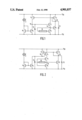
FIG. 1 shows a first embodiment of an oscillator circuit in accordance with the invention, and
FIG. 2 shows a second embodiment of an oscillator circuit in accordance with the invention.
DESCRIPTION OF THE PREFERRED EMBODIMENTS
Referring to FIG. 1, amplifier comprises the series connection of transistors N1 and P1 between power supply terminals VDD and VSS. Between the junction point K1 of these transistors and the control terminal of the transistor N1 there is connected the feedback network, for example in the form of a semiconductor delay line DL. The length and the process variables, such as the sheet resistance and the sheet capacitance, of this delay line DL determined the oscillator frequency. An amplitude detector, formed by the series connection of transistors N2 and P2, has an input connect to the junction point K1. The output of the amplitude detector, being the junction point K2, is connected to the control electrode of a transistor P3 which is connected in series with a transistor N3. The control terminal of the latter transistor receives a reference voltage associated with a conducted current equal or proportional to Iref. The transistor P3 and the transistor N3 thus form current sources. Their junction point K3 is connected to the control terminal of the transistor P1. Buffer capacitances C2 and C3 are connected to the junction points K2 and K3, respectively. Because of their integrating effect, these capacitances slightly reduce the control sensitivity.
The operation is as follows. At the start, the transistors N2, P2 and P3 are blocked. The reference current then forces the transistor N3 to reduce the control voltage at the junction point K3, so that the transistor P1 becomes highly conductive. Oscillation starts as soon as the current conducted by P1 is sufficiently large to satisfy the oscillation fluctuation into a current which is integrated on the capacitance C2. The voltage across C2 then decreases, with the result that the transistor P3 becomes conductive. The potential at the junction point K3 then increases, so that the current passage through the transistor P1 is adjusted to a lower value.
FIG. 2 shows a second embodiment of the oscillator circuit in accordance with the invention. The oscillator consists of, for example the amplifier N1 /P1 which is fed back via the delay line DL. The amplitude detector N2 /P2 connected to the output thereof controls the current source P3 which is connected in series with the reference current source N3. The amplifier N1 /P1 is fed via the transistor P4, a control electrode of which is connected to the junction point K3 between the current sources P3 and N3. As will be obvious to those skilled in the art, the transistor P4 is provided in order to achieve quick starting.

Claims (5)

What is claimed is:
1. An oscillator circuit comprising:
an amplifier controlled by means of a control voltage on a control terminal and which comprises a feedback circuit coupled between an amplifier input and an amplifier output;
an amplitude controller which comprises an amplitude detector for controlling the oscillation amplitude in dependence on a detected amplitude and a first and a second current source for supplying currents of mutually opposed polarity to the control terminal, at least one of the current sources being controllable by the amplitude controller in dependence on an amplitude which is detected during at the most one half of an oscillation period.
2. An oscillator circuit as claimed in claim 1, wherein the amplifier comprises a series connection of current paths of a first transistor and a second transistor of a first and a second conductivity type, respectively, and in which the feedback circuit is connected between a control electrode of the first transistor and a junction point of the current paths, wherein the amplitude detector comprises a series connection of current paths of a third transistor and a fourth transistor of the first and the second conductivity type, respectively, a control electrode of the third transistor being connected to the feedback circuit, a control electrode of the fourth transistor being connected to a first junction point between the third and the fourth transistor, the current sources comprising a series connection of current paths of a fifth transistor and a sixth transistor of the first and the second conductivity type, respectively, a control electrode of the sixth transistor being connected to the first junction point, the fifth transistor conducting a reference current, a second junction point between the current paths of the fifth and the sixth transistor being connected to the control electrode of the second transistor.
3. An oscillator circuit as claimed in claim 1 wherein the amplifier comprises a connection of current paths of a first transistor and a second transistor of a first and a second conductivity type, respectively, and in which the feedback circuit is connected between a control electrode of the first transistor and the junction point of the current paths, wherein the amplitude detector comprises a series connection of current paths of a third transistor and a fourth transistor of the first and the second conductivity type, respectively, a control electrode of the third transistor being connected to the feedback circuit, a control electrode of the fourth transistor being connected to a first junction point between the third and the fourth transistor, the current sources comprising a series connection of a fifth transistor and a sixth transistor of the first and the second conductivity type, respectively, a control electrode of the sixth transistor being connected to the first junction point, the fifth transistor conducting a reference current, a second junction point between the fifth and the sixth transistor being connected to a control electrode of a seventh transistor of the second second junction point between the fifth and the sixth transistor being connected to a control electrode of a seventh transistor of the second conductivity type, a current path of said seventh transistor being connected between one terminal of a power supply and the current path of the second transistor.
4. An oscillator circuit as claimed in claim 3, further comprising at least one of the following buffer capacitances: a first buffer capacitance coupled between the frist junction point and one of two power supply terminals; a second buffer capacitance coupled between the second junction point and one of two power supply terminals.
5. An oscillator circuit as claimed in claim 2, further comprising at least one of the following buffer capacitances: a first buffer capacitance coupled between the first junction point and one of two power supply terminals; a second buffer capacitance coupled between the second junction point and one of two power supply terminals.
US07/239,574 1987-09-08 1988-09-01 Oscillator with amplitude stabilizing circuit Expired - Lifetime US4901037A (en)

Applications Claiming Priority (2)

Application Number Priority Date Filing Date Title
NL8702122 1987-09-08
NL8702122A NL8702122A (en) 1987-09-08 1987-09-08 OSCILLATOR CIRCUIT WITH AMPLITUDER CONTROLLER.

Publications (1)

Publication Number Publication Date
US4901037A true US4901037A (en) 1990-02-13

Family

ID=19850572

Family Applications (1)

Application Number Title Priority Date Filing Date
US07/239,574 Expired - Lifetime US4901037A (en) 1987-09-08 1988-09-01 Oscillator with amplitude stabilizing circuit

Country Status (6)

Country Link
US (1) US4901037A (en)
EP (1) EP0307988B1 (en)
JP (1) JP3004019B2 (en)
KR (1) KR970004438B1 (en)
DE (1) DE3879832T2 (en)
NL (1) NL8702122A (en)

Cited By (3)

* Cited by examiner, † Cited by third party
Publication number Priority date Publication date Assignee Title
WO1991015071A1 (en) * 1990-03-19 1991-10-03 Albert John Mallinckrodt Integrated cellular communications system
WO1998006170A1 (en) * 1996-08-07 1998-02-12 Philips Electronics N.V. Oscillator
US20070046385A1 (en) * 2005-08-29 2007-03-01 Micron Technology, Inc. Time delay oscillator for integrated circuits

Citations (3)

* Cited by examiner, † Cited by third party
Publication number Priority date Publication date Assignee Title
US4433371A (en) * 1980-10-16 1984-02-21 Ebauches, Electroniques, S.A. Converter for converting an a.c. voltage into a direct current and an oscillator circuit using said converter
US4560958A (en) * 1984-02-24 1985-12-24 Tektronix, Inc. State variable oscillator having improved rejection of leveler-induced distortion
US4608544A (en) * 1983-11-29 1986-08-26 U.S. Philips Corporation Oscillator circuit

Family Cites Families (1)

* Cited by examiner, † Cited by third party
Publication number Priority date Publication date Assignee Title
DE3223338A1 (en) * 1982-06-23 1984-01-05 Eurosil GmbH, 8057 Eching Integrated field effect transistor oscillator circuit

Patent Citations (3)

* Cited by examiner, † Cited by third party
Publication number Priority date Publication date Assignee Title
US4433371A (en) * 1980-10-16 1984-02-21 Ebauches, Electroniques, S.A. Converter for converting an a.c. voltage into a direct current and an oscillator circuit using said converter
US4608544A (en) * 1983-11-29 1986-08-26 U.S. Philips Corporation Oscillator circuit
US4560958A (en) * 1984-02-24 1985-12-24 Tektronix, Inc. State variable oscillator having improved rejection of leveler-induced distortion

Cited By (6)

* Cited by examiner, † Cited by third party
Publication number Priority date Publication date Assignee Title
WO1991015071A1 (en) * 1990-03-19 1991-10-03 Albert John Mallinckrodt Integrated cellular communications system
WO1998006170A1 (en) * 1996-08-07 1998-02-12 Philips Electronics N.V. Oscillator
US20070046385A1 (en) * 2005-08-29 2007-03-01 Micron Technology, Inc. Time delay oscillator for integrated circuits
US7295081B2 (en) * 2005-08-29 2007-11-13 Micron Technology, Inc. Time delay oscillator for integrated circuits
US20080007359A1 (en) * 2005-08-29 2008-01-10 Micron Technology, Inc. Time delay oscillator for integrated circuits
US7629858B2 (en) * 2005-08-29 2009-12-08 Micron Technology, Inc. Time delay oscillator for integrated circuits

Also Published As

Publication number Publication date
KR970004438B1 (en) 1997-03-27
DE3879832T2 (en) 1993-09-30
KR890005967A (en) 1989-05-18
JP3004019B2 (en) 2000-01-31
DE3879832D1 (en) 1993-05-06
EP0307988A1 (en) 1989-03-22
EP0307988B1 (en) 1993-03-31
JPS6472603A (en) 1989-03-17
NL8702122A (en) 1989-04-03

Similar Documents

Publication Publication Date Title
US6005378A (en) Compact low dropout voltage regulator using enhancement and depletion mode MOS transistors
US5982227A (en) CMOS current source circuit
JP2592234B2 (en) Semiconductor device
EP0766164A2 (en) Voltage regulator with load pole stabilization
JPH0951266A (en) Circuit and method for maintaining substrate voltage to desired value
US4893095A (en) Frequency stabilized oscillator
EP0967538B1 (en) Output control circuit for a voltage regulator
US5365161A (en) Stabilized voltage supply
US4437023A (en) Current mirror source circuitry
US4158804A (en) MOSFET Reference voltage circuit
US4578633A (en) Constant current source circuit
US5216291A (en) Buffer circuit having high stability and low quiescent current consumption
US4532467A (en) CMOS Circuits with parameter adapted voltage regulator
JPH06138965A (en) Reference-voltage generating circuit for integrated circuit
US7049833B2 (en) Method for optimizing the accuracy of an electronic circuit
US4556805A (en) Comparator circuit having hysteresis voltage substantially independent of variation in power supply voltage
JP2590378B2 (en) Logic circuit
US4901037A (en) Oscillator with amplitude stabilizing circuit
US4808909A (en) Bias voltage and constant current supply circuit
US5120994A (en) Bicmos voltage generator
KR940027322A (en) Semiconductor integrated circuit device
US6414516B1 (en) CMOS output amplifier independent of temperature, supply voltage and manufacturing quality of transistors
US4996499A (en) Amplitude stabilized oscillator amplifier
JP2953226B2 (en) Reference voltage generation circuit
US3984761A (en) Line powered voltage regulator

Legal Events

Date Code Title Description
AS Assignment

Owner name: U.S. PHILIPS CORPORATION, 100 EAST 42ND ST., NEW Y

Free format text: ASSIGNMENT OF ASSIGNORS INTEREST.;ASSIGNOR:FELLER, ERNST;REEL/FRAME:005148/0387

Effective date: 19890908

STCF Information on status: patent grant

Free format text: PATENTED CASE

FEPP Fee payment procedure

Free format text: PAYOR NUMBER ASSIGNED (ORIGINAL EVENT CODE: ASPN); ENTITY STATUS OF PATENT OWNER: LARGE ENTITY

FPAY Fee payment

Year of fee payment: 4

FPAY Fee payment

Year of fee payment: 8

FPAY Fee payment

Year of fee payment: 12

AS Assignment

Owner name: NXP B.V., NETHERLANDS

Free format text: ASSIGNMENT OF ASSIGNORS INTEREST;ASSIGNOR:U.S. PHILIPS CORPORATION;REEL/FRAME:021523/0086

Effective date: 20080623