EP0473192A2 - A circuit for reducing resonance voltage - Google Patents
A circuit for reducing resonance voltage Download PDFInfo
- Publication number
- EP0473192A2 EP0473192A2 EP91114659A EP91114659A EP0473192A2 EP 0473192 A2 EP0473192 A2 EP 0473192A2 EP 91114659 A EP91114659 A EP 91114659A EP 91114659 A EP91114659 A EP 91114659A EP 0473192 A2 EP0473192 A2 EP 0473192A2
- Authority
- EP
- European Patent Office
- Prior art keywords
- voltage
- cable
- circuit
- diodes
- power supply
- Prior art date
- Legal status (The legal status is an assumption and is not a legal conclusion. Google has not performed a legal analysis and makes no representation as to the accuracy of the status listed.)
- Granted
Links
Images

Classifications
-
- H—ELECTRICITY
- H02—GENERATION; CONVERSION OR DISTRIBUTION OF ELECTRIC POWER
- H02M—APPARATUS FOR CONVERSION BETWEEN AC AND AC, BETWEEN AC AND DC, OR BETWEEN DC AND DC, AND FOR USE WITH MAINS OR SIMILAR POWER SUPPLY SYSTEMS; CONVERSION OF DC OR AC INPUT POWER INTO SURGE OUTPUT POWER; CONTROL OR REGULATION THEREOF
- H02M7/00—Conversion of AC power input into DC power output; Conversion of DC power input into AC power output
- H02M7/42—Conversion of DC power input into AC power output without possibility of reversal
- H02M7/44—Conversion of DC power input into AC power output without possibility of reversal by static converters
- H02M7/48—Conversion of DC power input into AC power output without possibility of reversal by static converters using discharge tubes with control electrode or semiconductor devices with control electrode
-
- H—ELECTRICITY
- H02—GENERATION; CONVERSION OR DISTRIBUTION OF ELECTRIC POWER
- H02M—APPARATUS FOR CONVERSION BETWEEN AC AND AC, BETWEEN AC AND DC, OR BETWEEN DC AND DC, AND FOR USE WITH MAINS OR SIMILAR POWER SUPPLY SYSTEMS; CONVERSION OF DC OR AC INPUT POWER INTO SURGE OUTPUT POWER; CONTROL OR REGULATION THEREOF
- H02M7/00—Conversion of AC power input into DC power output; Conversion of DC power input into AC power output
-
- H—ELECTRICITY
- H02—GENERATION; CONVERSION OR DISTRIBUTION OF ELECTRIC POWER
- H02M—APPARATUS FOR CONVERSION BETWEEN AC AND AC, BETWEEN AC AND DC, OR BETWEEN DC AND DC, AND FOR USE WITH MAINS OR SIMILAR POWER SUPPLY SYSTEMS; CONVERSION OF DC OR AC INPUT POWER INTO SURGE OUTPUT POWER; CONTROL OR REGULATION THEREOF
- H02M1/00—Details of apparatus for conversion
- H02M1/12—Arrangements for reducing harmonics from AC input or output
Definitions
- the present invention relates to an inverter unit for suppressing the occurrence of a resonance voltage in a long AC power cable.
- a resonance voltage is generated by an inductance Lo and a capacitance Co of a cable connecting the output of a voltage source inverter (hereinafter referred to as the "inverter unit") and a motor as a load.
- the output voltage of the inverter unit changes in stepwise fashion, generating a voltage oscillation having twice the amplitude of the output voltage in the worst case.
- FIG. 5 provides an example of a conventional inverter unit circuit, wherein an electrolytic capacitor 10 operates as a DC power supply connected to a motor 40 by cable 30.
- An inverter circuit 20 converts a supplied DC voltage to a square-wave AC voltage for output to the motor 40 which is the load.
- the inverter unit is constituted by the DC power supply 10 and inverter circuit 20.
- the inverter unit could be equipped with a converter circuit (not illustrated) for converting the AC voltage of a commercial power supply provided by an AC power supply and outputting a DC voltage.
- the DC voltage could be smoothed by the electrolytic capacitor 10 and supplied to the inverter circuit 20.
- the converter circuit and capacitor 10 would constitute the DC power supply.
- the DC voltage supplied by the electrolytic capacitor 10 is converted by switching transistors 21, 22 into a square-wave AC voltage, which then is transmitted to motor 40 via cable 30 to control the rotation of the motor 40.
- the cable 30 connecting the inverter circuit 20 and motor 40 may be rather long. In such a case, the inductance Lo and capacitance Co of the cable 30 cannot be considered negligible.
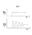
- Figure 6 shows an equivalent circuit of the cable 30, and Figure 7 illustrates the waveforms of the input voltage Vi and output voltage Vo (terminal voltage to the motor 40) of the cable 30.
- the carrier frequency is increased 10 or more times, the number of times that the oscillating voltage is applied to the motor 40 naturally increases, causing further deterioration of the motor 40.
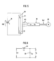
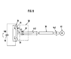
- some conventional circuits have employed reactors 51 of sufficiently large inductance L2 inserted as oscillation suppression means 50, as shown in Figure 8, between each output end of the inverter circuit 20 and each input end of the cable 30.
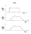
- Vi 1 , Vi 2 , and Vo 2 in Figure 9 illustrate the stepwise input voltage Vi and output voltage Vi 2 (input voltage of the cable 30) of said inductance L 2 , and the motor terminal voltage Vo 2 (output voltage of the cable 30).
- the reactors 51 smooth the leading and trailing edges of the fast-rising voltage Vi 1 as indicated by the voltage Vi 2 , to suppress the oscillation in the cable 30.
- the known inverter unit is disadvantageous in that an increase in cable length will cause a large oscillating voltage to be applied to the motor end, thus deteriorating the insulation of the motor.
- reactors may be inserted between the cable and the inverter circuit output end.
- reactors having a relatively large inductance are required to make the leading edge of the voltage smooth enough to provide an oscillation suppressing effect, but the reactors will adversely affect motor control performance due to their voltage drop.
- relatively large-sized reactors are required because of their large inductances, posing problems of increased size and cost.
- an object of the present invention to overcome the disadvantages in the prior art by providing an inverter unit which prevents a large oscillating voltage from being applied to a load if the wiring length of a cable is increased.
- An inverter unit of a first embodiment of the invention includes an inverter circuit for switching and converting a DC voltage supplied by a DC power supply into an AC voltage, and voltage clamping means for suppressing the rise of a voltage supplied to a load due to voltage resonance in a cable for supplying an AC output from the inverter to the load.
- the voltage clamping circuit may include reactors inserted between the inverter circuit and the cable, and a pair of clamping series structures for clamping the resonance voltage of the reactors and the cable.
- An inverter unit of a second embodiment of the invention includes an inverter circuit for switching and converting a DC voltage supplied by a DC power supply into an AC voltage, and a voltage clamping circuit for suppressing the rise of a voltage supplied to a load due to voltage resonance in a cable for supplying an AC output from the inverter to the load.
- the voltage clamping means may include reactors inserted between the inverter circuit and the cable, pairs of diodes for clamping the resonance voltage of the reactors and the cable, and a capacitor inserted between the pairs of diodes for absorbing the first wave of the resonance voltage.
- the first reactors in the first embodiment are inserted between the inverter circuit and cable; one end of the pair of clamping series structures is connected to the cable and the other end is connected with the DC power supply to clamp the crest value of the resonance voltage of the first reactors and the cable to approximately the DC power voltage, thereby suppressing the rise of the voltage supplied to the load.
- the reactors in the second embodiment are inserted between the inverter circuit and the cable, one end of the pair of diodes is connected with the reactors and the other end is connected with the DC power supply via the resistors to clamp the crest value of the resonance voltage of the reactors and the cable to approximately the DC power voltage.
- the capacitor is inserted between the pairs of diodes to absorb the first wave of the resonance voltage, thus suppressing the rise of the voltage supplied to the load.
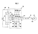
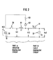
- Figure 1 is a wiring diagram of the inverter unit and Figure 2 is an equivalent circuit diagram of the unit shown in Figure 1.
- voltage clamping circuit 60 comprising reactors 61 A-61 C is shown inserted between the inverter circuit 20 and the cable 30.
- a first set of series circuits consisting of diodes 62A-62C and resistors 63A-63C are shown with diodes 62A-62C connected to the output of the reactors 61A-61C and the cable 30.
- a second set of series circuits consisting of diodes 64A-64C and resistors 65A-65C are similarly connected to the output of reactors 61A-61C, with the diodes 64A-64C serving as the connecting points.
- the resistors of the first and second sets of series circuits are respectively connected with the positive and negative poles of the DC power supply in the form of an electrolytic capacitor 10.lndividual circuits of the first set of series circuits consisting of the diodes 62A-62C and resistors 63A-63C and individual circuits of the second set of series circuits constituting the diodes 64A-64C and resistors 65A-65C constitute a pair of clamping series structures for clamping the resonance voltage of the reactors 61 A-61 C and the cable 30.
- the inductances L, of the reactors 61 A-61 C should be selected to be sufficiently large compared to the wiring inductance L o of the cable 30.
- the output ends of the reactors 61A-61C are connected to the electrolytic capacitor 10 via the clamping series structures comprising the diodes 62A-62C and resistors 63A-63C.
- the diodes 62A-62C are switched on, clamping Vi 2 to V DC .
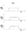
- Figure 3 illustrates relationships between the output voltage Vi 1 of the inverter circuit 20, the output voltage Vi 2 of the reactors 61A-61C, the output voltage (motor input voltage) Vo 2 of the cable 30, and elapsed time t.
- resistors 63A-63C, 65A-65C limit the current flowing in the diodes at the time of voltage clamping in Figure 1, those of appropriate resistance values should be selected in accordance with the current resistance of the diodes 62A-62C, 64A-64C.
- the resistors 63A-63C, 65A-65C and the second reactors need not be inserted at all.
- Figure 4 provides an example of an inverter unit circuit according to a second embodiment of the invention. This unit is similar to that shown in Figure 1 but adds resistors 66, 67 and a capacitor 68. In the first embodiment shown in Figure 1, a large value R 1 must be selected for the resistors 63A-63C, 65A-65C, leading to a potential reduction in voltage effect.
- the capacitor 68 of capacitance C 1 smaller than the capacitance Co of the cable 30 is inserted and connected in parallel to the pairs of diodes 62A-62C, 64A-64C to cause the first wave having the largest oscillation to be clamped by the capacitor 68 and the following waves to be absorbed by the electrolytic capacitor 10 via the resistors 66, 67.
- This circuit allows the use of diodes which are relatively small in surge resistance and current resistance.
- the circuit illustrated in Figure 4 causes surges from the diodes 62A-62C, 64A-64C to be clamped by the capacitor 68 without passing through the resistors 66, 67 so that external noise coming from the cable 30 may be absorbed. Further, the circuit is advantageous in that little heat is generated by the resistors 66, 67.
Landscapes
- Engineering & Computer Science (AREA)
- Power Engineering (AREA)
- Inverter Devices (AREA)
- Protection Of Static Devices (AREA)
- Power Conversion In General (AREA)
- Emergency Protection Circuit Devices (AREA)
Abstract
Description
- The present invention relates to an inverter unit for suppressing the occurrence of a resonance voltage in a long AC power cable.
- A resonance voltage is generated by an inductance Lo and a capacitance Co of a cable connecting the output of a voltage source inverter (hereinafter referred to as the "inverter unit") and a motor as a load. The output voltage of the inverter unit changes in stepwise fashion, generating a voltage oscillation having twice the amplitude of the output voltage in the worst case.
- Figure 5 provides an example of a conventional inverter unit circuit, wherein an
electrolytic capacitor 10 operates as a DC power supply connected to amotor 40 bycable 30. Aninverter circuit 20 converts a supplied DC voltage to a square-wave AC voltage for output to themotor 40 which is the load. The inverter unit is constituted by theDC power supply 10 andinverter circuit 20. In practice, the inverter unit could be equipped with a converter circuit (not illustrated) for converting the AC voltage of a commercial power supply provided by an AC power supply and outputting a DC voltage. The DC voltage could be smoothed by theelectrolytic capacitor 10 and supplied to theinverter circuit 20. The converter circuit andcapacitor 10 would constitute the DC power supply. - In operation, the DC voltage supplied by the
electrolytic capacitor 10 is converted byswitching transistors motor 40 viacable 30 to control the rotation of themotor 40. - In common practice, however, the
cable 30 connecting theinverter circuit 20 andmotor 40 may be rather long. In such a case, the inductance Lo and capacitance Co of thecable 30 cannot be considered negligible. - Figure 6 shows an equivalent circuit of the
cable 30, and Figure 7 illustrates the waveforms of the input voltage Vi and output voltage Vo (terminal voltage to the motor 40) of thecable 30. - By entering the step voltage Vi as shown in Figure 7 into the input port of the equivalent circuit shown in Figure 6, the terminal voltage Vo of the
motor 40 oscillates as shown in Figure 7. This oscillating voltage becomes twice the input voltage (output voltage of the inverter circuit 20) of thecable 30 in the worst case, causing premature deterioration of the insulation of themotor 40. - In general, when a step-shaped DC voltage E is applied at time t = 0 to a circuit where inductance L and capacitance C are connected in series, a relationship between a voltage Eout generated at the capacitance C and elapsed time t is expressed as follows:

- Hence, if

- in expression (1), Eout is maximum; Eout = 2E, i.e. the output voltage reaches twice the input voltage.
- Recently, low-noise inverters have been put on the market which have been enhanced in carrier frequency from the previous 1-2kHz to 10kHz or higher by employing power MOSFETs and IGBTs as power elements that are higher in switching speed than the
transistors inverter circuit 20. Because of their large ratios of voltage change, however, such high-speed switching elements are liable to increase the crest value of the oscillating voltage of terminal voltage Vo of themotor 40. - In addition, if the carrier frequency is increased 10 or more times, the number of times that the oscillating voltage is applied to the
motor 40 naturally increases, causing further deterioration of themotor 40. - In order to suppress the oscillating voltage, some conventional circuits have employed
reactors 51 of sufficiently large inductance L2 inserted as oscillation suppression means 50, as shown in Figure 8, between each output end of theinverter circuit 20 and each input end of thecable 30. Vi1, Vi2, and Vo2 in Figure 9 illustrate the stepwise input voltage Vi and output voltage Vi2 (input voltage of the cable 30) of said inductance L2, and the motor terminal voltage Vo2 (output voltage of the cable 30). As shown in Figure 9, thereactors 51 smooth the leading and trailing edges of the fast-rising voltage Vi1 as indicated by the voltage Vi2, to suppress the oscillation in thecable 30. - In the configuration as described above, the known inverter unit is disadvantageous in that an increase in cable length will cause a large oscillating voltage to be applied to the motor end, thus deteriorating the insulation of the motor. To prevent this, reactors may be inserted between the cable and the inverter circuit output end. In this case, reactors having a relatively large inductance are required to make the leading edge of the voltage smooth enough to provide an oscillation suppressing effect, but the reactors will adversely affect motor control performance due to their voltage drop. In addition, relatively large-sized reactors are required because of their large inductances, posing problems of increased size and cost.
- Accordingly, it is an object of the present invention to overcome the disadvantages in the prior art by providing an inverter unit which prevents a large oscillating voltage from being applied to a load if the wiring length of a cable is increased.
- An inverter unit of a first embodiment of the invention includes an inverter circuit for switching and converting a DC voltage supplied by a DC power supply into an AC voltage, and voltage clamping means for suppressing the rise of a voltage supplied to a load due to voltage resonance in a cable for supplying an AC output from the inverter to the load. The voltage clamping circuit may include reactors inserted between the inverter circuit and the cable, and a pair of clamping series structures for clamping the resonance voltage of the reactors and the cable.
- An inverter unit of a second embodiment of the invention includes an inverter circuit for switching and converting a DC voltage supplied by a DC power supply into an AC voltage, and a voltage clamping circuit for suppressing the rise of a voltage supplied to a load due to voltage resonance in a cable for supplying an AC output from the inverter to the load. The voltage clamping means may include reactors inserted between the inverter circuit and the cable, pairs of diodes for clamping the resonance voltage of the reactors and the cable, and a capacitor inserted between the pairs of diodes for absorbing the first wave of the resonance voltage.
- The first reactors in the first embodiment are inserted between the inverter circuit and cable; one end of the pair of clamping series structures is connected to the cable and the other end is connected with the DC power supply to clamp the crest value of the resonance voltage of the first reactors and the cable to approximately the DC power voltage, thereby suppressing the rise of the voltage supplied to the load.
- The reactors in the second embodiment are inserted between the inverter circuit and the cable, one end of the pair of diodes is connected with the reactors and the other end is connected with the DC power supply via the resistors to clamp the crest value of the resonance voltage of the reactors and the cable to approximately the DC power voltage. The capacitor is inserted between the pairs of diodes to absorb the first wave of the resonance voltage, thus suppressing the rise of the voltage supplied to the load.
-
- Figure 1 is a circuit diagram illustrating an inverter unit, a cable, and a motor according to a first embodiment of the invention.
- Figure 2 is an equivalent circuit diagram of the inverter unit and cable portions shown in Figure 1.
- Figure 3 illustrates the voltage waveform of each portion versus time elapsed in the equivalent circuit shown in Figure 2.
- Figure 4 shows an inverter unit according to a second embodiment of the invention.
- Figure 5 is the circuit diagram of a conventional inverter unit.
- Figure 6 is the equivalent circuit of a cable.
- Figure 7 illustrates input and output voltage waveforms versus time elapsed in the cable shown in Figure 6.
- Figure 8 is the circuit diagram of another conventional inverter unit.
- Figure 9 illustrates the voltage waveform of each portion versus time elapsed in the circuit diagram shown in Figure 8.
- One embodiment of the invention will now be described in reference to Figures 1 to 3. In the drawings, like reference characters designate like or corresponding parts throughout the different views.
- Figure 1 is a wiring diagram of the inverter unit and Figure 2 is an equivalent circuit diagram of the unit shown in Figure 1. Referring to Figures 1 and 2,
voltage clamping circuit 60 comprisingreactors 61 A-61 C is shown inserted between theinverter circuit 20 and thecable 30. A first set of series circuits consisting ofdiodes 62A-62C andresistors 63A-63C are shown withdiodes 62A-62C connected to the output of thereactors 61A-61C and thecable 30. A second set of series circuits consisting ofdiodes 64A-64C andresistors 65A-65C are similarly connected to the output ofreactors 61A-61C, with thediodes 64A-64C serving as the connecting points. The resistors of the first and second sets of series circuits are respectively connected with the positive and negative poles of the DC power supply in the form of an electrolytic capacitor 10.lndividual circuits of the first set of series circuits consisting of thediodes 62A-62C andresistors 63A-63C and individual circuits of the second set of series circuits constituting thediodes 64A-64C andresistors 65A-65C constitute a pair of clamping series structures for clamping the resonance voltage of thereactors 61 A-61 C and thecable 30. - The inductances L, of the
reactors 61 A-61 C should be selected to be sufficiently large compared to the wiring inductance Lo of thecable 30. - Figure 2 shows an equivalent circuit of the circuit portion made up of the
electrolytic capacitor 10,inverter circuit 20,voltage clamping circuit 60, andcable 30 as shown in Figure 1. Since the inductances have been selected to satisfy L1 » Lo as described above, thecable 30 input voltage (output voltage of the reactors 61) Vi2 and output voltage (motor input voltage) Vo2 are approximately equal, i.e. Vi2≃Vo2. By turning on a switch in the equivalent circuit of theinverter circuit 20, the resonance voltage Vi2 (=Vo2) is generated by the inductances L1 of thereactors 61 and the capacitance Co of thecable 30. However, the input ends of thecable 30, i.e. the output ends of thereactors 61A-61C, are connected to theelectrolytic capacitor 10 via the clamping series structures comprising thediodes 62A-62C andresistors 63A-63C. Hence, when the oscillating voltage Vi rises above the terminal voltage VDC of theelectrolytic capacitor 10, thediodes 62A-62C are switched on, clamping Vi2 to VDC. - Figure 3 illustrates relationships between the output voltage Vi1 of the
inverter circuit 20, the output voltage Vi2 of thereactors 61A-61C, the output voltage (motor input voltage) Vo2 of thecable 30, and elapsed time t. Here Vi2≃Vo2 and, as a result, a larger voltage than VDC is not applied as the motor input voltage Vo2. - In Figure 2, the impedance of the
motor 40 is not indicated because it is sufficiently larger than that of thecable 30 and will not be needed to understand the circuit operation. - Since the
resistors 63A-63C, 65A-65C limit the current flowing in the diodes at the time of voltage clamping in Figure 1, those of appropriate resistance values should be selected in accordance with the current resistance of thediodes 62A-62C, 64A-64C. - In Figure 1, a similar effect may be produced when additional reactors (not illustrated) are inserted instead of the
resistors 63A-63C, 65A-65C to constitute the clamping series structures together with thediodes 62A-62C, 64A-64C. A similar effect may also be produced by inserting varistors instead ofdiodes 62A-62C, 64A-64C. - Moreover, when the current resistance of the
diodes 62A-62C, 64A-64C is sufficiently large, theresistors 63A-63C, 65A-65C and the second reactors (not illustrated) need not be inserted at all. - Figure 4 provides an example of an inverter unit circuit according to a second embodiment of the invention. This unit is similar to that shown in Figure 1 but adds
resistors capacitor 68. In the first embodiment shown in Figure 1, a large value R1 must be selected for theresistors 63A-63C, 65A-65C, leading to a potential reduction in voltage effect. In the circuit configuration in Figure 4, however, thecapacitor 68 of capacitance C1 smaller than the capacitance Co of thecable 30 is inserted and connected in parallel to the pairs ofdiodes 62A-62C, 64A-64C to cause the first wave having the largest oscillation to be clamped by thecapacitor 68 and the following waves to be absorbed by theelectrolytic capacitor 10 via theresistors - Unlike the circuit shown in Figure 1, the circuit illustrated in Figure 4 causes surges from the
diodes 62A-62C, 64A-64C to be clamped by thecapacitor 68 without passing through theresistors cable 30 may be absorbed. Further, the circuit is advantageous in that little heat is generated by theresistors - In Figure 4, a similar effect may be produced when reactors (not illustrated) are inserted instead of the
resistors 63A-63C, 65A-65C to constitute the clamping series structures together with thediodes 62A-62C, 64A-64C. A similar effect may also be produced by inserting varistors instead ofdiodes 62A-62C, 64A-64C. - It will be apparent that the invention, as described above, achieves a relatively compact and low-cost inverter unit which suppresses the rise of the voltage supplied to the load due to voltage resonance in the cable.
Claims (8)
Applications Claiming Priority (3)
| Application Number | Priority Date | Filing Date | Title |
|---|---|---|---|
| JP229239/90 | 1990-08-30 | ||
| JP2229239A JP2707814B2 (en) | 1990-08-30 | 1990-08-30 | Inverter device |
| JP22923990 | 1990-08-30 |
Publications (4)
| Publication Number | Publication Date |
|---|---|
| EP0473192A2 true EP0473192A2 (en) | 1992-03-04 |
| EP0473192A3 EP0473192A3 (en) | 1992-06-17 |
| EP0473192B1 EP0473192B1 (en) | 1995-07-19 |
| EP0473192B2 EP0473192B2 (en) | 1999-09-01 |
Family
ID=16889005
Family Applications (1)
| Application Number | Title | Priority Date | Filing Date |
|---|---|---|---|
| EP91114659A Expired - Lifetime EP0473192B2 (en) | 1990-08-30 | 1991-08-30 | A circuit for reducing resonance voltage |
Country Status (5)
| Country | Link |
|---|---|
| EP (1) | EP0473192B2 (en) |
| JP (1) | JP2707814B2 (en) |
| KR (1) | KR960010827B1 (en) |
| DE (1) | DE69111338T3 (en) |
| HK (1) | HK1006050A1 (en) |
Cited By (12)
| Publication number | Priority date | Publication date | Assignee | Title |
|---|---|---|---|---|
| DE9307806U1 (en) * | 1993-05-24 | 1993-08-26 | Siemens Ag | Inverter output filter |
| EP0682402A1 (en) * | 1994-05-11 | 1995-11-15 | Schaffner Elektronik Ag | Output magnitudes rise limiting device for self-commutated constant voltage intermediate circuit converter |
| WO1998001937A3 (en) * | 1996-07-08 | 1998-02-26 | Paavo Eero Paloniemi | A connection means between a frequency converter and its load |
| DE19736786A1 (en) * | 1997-08-23 | 1999-02-25 | Asea Brown Boveri | U-converter |
| WO2001039347A1 (en) * | 1999-11-26 | 2001-05-31 | Siemens Aktiengesellschaft | Protective device against overpotential in the terminals of electrical equipment, caused by switching operations |
| WO2002023705A1 (en) * | 2000-09-12 | 2002-03-21 | Bombardier Transportation Gmbh | Filter circuit configuration for a converter circuit |
| DE102006036092A1 (en) * | 2006-08-02 | 2008-02-07 | Siemens Ag | sine filter |
| DE102005045552B4 (en) * | 2005-09-23 | 2008-04-17 | Siemens Ag | circuitry |
| DE102007039764B3 (en) * | 2007-08-22 | 2008-12-24 | Dräger Medical AG & Co. KG | Ventilator for respiration device, has control unit connected to three stator coils, and has switch unit connected in series, where partial switches of each switch unit is provided for activating stator coil |
| AT502355B1 (en) * | 2005-09-08 | 2009-07-15 | Elin Ebg Traction Gmbh | POWER SUPPLY FOR AN ELECTRICAL MACHINE |
| EP3255767A1 (en) * | 2016-06-07 | 2017-12-13 | ABB Technology Oy | Output filter for inverter leg |
| EP4143956A4 (en) * | 2020-04-29 | 2024-06-05 | BAE Systems Controls Inc. | Ac drive dv/dt filter using reverse recovery charge of diodes |
Families Citing this family (5)
| Publication number | Priority date | Publication date | Assignee | Title |
|---|---|---|---|---|
| JP4557616B2 (en) * | 2004-07-02 | 2010-10-06 | 株式会社日立産機システム | Power converter |
| JP4558089B2 (en) * | 2009-10-19 | 2010-10-06 | 株式会社日立産機システム | Motor and motor drive system |
| JP6508505B2 (en) * | 2013-12-19 | 2019-05-08 | パナソニックIpマネジメント株式会社 | Inverter circuit |
| JP7127290B2 (en) * | 2018-02-08 | 2022-08-30 | 富士電機株式会社 | Surge voltage suppressor, power conversion device and polyphase motor drive device using the same |
| JP7135494B2 (en) * | 2018-06-26 | 2022-09-13 | 富士電機株式会社 | MOTOR OVERVOLTAGE PROTECTION DEVICE, POWER CONVERSION DEVICE USING THE SAME, AND MULTI-PHASE MOTOR DRIVE DEVICE |
Family Cites Families (3)
| Publication number | Priority date | Publication date | Assignee | Title |
|---|---|---|---|---|
| US3568021A (en) * | 1969-05-15 | 1971-03-02 | Gen Electric | Low cost variable input voltage inverter with reliable commutation |
| US3668507A (en) * | 1971-06-04 | 1972-06-06 | Dmitry Evgenievich Kadomsky | Apparatus for damping oscillations in three-phase bridge converters |
| JPH0757067B2 (en) * | 1986-08-08 | 1995-06-14 | 株式会社明電舎 | Surge voltage suppression circuit |
-
1990
- 1990-08-30 JP JP2229239A patent/JP2707814B2/en not_active Expired - Lifetime
-
1991
- 1991-08-26 KR KR1019910014770A patent/KR960010827B1/en not_active Expired - Fee Related
- 1991-08-30 DE DE69111338T patent/DE69111338T3/en not_active Expired - Lifetime
- 1991-08-30 EP EP91114659A patent/EP0473192B2/en not_active Expired - Lifetime
-
1998
- 1998-06-11 HK HK98105197A patent/HK1006050A1/en not_active IP Right Cessation
Cited By (13)
| Publication number | Priority date | Publication date | Assignee | Title |
|---|---|---|---|---|
| DE9307806U1 (en) * | 1993-05-24 | 1993-08-26 | Siemens Ag | Inverter output filter |
| EP0682402A1 (en) * | 1994-05-11 | 1995-11-15 | Schaffner Elektronik Ag | Output magnitudes rise limiting device for self-commutated constant voltage intermediate circuit converter |
| WO1998001937A3 (en) * | 1996-07-08 | 1998-02-26 | Paavo Eero Paloniemi | A connection means between a frequency converter and its load |
| DE19736786A1 (en) * | 1997-08-23 | 1999-02-25 | Asea Brown Boveri | U-converter |
| EP0899859A3 (en) * | 1997-08-23 | 2000-06-07 | Asea Brown Boveri AG | Intermediate voltage link inverter |
| WO2001039347A1 (en) * | 1999-11-26 | 2001-05-31 | Siemens Aktiengesellschaft | Protective device against overpotential in the terminals of electrical equipment, caused by switching operations |
| WO2002023705A1 (en) * | 2000-09-12 | 2002-03-21 | Bombardier Transportation Gmbh | Filter circuit configuration for a converter circuit |
| AT502355B1 (en) * | 2005-09-08 | 2009-07-15 | Elin Ebg Traction Gmbh | POWER SUPPLY FOR AN ELECTRICAL MACHINE |
| DE102005045552B4 (en) * | 2005-09-23 | 2008-04-17 | Siemens Ag | circuitry |
| DE102006036092A1 (en) * | 2006-08-02 | 2008-02-07 | Siemens Ag | sine filter |
| DE102007039764B3 (en) * | 2007-08-22 | 2008-12-24 | Dräger Medical AG & Co. KG | Ventilator for respiration device, has control unit connected to three stator coils, and has switch unit connected in series, where partial switches of each switch unit is provided for activating stator coil |
| EP3255767A1 (en) * | 2016-06-07 | 2017-12-13 | ABB Technology Oy | Output filter for inverter leg |
| EP4143956A4 (en) * | 2020-04-29 | 2024-06-05 | BAE Systems Controls Inc. | Ac drive dv/dt filter using reverse recovery charge of diodes |
Also Published As
| Publication number | Publication date |
|---|---|
| JP2707814B2 (en) | 1998-02-04 |
| DE69111338T2 (en) | 1996-03-21 |
| DE69111338T3 (en) | 1999-11-18 |
| EP0473192A3 (en) | 1992-06-17 |
| JPH04251574A (en) | 1992-09-07 |
| KR960010827B1 (en) | 1996-08-09 |
| EP0473192B1 (en) | 1995-07-19 |
| KR920005441A (en) | 1992-03-28 |
| DE69111338D1 (en) | 1995-08-24 |
| EP0473192B2 (en) | 1999-09-01 |
| HK1006050A1 (en) | 1999-02-05 |
Similar Documents
| Publication | Publication Date | Title |
|---|---|---|
| EP0473192A2 (en) | A circuit for reducing resonance voltage | |
| HK1006050B (en) | A circuit for reducing resonance voltage | |
| US6597590B2 (en) | 3-Level inverter apparatus | |
| US5351179A (en) | Lossless active snubber for half-bridge output rectifiers | |
| US10224808B2 (en) | Electric power conversion device with snubber circuit | |
| US5734563A (en) | Synchronous rectification type converter | |
| US6373731B1 (en) | Surge voltage suppressed power inverter using a voltage driven switching element | |
| US5077651A (en) | Snubber circuit of power converter | |
| US4876635A (en) | Series resonant inverter with lossless snubber-resetting components | |
| JP4426115B2 (en) | General self-drive synchronous rectification scheme for synchronous rectifier with floating gate | |
| US5633579A (en) | Boost converter using an energy reproducing snubber circuit | |
| CN100477474C (en) | Three-level neutral point clamping inverter circuit | |
| EP0783203B1 (en) | Bridge power converter | |
| US5379206A (en) | Low loss snubber circuit with active recovery switch | |
| CN1309155C (en) | Switching power supply circuit and inverter device | |
| JP2957407B2 (en) | Three-level inverter device | |
| US5486994A (en) | Device for control of the oscillating circuit of a voltage inverter operating under quasi-resonance with pulse modulation regulation | |
| SK141797A3 (en) | Method for processing pwm waves and devices therefor | |
| US5986905A (en) | Voltage clamp | |
| WO1994023488A1 (en) | Snubber | |
| US4922365A (en) | Overvoltage suppressing circuit for semiconductor device | |
| JPH06165511A (en) | Inverter circuit | |
| JP2772553B2 (en) | Series resonant converter | |
| CN119340926B (en) | Active filter-based long cable motor overvoltage suppression circuit and control method | |
| JPH11178318A (en) | Drive circuit for voltage-driven power devices |
Legal Events
| Date | Code | Title | Description |
|---|---|---|---|
| PUAI | Public reference made under article 153(3) epc to a published international application that has entered the european phase |
Free format text: ORIGINAL CODE: 0009012 |
|
| AK | Designated contracting states |
Kind code of ref document: A2 Designated state(s): DE GB |
|
| PUAL | Search report despatched |
Free format text: ORIGINAL CODE: 0009013 |
|
| AK | Designated contracting states |
Kind code of ref document: A3 Designated state(s): DE GB |
|
| 17P | Request for examination filed |
Effective date: 19920713 |
|
| 17Q | First examination report despatched |
Effective date: 19930907 |
|
| GRAA | (expected) grant |
Free format text: ORIGINAL CODE: 0009210 |
|
| AK | Designated contracting states |
Kind code of ref document: B1 Designated state(s): DE GB |
|
| REF | Corresponds to: |
Ref document number: 69111338 Country of ref document: DE Date of ref document: 19950824 |
|
| REG | Reference to a national code |
Ref country code: GB Ref legal event code: 727 |
|
| REG | Reference to a national code |
Ref country code: GB Ref legal event code: 727 Ref country code: GB Ref legal event code: 727A |
|
| REG | Reference to a national code |
Ref country code: GB Ref legal event code: 727B |
|
| PLBI | Opposition filed |
Free format text: ORIGINAL CODE: 0009260 |
|
| PLBF | Reply of patent proprietor to notice(s) of opposition |
Free format text: ORIGINAL CODE: EPIDOS OBSO |
|
| REG | Reference to a national code |
Ref country code: GB Ref legal event code: SP |
|
| 26 | Opposition filed |
Opponent name: SIEMENS AG Effective date: 19960321 |
|
| PLBF | Reply of patent proprietor to notice(s) of opposition |
Free format text: ORIGINAL CODE: EPIDOS OBSO |
|
| REG | Reference to a national code |
Ref country code: GB Ref legal event code: 746 Effective date: 19971202 |
|
| PLAW | Interlocutory decision in opposition |
Free format text: ORIGINAL CODE: EPIDOS IDOP |
|
| PLAW | Interlocutory decision in opposition |
Free format text: ORIGINAL CODE: EPIDOS IDOP |
|
| PUAH | Patent maintained in amended form |
Free format text: ORIGINAL CODE: 0009272 |
|
| STAA | Information on the status of an ep patent application or granted ep patent |
Free format text: STATUS: PATENT MAINTAINED AS AMENDED |
|
| 27A | Patent maintained in amended form |
Effective date: 19990901 |
|
| AK | Designated contracting states |
Kind code of ref document: B2 Designated state(s): DE GB |
|
| REG | Reference to a national code |
Ref country code: GB Ref legal event code: IF02 |
|
| PGFP | Annual fee paid to national office [announced via postgrant information from national office to epo] |
Ref country code: GB Payment date: 20090826 Year of fee payment: 19 Ref country code: DE Payment date: 20090827 Year of fee payment: 19 |
|
| GBPC | Gb: european patent ceased through non-payment of renewal fee |
Effective date: 20100830 |
|
| REG | Reference to a national code |
Ref country code: DE Ref legal event code: R119 Ref document number: 69111338 Country of ref document: DE Effective date: 20110301 |
|
| PG25 | Lapsed in a contracting state [announced via postgrant information from national office to epo] |
Ref country code: DE Free format text: LAPSE BECAUSE OF NON-PAYMENT OF DUE FEES Effective date: 20110301 |
|
| PG25 | Lapsed in a contracting state [announced via postgrant information from national office to epo] |
Ref country code: GB Free format text: LAPSE BECAUSE OF NON-PAYMENT OF DUE FEES Effective date: 20100830 |