DE102005045552B4 - circuitry - Google Patents
circuitry Download PDFInfo
- Publication number
- DE102005045552B4 DE102005045552B4 DE200510045552 DE102005045552A DE102005045552B4 DE 102005045552 B4 DE102005045552 B4 DE 102005045552B4 DE 200510045552 DE200510045552 DE 200510045552 DE 102005045552 A DE102005045552 A DE 102005045552A DE 102005045552 B4 DE102005045552 B4 DE 102005045552B4
- Authority
- DE
- Germany
- Prior art keywords
- circuit
- link
- potential
- voltage
- inverter
- Prior art date
- Legal status (The legal status is an assumption and is not a legal conclusion. Google has not performed a legal analysis and makes no representation as to the accuracy of the status listed.)
- Expired - Fee Related
Links
- 239000003990 capacitor Substances 0.000 claims abstract description 29
- 230000001172 regenerating effect Effects 0.000 claims abstract description 15
- 230000001629 suppression Effects 0.000 description 29
- 230000006698 induction Effects 0.000 description 12
- 239000004065 semiconductor Substances 0.000 description 7
- 238000010586 diagram Methods 0.000 description 5
- 238000004804 winding Methods 0.000 description 5
- 230000006378 damage Effects 0.000 description 2
- 238000013016 damping Methods 0.000 description 2
- 230000000694 effects Effects 0.000 description 2
- 230000005669 field effect Effects 0.000 description 2
- 101100026202 Neosartorya fumigata (strain ATCC MYA-4609 / Af293 / CBS 101355 / FGSC A1100) neg1 gene Proteins 0.000 description 1
- 101150112492 SUM-1 gene Proteins 0.000 description 1
- 101150096255 SUMO1 gene Proteins 0.000 description 1
- 206010040007 Sense of oppression Diseases 0.000 description 1
- 230000000712 assembly Effects 0.000 description 1
- 238000000429 assembly Methods 0.000 description 1
- 230000033228 biological regulation Effects 0.000 description 1
- 238000010276 construction Methods 0.000 description 1
- 230000008878 coupling Effects 0.000 description 1
- 238000010168 coupling process Methods 0.000 description 1
- 238000005859 coupling reaction Methods 0.000 description 1
- 238000001514 detection method Methods 0.000 description 1
- 238000005516 engineering process Methods 0.000 description 1
- 230000002349 favourable effect Effects 0.000 description 1
- 239000012774 insulation material Substances 0.000 description 1
- 238000002955 isolation Methods 0.000 description 1
- 230000009191 jumping Effects 0.000 description 1
- 238000005259 measurement Methods 0.000 description 1
- 230000003534 oscillatory effect Effects 0.000 description 1
- 230000002265 prevention Effects 0.000 description 1
- 238000004088 simulation Methods 0.000 description 1
- 238000011144 upstream manufacturing Methods 0.000 description 1
Classifications
-
- H—ELECTRICITY
- H02—GENERATION; CONVERSION OR DISTRIBUTION OF ELECTRIC POWER
- H02M—APPARATUS FOR CONVERSION BETWEEN AC AND AC, BETWEEN AC AND DC, OR BETWEEN DC AND DC, AND FOR USE WITH MAINS OR SIMILAR POWER SUPPLY SYSTEMS; CONVERSION OF DC OR AC INPUT POWER INTO SURGE OUTPUT POWER; CONTROL OR REGULATION THEREOF
- H02M1/00—Details of apparatus for conversion
- H02M1/12—Arrangements for reducing harmonics from AC input or output
-
- H—ELECTRICITY
- H02—GENERATION; CONVERSION OR DISTRIBUTION OF ELECTRIC POWER
- H02M—APPARATUS FOR CONVERSION BETWEEN AC AND AC, BETWEEN AC AND DC, OR BETWEEN DC AND DC, AND FOR USE WITH MAINS OR SIMILAR POWER SUPPLY SYSTEMS; CONVERSION OF DC OR AC INPUT POWER INTO SURGE OUTPUT POWER; CONTROL OR REGULATION THEREOF
- H02M1/00—Details of apparatus for conversion
- H02M1/32—Means for protecting converters other than automatic disconnection
-
- H—ELECTRICITY
- H02—GENERATION; CONVERSION OR DISTRIBUTION OF ELECTRIC POWER
- H02M—APPARATUS FOR CONVERSION BETWEEN AC AND AC, BETWEEN AC AND DC, OR BETWEEN DC AND DC, AND FOR USE WITH MAINS OR SIMILAR POWER SUPPLY SYSTEMS; CONVERSION OF DC OR AC INPUT POWER INTO SURGE OUTPUT POWER; CONTROL OR REGULATION THEREOF
- H02M7/00—Conversion of AC power input into DC power output; Conversion of DC power input into AC power output
- H02M7/42—Conversion of DC power input into AC power output without possibility of reversal
- H02M7/44—Conversion of DC power input into AC power output without possibility of reversal by static converters
- H02M7/48—Conversion of DC power input into AC power output without possibility of reversal by static converters using discharge tubes with control electrode or semiconductor devices with control electrode
- H02M7/53—Conversion of DC power input into AC power output without possibility of reversal by static converters using discharge tubes with control electrode or semiconductor devices with control electrode using devices of a triode or transistor type requiring continuous application of a control signal
- H02M7/537—Conversion of DC power input into AC power output without possibility of reversal by static converters using discharge tubes with control electrode or semiconductor devices with control electrode using devices of a triode or transistor type requiring continuous application of a control signal using semiconductor devices only, e.g. single switched pulse inverters
- H02M7/5387—Conversion of DC power input into AC power output without possibility of reversal by static converters using discharge tubes with control electrode or semiconductor devices with control electrode using devices of a triode or transistor type requiring continuous application of a control signal using semiconductor devices only, e.g. single switched pulse inverters in a bridge configuration
Landscapes
- Engineering & Computer Science (AREA)
- Power Engineering (AREA)
- Inverter Devices (AREA)
Abstract
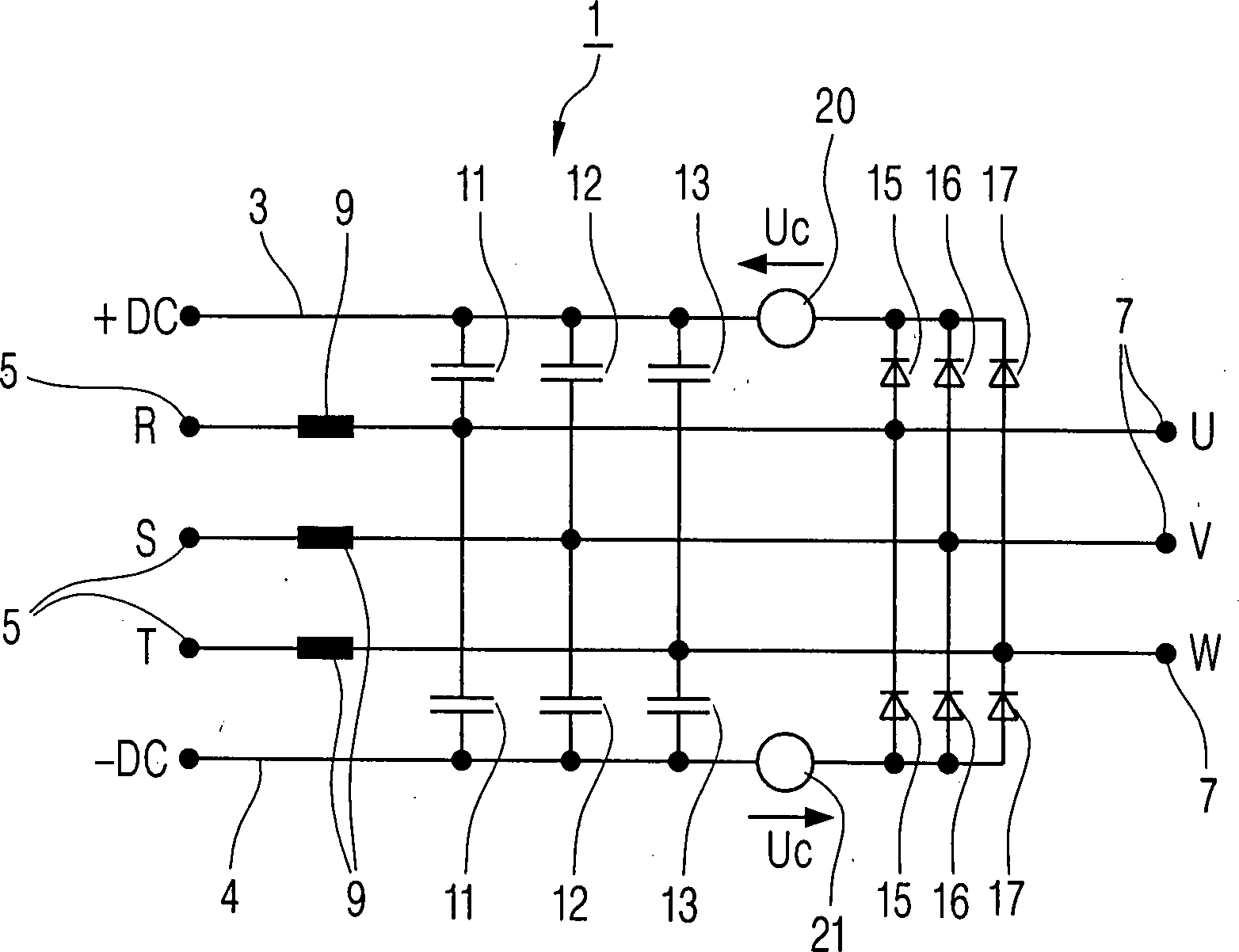
Schaltungsanordnung zur Vermeidung von Spannungsund/oder Stromspitzen in den Ausgangsleitungen eines Gleichspannungszwischenkreis gespeisten Umrichters, wobei die Ausgangsklemmen (5) des Umrichters jeweils über eine Induktivität (9) geführt und jeweils über einen Kondensator (11, 12, 13) und über eine zum Kondensator (11, 12, 13) parallel und bezüglich des Potenzials des Gleichspannungs-Zwischenkreises in Sperrrichtung geschaltete Diode (15, 16, 17) an das positive und an das negative Zwischenkreispotenzial angeschlossen sind, dadurch gekennzeichnet, dass zwischen die Diode (15, 16, 17) und dem Zwischenkreispotenzial jeweils eine das Zwischenkreispotenzial betragsmäßig erhöhende Gleichspannungsquelle (20, 21) eingeschaltet ist, und dass eine Rückspeiseschaltung (36) zur Einspeisung der in den Induktivitäten (9) zwischengespeicherten Energie in den Gleichspannungs-Zwischenkreis vorgesehen ist, wobei die Rückspeiseschaltung (36) mittels eines Brückenzweiges realisiert ist.circuitry to avoid voltage and / or current peaks in the output lines a DC voltage supplied converter, wherein the output terminals (5) of the inverter in each case via an inductance (9) out and each over a capacitor (11, 12, 13) and via a capacitor (11, 12, 13) 12, 13) parallel and with respect the potential of the DC link in the reverse direction switched diode (15, 16, 17) to the positive and to the negative DC link potential are connected, characterized that between the diode (15, 16, 17) and the DC link potential in each case a DC voltage source which increases the DC link potential in terms of magnitude (20, 21) is turned on, and that a feedback circuit (36) for Infeed of the inductively stored in the inductors (9) Energy in the DC link is provided, wherein the regenerative circuit (36) by means of a bridge branch is realized.
Description
Die Erfindung betrifft eine Schaltungsanordnung zur Vermeidung von Spannungs- und/oder Stromspitzen in den Ausgangsleitungen eines Umrichters.The The invention relates to a circuit arrangement for avoiding voltage and / or current spikes in the output lines of an inverter.
Ein Gleichspannungszwischenkreis gespeister Umrichter erzeugt durch intelligentes Zerhacken aus der Gleichspannung des Zwischenkreises eine Wechselspannung, wie sie zur Drehzahlsteuerung einer Drehfeldmaschine wie beispielsweise einem Elektromotor benötigt wird. Hierzu weist der Umrichter je nach Anzahl der von der Drehfeldmaschine benötigten Wechselspannungsphasen eine Anzahl von Funktionsbaugruppen auf, die einen steuerbaren Leistungshalbleiter und eine ihn überbrückende parallel geschaltete Freilaufdiode umfassen. In einer bekannten Schaltungsvariante sind jeweils zwei dieser Funktionsbaugruppen in Serie zwischen die Potenziale des Gleichspannungszwischenkreises geschaltet. Die von einer Drehfeldmaschine benötigte Ausgangsspannung wird in dieser Variante zwischen den Funktionsbaugruppen entnommen. Auf diese Weise fließt eine positive Halbwelle des Ausgangs- oder Verbraucherstroms durch den einen und eine negative Halbwelle durch den anderen Leistungshalbleiter bzw. durch die entsprechenden Freilaufdioden.One DC voltage supplied inverter generated by Intelligent chopping from the DC voltage of the DC link an alternating voltage, as used for speed control of a rotating field machine such as an electric motor is needed. For this purpose, the Inverter depending on the number of alternating voltage phases required by the induction machine a number of functional assemblies having a controllable power semiconductor and a bridging parallel comprise switched freewheeling diode. In a known circuit variant There are two of these function modules in series between the two Potentials of the DC intermediate circuit switched. The of an induction machine required Output voltage is in this variant between the function modules taken. This way flows a positive half wave of the output or consumer current through the one and a negative half-wave through the other power semiconductor or through the corresponding freewheeling diodes.
Als steuerbare Leitungshalbleiter für einen derartigen Umrichter haben sich heute Feldeffekt-Transistoren und insbesondere so genannte Insulated-Gate-Bipolar-Transistoren (IGBT's) durchgesetzt. Ein IGBT vereinigt dabei die Vorteile eines Feldeffekt-Transistors und eines Bipolartransistors und kann bei hohen Schaltgeschwindigkeiten mit niedrigen Schaltverlusten betrieben werden.When controllable line semiconductors for Such a converter today has field-effect transistors and in particular so-called insulated gate bipolar transistors (IGBT's) enforced. An IGBT combines the advantages of a field-effect transistor and a bipolar transistor and can at high switching speeds be operated with low switching losses.
Durch die hohen Schaltgeschwindigkeiten entstehen in den Ausgangsklemmen des Umrichters steile Spannungsflanken. Steile Spannungsflanken führen zu steilen Potenzialsprüngen in den Wicklungen einer angeschlossenen Drehfeldmaschine, wodurch das Isolationsmaterial der Wicklungen geschädigt oder zerstört werden kann. Insbesondere Drehfeldmaschinen älterer Bauart sind aufgrund der gegebenen Isolation daher für den Betrieb mit einem moderne Leistungshalbleiter aufweisenden Umrichter nicht geeignet. Weiter können steile Spannungsflanken insbesondere bei einem Anschluss der Drehfeldmaschine über ein längeres Anschlusskabel zu einem Schwingen der Leitung führen. An der Drehfeldmaschine selbst können dann Spannungen auftreten, die bis zum doppelten Wert der gewollten Ausgangsspannung überschwingen. Die Werte derartiger Überspannungsspitzen hängen dabei insbesondere von der Länge der Leitung und der Steilheit der Spannungsflanken ab. Die hohen Spannungen können unerwünschterweise zu einer Zerstörung der Wicklungen und in der Folge zur Zerstörung des Umrichters führen. Ebenfalls führen die aus den Überspannungen resultierenden hohen Ströme zu unerwünschten Problemen.By the high switching speeds occur in the output terminals the inverter steep voltage edges. Steep voltage edges lead to steep potential jumps in the windings of a connected induction machine, whereby the insulation material of the windings are damaged or destroyed can. In particular, rotary field machines of older design are due the given isolation therefore for the operation with a modern power semiconductors having inverter not suitable. Next you can steep voltage edges, especially when connecting the induction machine via a longer Lead the connecting cable to a swinging of the cable. At the induction machine yourself can then tensions occur that are up to twice the value of the desired Overshoot output voltage. The values of such overvoltage peaks hang especially the length the line and the slope of the voltage edges. The high Tensions can undesirably to a destruction the windings and subsequently lead to the destruction of the inverter. Also to lead those from the surges resulting high currents too unwanted Problems.
Zur
Vermeidung der durch steile Spannungsflanken hervorgerufenen Stromspitzen
in den Ausgangsleitungen eines Umrichters ist aus der
Weiter
ist aus der
Nachteiligerweise fließt bei einer derartigen Unterdrückungsschaltungen des Standes der Technik ein wesentlicher Teil des Freilaufstromes über die umfassten Dioden und nicht über die Freilaufdioden des Umrichters. Insbesondere ist dies der Fall, wenn den Induktivitäten zusätzlich ein ohmscher Widerstand unterstellt wird. Vor allem in einem generatorischen Betrieb der Drehfeldmaschine, in welcher der Motorstrom gegenüber der Ausgangsspannung des Umrichters phasenverschoben ist und durch die Freilaufdioden abfließt, führt dies dazu, dass am Umrichterausgang der dort gemessene Ausgangsstrom nicht mehr dem Motorstrom entspricht. Für eine sich am Motorstrom orientierende Regelung des Umrichters muss daher die Stromerfassung hinter die Unterdrückungsschaltung verlegt werden. Dies widerspricht dem Konzept eines modularen Aufbaues. Zusätzlich müssen die Dioden der Unterdrückungsschaltung überdimensioniert ausgelegt werden.Unfortunately, flows in such suppression circuits The prior art included a substantial portion of the freewheeling current over the Diodes and not over the freewheeling diodes of the inverter. In particular, this is the case if the inductors additionally an ohmic resistance is assumed. Especially in a generator Operation of the induction machine, in which the motor current relative to the Output voltage of the inverter is out of phase and through the Free-wheeling diodes flows off, does this In addition, the output current measured there at the inverter output does not more corresponds to the motor current. For a motor current orienting Control of the inverter must therefore the current detection behind the suppression circuit be moved. This contradicts the concept of a modular structure. additionally have to the diodes of the suppression circuit oversized be interpreted.
Aus
der
Weiter
ist aus der
Es ist Aufgabe der Erfindung, eine Schaltungsanordnung zur Vermeidung von Stromspitzen in den Ausgangsleitungen eines Gleichspannungszwischenkreis gespeisten Umrichters anzugeben, die die genannten Nachteile des Standes der Technik vermeidet.It Object of the invention, a circuit arrangement for the prevention of current peaks in the output lines of a DC intermediate circuit supplied inverter, the said disadvantages of the Prior art avoids.
Diese Aufgabe wird für eine Schaltungsanordnung der beschriebenen Art, wobei die Ausgangsklemmen des Umrichters jeweils über eine Induktivität geführt und jeweils über einen Kondensator und über eine zum Kondensator parallel und bezüglich des Potenzials des Gleichspannungszwischenkreises in Sperrrichtung geschaltete Diode an das positive und an das negative Zwischenkreispotenzial angeschlossen sind, erfindungsgemäß dadurch gelöst, dass zwischen die Diode und dem Zwischen kreispotenzial jeweils eine das Zwischenkreispotenzial betragsmäßig erhöhende Gleichspannungsquelle eingeschaltet ist.These Task is for a circuit arrangement of the type described, wherein the output terminals of the inverter respectively over an inductance guided and each about a capacitor and over one to the capacitor in parallel and with respect to the potential of the DC link reverse-connected diode to the positive and to the negative DC link potential are connected, according to the invention thereby solved that between the diode and the intermediate potential each one the DC link potential increasing the amount of DC voltage source is turned on.
Die Erfindung geht dabei von der Erkenntnis aus, dass sich der Freilaufstrom bei Unterdrückungsschaltungen des Standes der Technik auf die Freilaufdioden des Umrichters und die Dioden der Unterdrückungsschaltung aufteilt, da beide bezüglich der Ausgangsklemmen und dem Zwischenkreispotenzial parallel geschaltet sind. Diese den an den Ausgangsklemmen des Umrichters gemessenen Strom beeinflussende Aufteilung des Motorstroms kann verhindert werden, indem zwischen das Zwischenkreispotenzial und der Diode eine dem Freilaufstrom entgegenwirkende Gleichspannungsquelle geschaltet wird. Dies geschieht dadurch, dass die Gleichspannungsquelle so eingeschaltet ist, dass sie das Zwischenkreispotenzial betragsmäßig erhöht. Hierdurch wird verhindert, dass der Freilaufstrom über die Dioden der Unterdrückungsschaltung abfließt. Die Entladung der Induktivitäten erfolgt über die Gleichspannungsquellen und dauert nur kurz. Daher sind der an den Ausgangsklemmen des Umrichters gemessene Ausgangsstrom und der Motorstrom nahezu gleich groß.The The invention is based on the recognition that the freewheeling current in suppression circuits of the prior art to the freewheeling diodes of the inverter and the diodes of the suppression circuit divides, as both respect the output terminals and the DC link potential are connected in parallel are. These measured at the output terminals of the inverter Current influencing division of the motor current can be prevented by switching between the DC link potential and the diode a DC voltage source counteracting the freewheeling current is switched. This happens because the DC voltage source is turned on is that it increases the DC link potential in terms of amount. This will prevents the freewheeling current through the diodes of the suppression circuit flows. The discharge of the inductors over the DC sources and only takes a short time. Therefore, the to the Output terminals of the inverter measured output current and the motor current almost the same size.
Zum Aufbau der Gleichspannungsquelle genügen geringe Spannungen in der Größenordnung von 10 Volt. Die Unterdrückungsschaltung, die als ein du/dt-Filter arbeitet, kann additiv zum Umrichter angebaut werden, ohne die beispielsweise für eine Regelung erforderliche Strommessung aus dem Umrichter herauslösen zu müssen.To the Construction of the DC voltage source satisfy low voltages in the Order of magnitude 10 volts. The suppression circuit, which works as a du / dt filter can be added to the inverter without, for example, those required for a regulation To dissipate current measurement from the inverter.
Für eine Schaltungsvariante, die zur Unterdrückung des Abfließens des Freilaufstroms über die Dioden der Unterdrückungsschaltung Entkoppelkondensatoren verwendet, müssen diese eine erhebliche Kapazität aufweisen. Derartige Kondensatoren sind unerwünschterweise mit einem Kostenmehraufwand verbunden. Dieser Nachteil wird durch die Erfindung vermieden. For a circuit variant, to oppression the drain of freewheeling current over the diodes of the suppression circuit Decoupling capacitors used, these have a significant capacity exhibit. Such capacitors are undesirably expensive to pay connected. This disadvantage is avoided by the invention.
Ein weiterer Vorteil der Erfindung besteht darin, dass die Dioden der Unterdrückungsschaltung nicht überdimensioniert ausgelegt werden brauchen. Da der Freilaufstrom nicht mehr über die Dioden der Unterdrückungsschaltung abfließt, werden diese nur noch mit den für die Steilheitsbeschränkung der Unterdrückungsschaltung notwendigen Umschwingströme belastet.One Another advantage of the invention is that the diodes of Suppression circuit not oversized need to be interpreted. Since the free-wheeling current is no longer on the Diodes of the suppression circuit flows, these are only with the for the slope limitation the suppression circuit necessary Umschwingströme loaded.
Als ein Pufferkondensator in der Gleichspannungsquelle kann ein preisgünstiger Niedervolt-Kondensator, wie insbesondere ein Elektrolyt-Kondensator verwendet werden.When a buffer capacitor in the DC voltage source can be a cheaper Low-voltage capacitor, in particular an electrolytic capacitor be used.
Für die Erfindung spielt es keine Rolle, an welcher Stelle die Gleichspannungsquellen zwischen den Ausgangsklemmen und der Diode geschaltet sind. Aus schaltungstechnischen Gründen empfiehlt es sich, die Gleichspannungsquelle jeweils direkt an den Anschlusspunkten des Gleichspannungszwischenkreises vorzusehen. Sowohl der Kondensator als auch die parallel geschaltete Diode sind in dieser Variante schaltungstechnisch nach der Gleichspannungsquelle angeordnet.For the invention It does not matter at what point the DC sources are connected between the output terminals and the diode. Out circuit-technical reasons It is recommended that the DC voltage source directly to the Provide connection points of the DC voltage intermediate circuit. Both the capacitor and the parallel diode are in this variant circuitry according to the DC voltage source arranged.
Für jede von der Drehstrommaschine benötigte Phase des Umrichters wird bei der Unterdrückungsschaltung jeweils ein Kondensator und eine parallel geschaltete Diode zur schaltungstechnischen Verbindung mit dem positiven und zur schaltungstechnischen Verbindung mit dem negativen Zwischenkreispotenzial benötigt. Im Falle eines dreiphasigen Anschlusses zur Erzeugung eines Drehfeldes in der Drehfeldmaschine umfasst der Umrichter bei drei Anschlussklemmen insgesamt sechs der eingangs erwähnten Funktionsbaugruppen. Zum Aufbau der Unterdrückungsschaltung sind für jede der Anschlussklemmen eine Induktivität sowie zwei Kapazitäten und zwei Dioden erforderlich. Die Gleichspannungsquelle kann nun für jede der Dioden vorgesehen sein. Aus Kostengründen und aus Vereinfachungsgründen ist es jedoch von Vorteil, die Gleichspannungsquellen jeweils für die Dioden gleicher Polarität zusammenzufassen.For each of the three-phase machine needed Phase of the inverter is at the suppression circuit each one Capacitor and a parallel diode for circuit technology Connection with the positive and the circuit connection needed with the negative DC link potential. In the case of a three-phase Connection for generating a rotating field in the induction machine The inverter has a total of six at three terminals the aforementioned Function modules. To construct the suppression circuit are for each of the terminals an inductance as well as two capacities and two diodes required. The DC voltage source can now for every the diodes can be provided. For cost reasons and for reasons of simplification is However, it is advantageous, the DC sources for the diodes same polarity summarize.
In diesem Fall ist zwischen das jeweilige Zwischenkreispotenzial und den Dioden gleicher Polarität jeweils eine Gleichspannungsquelle eingeschaltet.In this case, a DC voltage source is switched on between the respective DC link potential and the diodes of the same polarity tet.
Die Gleichspannungsquelle kann grundsätzlich in verschiedenster Art und Weise realisiert werden. The DC voltage source can basically in a variety of ways and be realized.
Wird die Gleichspannungsquelle durch einen Widerstand realisiert, so wird die Rückspeise-Energie durch die abfließenden Entladeströme in Wärme umgesetzt. Für eine im Wesentlichen verlustlose Schaltungsanordnung ist eine Rückspeiseschaltung zur Einspeisung der in den Induktivitäten zwischengespeicherten Energie in den Gleichspannungszwischenkreis vorgesehen. Eine Rückspeiseschaltung verfälscht den an den Ausgangsklemmen des Umrichters gemessenen Stromwert nicht, da die Rückspeiseströme oder Entladeströme der Induktivitäten nicht über den Umrichter fließen.Becomes the DC voltage source realized by a resistor, so becomes the energy of return through the outflowing discharge converted into heat. For one essentially lossless circuitry is a regenerative circuit for Infeed of the energy stored in the inductors provided in the DC voltage intermediate circuit. A regenerative circuit distorts the current value measured at the output terminals of the inverter, because the regenerative currents or discharge the inductors do not have the Inverter flow.
Zur Ausgestaltung der Rückspeiseschaltung sind verschiedene Möglichkeiten vorstellbar. Beispielsweise kann die Gleichspannungsquelle selbst so ausgestaltet werden, dass sie die zwischengespeicherte Energie der Induktivitäten aufnehmen und wieder in den Zwischenkreis rückspeisen kann. to Design of the regenerative circuit are various possibilities imaginable. For example, the DC voltage source itself can be configured that they the cached energy of the inductors record and can feed back into the DC link.
Die Rückspeiseschaltung ist mittels eines Brückenzweiges realisiert. Dies ermöglicht sowohl eine Energierichtung in die Gleichspannungsquelle hinein als auch aus dieser heraus realisierbar.The Regenerative circuit is by means of a bridge branch realized. this makes possible both an energy direction in the DC voltage source inside as well as out of this feasible.
Ausführungsbeispiele der Erfindung werden anhand einer Zeichnung näher erläutert. Dabei zeigen:embodiments The invention will be explained in more detail with reference to a drawing. Showing:
In
Jede
der Ausgangsklemmen
Die
Schaltung
Von
dieser ersten Variante unterscheidet sich die in
In
In
dem Diagramm
Im
Vergleich zu
In
An den mit V und A bezeichneten Stellen werden Spannungen bzw. Ströme gemessen. Ein Rückspeisestrom wird mittels der Stromquelle I1 simuliert.At The points labeled V and A are used to measure voltages or currents. A regenerative current is simulated by means of the current source I1.
Die Leistungshalbleiter IBGT1 und IGBT2 werden mittels Pulsweitenmodulation getrieben, die symbolisch durch eine Steuerung PWM1, eine Konstantspannungsquelle CONST1 einen Addiererbaustein SUM1 und einen Negiererbaustein NEG1 repräsentiert sind.The power semiconductors IBGT1 and IGBT2 are driven by means of pulse width modulation, the symbolically represented by a controller PWM1, a constant voltage source CONST1, an adder component SUM1 and a negative component NEG1.
Umfangreiche Untersuchungen haben ergeben, dass sich bei einem Sprung in der Rückspeiseleitung mit einer derartigen Rückspeiseschaltung ein gedämpftes Verhalten erreichen lässt. Die Schaltfrequenz kann hoch gewählt werden, so dass die Bauelemente klein werden. Die erreichbare Dynamik wird dann hoch. Die pulsfrequenten Anteile der Rückspeiseschaltung können durch zusätzliche Filter herausgefiltert werden.extensive Research has shown that when jumping in the Rear feeder with such a feedback circuit a muted Achieve behavior. The switching frequency can be selected high so that the components become small. The achievable dynamics then gets high. The pulse-frequency components of the regenerative circuit can by additional Filter are filtered out.
Die rückgespeiste Leistung ist abhängig von der Dimensionierung der Rückspeiseschaltung, der Pulsfrequenz und der Höhe des Laststromes. Bei günstiger Auslegung fallen bei einem 200kW-Antrieb lediglich 10–20 Watt Rückspeiseleistung an (UC = 10 Volt, Pulsfrequenz = 1 kHz). Die Rückspeiseschaltung muss so ausgelegt sein, dass die anfallende Energie in den Zwischenkreis rückgespeist werden kann.The fed-back power depends on the dimensioning of the regenerative circuit, the pulse frequency and the magnitude of the load current. With a favorable design fall in a 200kW drive only 10-20 watts regenerative power (U C = 10 volts, pulse frequency = 1 kHz). The regenerative circuit must be designed so that the resulting energy can be fed back into the DC link.
Zur
Vermeidung von Schwingungsvorgängen
nach einem Stromabriss in den Dioden
Claims (3)
Priority Applications (1)
| Application Number | Priority Date | Filing Date | Title |
|---|---|---|---|
| DE200510045552 DE102005045552B4 (en) | 2005-09-23 | 2005-09-23 | circuitry |
Applications Claiming Priority (1)
| Application Number | Priority Date | Filing Date | Title |
|---|---|---|---|
| DE200510045552 DE102005045552B4 (en) | 2005-09-23 | 2005-09-23 | circuitry |
Publications (2)
| Publication Number | Publication Date |
|---|---|
| DE102005045552A1 DE102005045552A1 (en) | 2007-04-12 |
| DE102005045552B4 true DE102005045552B4 (en) | 2008-04-17 |
Family
ID=37886781
Family Applications (1)
| Application Number | Title | Priority Date | Filing Date |
|---|---|---|---|
| DE200510045552 Expired - Fee Related DE102005045552B4 (en) | 2005-09-23 | 2005-09-23 | circuitry |
Country Status (1)
| Country | Link |
|---|---|
| DE (1) | DE102005045552B4 (en) |
Cited By (3)
| Publication number | Priority date | Publication date | Assignee | Title |
|---|---|---|---|---|
| DE102008026869A1 (en) * | 2008-06-05 | 2009-12-10 | Siemens Aktiengesellschaft | Lossy three-phase low-pass filter |
| DE102018204090A1 (en) * | 2018-03-16 | 2019-09-19 | Schmidhauser Ag | Filter unit and frequency converter |
| DE102023201693A1 (en) | 2023-02-24 | 2024-08-29 | Robert Bosch Gesellschaft mit beschränkter Haftung | Filter device for an electric power converter, electric power converter and electric drive system |
Families Citing this family (1)
| Publication number | Priority date | Publication date | Assignee | Title |
|---|---|---|---|---|
| DE102006036092A1 (en) * | 2006-08-02 | 2008-02-07 | Siemens Ag | sine filter |
Citations (3)
| Publication number | Priority date | Publication date | Assignee | Title |
|---|---|---|---|---|
| EP0473192A2 (en) * | 1990-08-30 | 1992-03-04 | Mitsubishi Denki Kabushiki Kaisha | A circuit for reducing resonance voltage |
| DE4135680A1 (en) * | 1991-10-30 | 1993-05-06 | Andreas Prof. Dr.-Ing.Habil. 7000 Stuttgart De Boehringer | Inverter motor drive limiting rate of change of output currents - using inductive stages coupled between inverter outputs and motor units |
| DE9307806U1 (en) * | 1993-05-24 | 1993-08-26 | Siemens Ag | Inverter output filter |
-
2005
- 2005-09-23 DE DE200510045552 patent/DE102005045552B4/en not_active Expired - Fee Related
Patent Citations (3)
| Publication number | Priority date | Publication date | Assignee | Title |
|---|---|---|---|---|
| EP0473192A2 (en) * | 1990-08-30 | 1992-03-04 | Mitsubishi Denki Kabushiki Kaisha | A circuit for reducing resonance voltage |
| DE4135680A1 (en) * | 1991-10-30 | 1993-05-06 | Andreas Prof. Dr.-Ing.Habil. 7000 Stuttgart De Boehringer | Inverter motor drive limiting rate of change of output currents - using inductive stages coupled between inverter outputs and motor units |
| DE9307806U1 (en) * | 1993-05-24 | 1993-08-26 | Siemens Ag | Inverter output filter |
Cited By (7)
| Publication number | Priority date | Publication date | Assignee | Title |
|---|---|---|---|---|
| DE102008026869A1 (en) * | 2008-06-05 | 2009-12-10 | Siemens Aktiengesellschaft | Lossy three-phase low-pass filter |
| US8743572B2 (en) | 2008-06-05 | 2014-06-03 | Siemens Aktiengesellschaft | Lossy triphase low-pass filter |
| DE102008026869B4 (en) * | 2008-06-05 | 2014-11-20 | Siemens Aktiengesellschaft | Lossy three-phase low-pass filter |
| DE102018204090A1 (en) * | 2018-03-16 | 2019-09-19 | Schmidhauser Ag | Filter unit and frequency converter |
| EP3766171A1 (en) * | 2018-03-16 | 2021-01-20 | Schmidhauser AG | Filter unit and frequency inverter |
| US11374485B2 (en) | 2018-03-16 | 2022-06-28 | Schmidhauser Ag | Filter unit and frequency inverter |
| DE102023201693A1 (en) | 2023-02-24 | 2024-08-29 | Robert Bosch Gesellschaft mit beschränkter Haftung | Filter device for an electric power converter, electric power converter and electric drive system |
Also Published As
| Publication number | Publication date |
|---|---|
| DE102005045552A1 (en) | 2007-04-12 |
Similar Documents
| Publication | Publication Date | Title |
|---|---|---|
| DE60027538T2 (en) | Overvoltage-protected current inverter with a voltage-controlled circuit | |
| DE102008032876B4 (en) | Method, circuit arrangement and bridge circuit | |
| DE69805675T2 (en) | Power supply for control circuit | |
| EP2654190B1 (en) | Method for operating an electric circuit | |
| DE102013002266A1 (en) | Bootstrap Circuitry for an IGBT | |
| EP1715582B1 (en) | Circuit arrangement for driving an electric power switch at high voltage | |
| DE102018001032A1 (en) | Motor driving device | |
| DE102005045552B4 (en) | circuitry | |
| EP0743126B1 (en) | Arc welding device with improved dynamic characteristics | |
| AT409318B (en) | PROTECTIVE CIRCUIT FOR A NETWORKED THYRISTOR BRIDGE | |
| EP1564618B1 (en) | Circuit for power factor correction in switching power supplies, chargers and the like | |
| DE19731836A1 (en) | Method and device for driving a shutdown thyristor | |
| EP0751611B1 (en) | Power converter circuit | |
| WO2020239797A1 (en) | Circuit arrangement comprising at least one half-bridge | |
| DE102005019215A1 (en) | Output filter for e.g. pulsed power converter, has filter chokes and filter condensers, which are interconnected as LC low pass, and circuit arrangement for dynamically and continuously reducing effectiveness of filter chokes and condensers | |
| DE102013218799A1 (en) | Modular power converter | |
| DE102008019294A1 (en) | Supply unit for electric drives and method for controlling this supply unit | |
| DE10336287B4 (en) | Mains filter and power supply device | |
| EP1495525A2 (en) | Device for the inductive transmission of electric power | |
| DE3880621T2 (en) | VOLTAGE LIMITATION CIRCUIT FOR POWER TRANSISTOR AND INVERTER. | |
| DE2445073A1 (en) | FEED CIRCUIT | |
| DE10248971A1 (en) | AC powered motor frequency converter especially for elevators and lifting equipment, has low-pass setter connected between rectifier and intermediate circuit | |
| EP3192173B1 (en) | Half bridge having two semiconductor switches for operating a load | |
| DE19848728B4 (en) | Converter device for a DC machine | |
| EP3673551B1 (en) | Voltage supply circuit |
Legal Events
| Date | Code | Title | Description |
|---|---|---|---|
| OP8 | Request for examination as to paragraph 44 patent law | ||
| 8364 | No opposition during term of opposition | ||
| R119 | Application deemed withdrawn, or ip right lapsed, due to non-payment of renewal fee |