EP0468209A2 - Translateur de niveau à commande unique, à faible impédance dynamique - Google Patents
Translateur de niveau à commande unique, à faible impédance dynamique Download PDFInfo
- Publication number
- EP0468209A2 EP0468209A2 EP91110382A EP91110382A EP0468209A2 EP 0468209 A2 EP0468209 A2 EP 0468209A2 EP 91110382 A EP91110382 A EP 91110382A EP 91110382 A EP91110382 A EP 91110382A EP 0468209 A2 EP0468209 A2 EP 0468209A2
- Authority
- EP
- European Patent Office
- Prior art keywords
- transistor
- level shifter
- output
- inverter
- signal level
- Prior art date
- Legal status (The legal status is an assumption and is not a legal conclusion. Google has not performed a legal analysis and makes no representation as to the accuracy of the status listed.)
- Granted
Links
Images

Classifications
-
- H—ELECTRICITY
- H04—ELECTRIC COMMUNICATION TECHNIQUE
- H04L—TRANSMISSION OF DIGITAL INFORMATION, e.g. TELEGRAPHIC COMMUNICATION
- H04L25/00—Baseband systems
- H04L25/02—Details ; arrangements for supplying electrical power along data transmission lines
- H04L25/03—Shaping networks in transmitter or receiver, e.g. adaptive shaping networks
-
- H—ELECTRICITY
- H03—ELECTRONIC CIRCUITRY
- H03K—PULSE TECHNIQUE
- H03K17/00—Electronic switching or gating, i.e. not by contact-making and –breaking
- H03K17/06—Modifications for ensuring a fully conducting state
-
- H—ELECTRICITY
- H03—ELECTRONIC CIRCUITRY
- H03K—PULSE TECHNIQUE
- H03K17/00—Electronic switching or gating, i.e. not by contact-making and –breaking
- H03K17/04—Modifications for accelerating switching
- H03K17/041—Modifications for accelerating switching without feedback from the output circuit to the control circuit
- H03K17/0412—Modifications for accelerating switching without feedback from the output circuit to the control circuit by measures taken in the control circuit
- H03K17/04123—Modifications for accelerating switching without feedback from the output circuit to the control circuit by measures taken in the control circuit in field-effect transistor switches
-
- H—ELECTRICITY
- H03—ELECTRONIC CIRCUITRY
- H03K—PULSE TECHNIQUE
- H03K17/00—Electronic switching or gating, i.e. not by contact-making and –breaking
- H03K17/06—Modifications for ensuring a fully conducting state
- H03K17/063—Modifications for ensuring a fully conducting state in field-effect transistor switches
Definitions
- the present invention relates to a single-drive level shifter, with low dynamic impedance.
- the invention relates to such a single-drive level shifter which is suitable for being implemented in integrated form in CMOS technology.
- the invention relates to an improved level shifter for driving power stages for supplying power to integrated circuits.
- CMOS complementary metal-oxide-semiconductor
- DMOS double-diffusion MOS
- FIG. 1 A schematic example of such a circuit is illustrated in Figure 1, wherein two DMOS transistors 10 and 12, provided with resistive loads 14 and 16, with voltage-limiting Zener diodes 18 and 20, drive the set and reset inputs of a flip-flop 22, the output whereof drives a driver 24 for a power stage which is not illustrated. Since either of resistors 14 and 16 carries current in any operating condition, circuits of this type have an undesirable continuous dissipation, besides occupying a large semiconductor area. Circuital variations have been proposed wherein the passive loads are replaced with active loads, in order to avoid continuous dissipation, but at the expense of a greater circuital complexity which further aggravates the problem of area occupation.
- DMOS transistor 26 with a load constituted by a resistor 28 and by a Zener diode 30 arranged in parallel, drives an inverter driver 32 which drives a power transistor 34.
- the current pulse generated by the transistor 26 causes switching "on", whereas for switching "off” it is necessary to wait for the increase in the voltage of the drain of the transistor 26, i.e. of the node V1, with respect to the node V2.
- This voltage increase is controlled by the discharge of the parasitic capacitor 36 between the drain and the source of the transistor 34, and this leads to a delay with respect to double-drive circuits, especially during switching "on". This delay can be decreased by reducing the switching threshold of the following stage or by reducing the load resistor or the parasitic capacitor.
- the above known circuits have another, subtler, disadvantage, especially for systems in which the supply voltage on the elements which are powered at switching "on", should not have a high slope.
- an excessively high slope dV/dt of the voltage can produce an injection of current in the parasitic capacitor of the DMOS transistor, which by passing in the load (whether active or passive) creates an unwanted voltage drop which can cause the early switching of the system, i.e.
- Spurious switching "on” of the system could be eliminated by reducing the resistive value of the load, but with the consequence of further increasing dissipation.
- a single drive signal level shifter comprising first and second transistors, each having a drain, a gate and a source, said first transistor being a DMOS transistor, said second transistor being a MOS transistor; a signal source, said signal source being connected to the gate of said first transistor; a voltage source; a load element; said first transistor being connected to said load element in series with each other and with said voltage source; said second transistor being connected in parallel with said load element; an inverter having an input and an output, the input of said inverter being connected to the connection of said first transistor to said load element; a drive stage having an input and an output, the input of said drive stage being connected to the output of said inverter; the gate of said second transistor being connected to the output of said inverter.
- a single drive DMOS transistor driven by a digital signal, has a load resistor as its drain load, with a Zener diode connected in parallel with the load resistor, with a shifted output signal developing at the ends of the load resistor.
- the drain of the DMOS transistor is connected to the input of the inverter.
- the second transistor is a P-channel transistor arranged in parallel with the load resistor, with the gate of the P-channel transistor being driven by the output of the inverter.
- the P-channel transistor has a significantly lower resistance than the load resistor.
- the output of the inverter is connected to the input of a drive circuit which drives a power circuit for supplying power to integrated circuits.
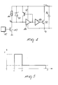
- a DMOS transistor 40 receives a digital signal from a digital signal source 42.
- the DMOS transistor 40 and a load resistor 44 are connected in series with each other between a voltage reference ground and a high voltage source V cc , with the source of the transistor 40 being connected to the voltage reference ground, such that resistor 44 serves as a drain load for transistor 40.
- the resistor 44 has a relatively high value, for example twenty kohm.
- the drain V1 of the DMOS transistor 40 drives an inverter 46,the output of the inverter 46 in turn drives a driver stage 48 for driving a power transistor 50 which is powered by the floating voltage between V cc and V2.
- a P-channel transistor 52 is connected in parallel to the resistor 44 and is dimensioned so as to have a low conduction resistance, for example one kohm.
- the gate of the transistor 52 is driven by the output of the inverter 46.
- a Zener diode 54 is connected in parallel to the transistor 52 and the load resistor 44.
- the transistor 40 In the absence of a digital signal at the input gate of the DMOS transistor 40, the transistor 40 is "off", its drain is high, and the output of the inverter 46 is low. The P-channel transistor 52 is thus "on”.
- the digital signal source 42 applies an impulse to the gate of the DMOS transistor 40, the voltage on the drain of transistor 40 drops, and thus the output of the inverter 46 tends to rise, leading the P-channel transistor 52 toward the switching "off” condition.
- a positive feedback is triggered which facilitates switching, because the impedance of the load on the DMOS transistor 40 tends to increase (due to the switching "off” of the transistor 52), and thus the voltage of the drain of the DMOS transistor 40 tends to decrease and the output of the inverter 46 tends to increase.
- the power transistor 50 thus switches “on”, and once it is “on”, a low current in the resistor 42 is sufficient to maintain this condition.
- Fig. 5 illustrates the qualitative behavior of the current I in the DMOS transistor 40 as a function of the time t, where the point C is the instant at which the drive signal is applied from the source 42 and the point D is the instant at which switching is completed.
- the switching-off time constant is the one given by the parasitic capacitor 56. In this case, too, however, a positive feedback is triggered which accelerates switching by acting on the P-channel transistor 52.
- the transistor 52 since the transistor 52 has a low resistance, which is determined by its dimensions, the voltage drop on it, due to the dV/dt derivative in output, can be controlled so as to not cause the early switching "on" of the power transistor 50.
Applications Claiming Priority (2)
| Application Number | Priority Date | Filing Date | Title |
|---|---|---|---|
| IT02108690A IT1243691B (it) | 1990-07-27 | 1990-07-27 | Traslatore di livello a transistore singolo, con bassa impedenza dinamica, in tecnologia cmos |
| IT2108690 | 1990-07-27 |
Publications (3)
| Publication Number | Publication Date |
|---|---|
| EP0468209A2 true EP0468209A2 (fr) | 1992-01-29 |
| EP0468209A3 EP0468209A3 (en) | 1992-04-29 |
| EP0468209B1 EP0468209B1 (fr) | 1995-08-16 |
Family
ID=11176523
Family Applications (1)
| Application Number | Title | Priority Date | Filing Date |
|---|---|---|---|
| EP91110382A Expired - Lifetime EP0468209B1 (fr) | 1990-07-27 | 1991-06-24 | Translateur de niveau à commande unique, à faible impédance dynamique |
Country Status (6)
| Country | Link |
|---|---|
| US (1) | US5160854A (fr) |
| EP (1) | EP0468209B1 (fr) |
| JP (1) | JPH04234216A (fr) |
| KR (1) | KR920003703A (fr) |
| DE (1) | DE69112153T2 (fr) |
| IT (1) | IT1243691B (fr) |
Cited By (1)
| Publication number | Priority date | Publication date | Assignee | Title |
|---|---|---|---|---|
| WO2000025424A1 (fr) * | 1998-10-23 | 2000-05-04 | Koninklijke Philips Electronics N.V. | Commutateur de niveaux |
Families Citing this family (5)
| Publication number | Priority date | Publication date | Assignee | Title |
|---|---|---|---|---|
| ITMI20010159A1 (it) * | 2001-01-29 | 2002-07-29 | Stmicroelettronica S R L | Circuito traslatore ad alta tensione con tempo di risposta ottimizzato |
| US7239178B1 (en) * | 2004-03-23 | 2007-07-03 | Cypress Semiconductor Corp. | Circuit and method for CMOS voltage level translation |
| JP5881432B2 (ja) * | 2012-01-20 | 2016-03-09 | 新日本無線株式会社 | レベル変換回路 |
| CN107005232B (zh) | 2014-11-26 | 2021-01-26 | 硅工厂股份有限公司 | 具有改进的时间响应特性的通路开关电路及其控制方法 |
| WO2016114415A1 (fr) | 2015-01-13 | 2016-07-21 | 주식회사 실리콘웍스 | Circuit de décalage de niveau à caractéristiques de réponse temporelle améliorées et son procédé de commande |
Citations (4)
| Publication number | Priority date | Publication date | Assignee | Title |
|---|---|---|---|---|
| FR2296307A1 (fr) * | 1974-12-24 | 1976-07-23 | Ibm | Circuits a resistance negative a dispositifs mos complementaires |
| US4347445A (en) * | 1979-12-31 | 1982-08-31 | Exxon Research And Engineering Co. | Floating hybrid switch |
| WO1990000328A1 (fr) * | 1988-07-01 | 1990-01-11 | Viteq Corporation | Decaleur de niveaux avec immunite en mode commun eleve |
| EP0388616A2 (fr) * | 1989-03-08 | 1990-09-26 | Hitachi, Ltd. | Circuit de protection à maximum d'intensité pour un dispositif électrostatique à débrayage automatique |
Family Cites Families (7)
| Publication number | Priority date | Publication date | Assignee | Title |
|---|---|---|---|---|
| JPS5891680A (ja) * | 1981-11-26 | 1983-05-31 | Fujitsu Ltd | 半導体装置 |
| US4501978A (en) * | 1982-11-24 | 1985-02-26 | Rca Corporation | Level shift interface circuit |
| US4791323A (en) * | 1986-10-23 | 1988-12-13 | Silicon Systems, Inc. | Level translation circuit |
| US4829203A (en) * | 1988-04-20 | 1989-05-09 | Texas Instruments Incorporated | Integrated programmable bit circuit with minimal power requirement |
| US4958091A (en) * | 1988-06-06 | 1990-09-18 | Micron Technology, Inc. | CMOS voltage converter |
| US4958089A (en) * | 1988-12-20 | 1990-09-18 | Gazelle Microcircuits, Inc. | High output drive FET buffer for providing high initial current to a subsequent stage |
| US5036226A (en) * | 1989-10-23 | 1991-07-30 | Ncr Corporation | Signal converting circuit |
-
1990
- 1990-07-27 IT IT02108690A patent/IT1243691B/it active IP Right Grant
-
1991
- 1991-06-24 DE DE69112153T patent/DE69112153T2/de not_active Expired - Fee Related
- 1991-06-24 EP EP91110382A patent/EP0468209B1/fr not_active Expired - Lifetime
- 1991-07-19 JP JP3179723A patent/JPH04234216A/ja active Pending
- 1991-07-24 KR KR1019910012663A patent/KR920003703A/ko not_active Application Discontinuation
- 1991-07-24 US US07/734,911 patent/US5160854A/en not_active Expired - Lifetime
Patent Citations (4)
| Publication number | Priority date | Publication date | Assignee | Title |
|---|---|---|---|---|
| FR2296307A1 (fr) * | 1974-12-24 | 1976-07-23 | Ibm | Circuits a resistance negative a dispositifs mos complementaires |
| US4347445A (en) * | 1979-12-31 | 1982-08-31 | Exxon Research And Engineering Co. | Floating hybrid switch |
| WO1990000328A1 (fr) * | 1988-07-01 | 1990-01-11 | Viteq Corporation | Decaleur de niveaux avec immunite en mode commun eleve |
| EP0388616A2 (fr) * | 1989-03-08 | 1990-09-26 | Hitachi, Ltd. | Circuit de protection à maximum d'intensité pour un dispositif électrostatique à débrayage automatique |
Cited By (1)
| Publication number | Priority date | Publication date | Assignee | Title |
|---|---|---|---|---|
| WO2000025424A1 (fr) * | 1998-10-23 | 2000-05-04 | Koninklijke Philips Electronics N.V. | Commutateur de niveaux |
Also Published As
| Publication number | Publication date |
|---|---|
| EP0468209A3 (en) | 1992-04-29 |
| IT1243691B (it) | 1994-06-21 |
| KR920003703A (ko) | 1992-02-29 |
| DE69112153T2 (de) | 1996-04-18 |
| DE69112153D1 (de) | 1995-09-21 |
| IT9021086A1 (it) | 1992-01-27 |
| IT9021086A0 (it) | 1990-07-27 |
| US5160854A (en) | 1992-11-03 |
| JPH04234216A (ja) | 1992-08-21 |
| EP0468209B1 (fr) | 1995-08-16 |
Similar Documents
| Publication | Publication Date | Title |
|---|---|---|
| KR900004590B1 (ko) | 출력 버퍼회로 | |
| US6407594B1 (en) | Zero bias current driver control circuit | |
| US5281862A (en) | Power MOSFET driver with cross-conduction current reduction | |
| US4866304A (en) | BICMOS NAND gate | |
| US6646469B2 (en) | High voltage level shifter via capacitors | |
| US4504779A (en) | Electrical load drive and control system | |
| US4459498A (en) | Switch with series-connected MOS-FETs | |
| US5781045A (en) | Method and apparatus for predriving a driver circuit for a relatively high current load | |
| EP0763882A1 (fr) | Dispositif d'attaque de charge | |
| US4590395A (en) | FET-bipolar drive circuit | |
| EP0351820B1 (fr) | Circuit de sortie | |
| JP2892815B2 (ja) | Igbtの駆動回路 | |
| US5204562A (en) | Turn off delay reduction circuit and method | |
| US5057721A (en) | Level shift circuit for controlling a driving circuit | |
| EP0468209B1 (fr) | Translateur de niveau à commande unique, à faible impédance dynamique | |
| JPH1075164A (ja) | 電圧制御形スイッチング素子のゲート駆動回路 | |
| US3396314A (en) | Overdrive circuit for inductive loads | |
| US4967100A (en) | Capacitive load driving apparatus | |
| US5166551A (en) | High speed output circuit without fluctuation for semiconductor integrated circuits | |
| US5146109A (en) | Circuit for driving a floating circuit in response to a digital signal | |
| JP3258050B2 (ja) | 誘導性負荷用mosfetを備えた回路装置 | |
| EP0620646B1 (fr) | Circuit de commande à courant de polarisation nul pour un circuit d'attaque de type low-side | |
| US5408136A (en) | Circuit for providing fast logic transitions | |
| US5166544A (en) | Pseudo Darlington driver acts as Darlington during output slew, but has only 1 VBE drop when fully turned on | |
| US6169441B1 (en) | Drive circuit for a field effect-controlled power semiconductor component |
Legal Events
| Date | Code | Title | Description |
|---|---|---|---|
| PUAI | Public reference made under article 153(3) epc to a published international application that has entered the european phase |
Free format text: ORIGINAL CODE: 0009012 |
|
| AK | Designated contracting states |
Kind code of ref document: A2 Designated state(s): DE FR GB NL SE |
|
| PUAL | Search report despatched |
Free format text: ORIGINAL CODE: 0009013 |
|
| AK | Designated contracting states |
Kind code of ref document: A3 Designated state(s): DE FR GB NL SE |
|
| RAP1 | Party data changed (applicant data changed or rights of an application transferred) |
Owner name: SGS-THOMSON MICROELECTRONICS S.R.L. |
|
| 17P | Request for examination filed |
Effective date: 19920922 |
|
| 17Q | First examination report despatched |
Effective date: 19941021 |
|
| GRAA | (expected) grant |
Free format text: ORIGINAL CODE: 0009210 |
|
| AK | Designated contracting states |
Kind code of ref document: B1 Designated state(s): DE FR GB NL SE |
|
| PG25 | Lapsed in a contracting state [announced via postgrant information from national office to epo] |
Ref country code: NL Free format text: LAPSE BECAUSE OF FAILURE TO SUBMIT A TRANSLATION OF THE DESCRIPTION OR TO PAY THE FEE WITHIN THE PRESCRIBED TIME-LIMIT Effective date: 19950816 |
|
| REF | Corresponds to: |
Ref document number: 69112153 Country of ref document: DE Date of ref document: 19950921 |
|
| PG25 | Lapsed in a contracting state [announced via postgrant information from national office to epo] |
Ref country code: SE Effective date: 19951116 |
|
| ET | Fr: translation filed | ||
| NLV1 | Nl: lapsed or annulled due to failure to fulfill the requirements of art. 29p and 29m of the patents act | ||
| PLBE | No opposition filed within time limit |
Free format text: ORIGINAL CODE: 0009261 |
|
| STAA | Information on the status of an ep patent application or granted ep patent |
Free format text: STATUS: NO OPPOSITION FILED WITHIN TIME LIMIT |
|
| 26N | No opposition filed | ||
| PGFP | Annual fee paid to national office [announced via postgrant information from national office to epo] |
Ref country code: FR Payment date: 20000612 Year of fee payment: 10 |
|
| PGFP | Annual fee paid to national office [announced via postgrant information from national office to epo] |
Ref country code: DE Payment date: 20000619 Year of fee payment: 10 |
|
| PGFP | Annual fee paid to national office [announced via postgrant information from national office to epo] |
Ref country code: GB Payment date: 20000621 Year of fee payment: 10 |
|
| PG25 | Lapsed in a contracting state [announced via postgrant information from national office to epo] |
Ref country code: GB Free format text: LAPSE BECAUSE OF NON-PAYMENT OF DUE FEES Effective date: 20010624 |
|
| GBPC | Gb: european patent ceased through non-payment of renewal fee |
Effective date: 20010624 |
|
| PG25 | Lapsed in a contracting state [announced via postgrant information from national office to epo] |
Ref country code: FR Free format text: LAPSE BECAUSE OF NON-PAYMENT OF DUE FEES Effective date: 20020228 |
|
| PG25 | Lapsed in a contracting state [announced via postgrant information from national office to epo] |
Ref country code: DE Free format text: LAPSE BECAUSE OF NON-PAYMENT OF DUE FEES Effective date: 20020403 |