EP0466968A1 - Thermal recording system and thermal recording head - Google Patents
Thermal recording system and thermal recording head Download PDFInfo
- Publication number
- EP0466968A1 EP0466968A1 EP90113981A EP90113981A EP0466968A1 EP 0466968 A1 EP0466968 A1 EP 0466968A1 EP 90113981 A EP90113981 A EP 90113981A EP 90113981 A EP90113981 A EP 90113981A EP 0466968 A1 EP0466968 A1 EP 0466968A1
- Authority
- EP
- European Patent Office
- Prior art keywords
- recording
- heating elements
- terminals
- line
- recording head
- Prior art date
- Legal status (The legal status is an assumption and is not a legal conclusion. Google has not performed a legal analysis and makes no representation as to the accuracy of the status listed.)
- Granted
Links
Images


Classifications
-
- B—PERFORMING OPERATIONS; TRANSPORTING
- B41—PRINTING; LINING MACHINES; TYPEWRITERS; STAMPS
- B41J—TYPEWRITERS; SELECTIVE PRINTING MECHANISMS, i.e. MECHANISMS PRINTING OTHERWISE THAN FROM A FORME; CORRECTION OF TYPOGRAPHICAL ERRORS
- B41J2/00—Typewriters or selective printing mechanisms characterised by the printing or marking process for which they are designed
- B41J2/315—Typewriters or selective printing mechanisms characterised by the printing or marking process for which they are designed characterised by selective application of heat to a heat sensitive printing or impression-transfer material
- B41J2/32—Typewriters or selective printing mechanisms characterised by the printing or marking process for which they are designed characterised by selective application of heat to a heat sensitive printing or impression-transfer material using thermal heads
- B41J2/345—Typewriters or selective printing mechanisms characterised by the printing or marking process for which they are designed characterised by selective application of heat to a heat sensitive printing or impression-transfer material using thermal heads characterised by the arrangement of resistors or conductors
Definitions
- the present invention relates to a method for arranging a higher density and less cost thermal- recording head.
- the thermal recording system includes a recording unit operated in a serial printer or line printer mode.
- the serial-printer-mode recording unit employs a recording head consisting of at most one hundred heating elements.
- the line-printer-mode recording unit requires a recording head consisting of several thousands of heating resistive elements ranged in a line. In order to heat such a great number of heating elements in response to a recording signal, the following types of recording heads were developed; 1. Diode Matrix Type
- this type of recording head has been employed in a facsimile. It results in giving an opportunity of developing a thermal recording system.
- the diode matrix type recording head is designed to use a group of 32 to 64 heating elements as a single unit for recording. It thus takes several hundred mm seconds in recording one line. For reducing the recording time of one line to several mm seconds by concurrently heating many heating elements, developed are: 2. Thyristor Alloy Type and 3. Semiconductor IC Mount Type. Today, the thermal recording system normally employs a semiconductor IC mount type for thermal printing.
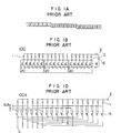
- Figs. 1A to 1D show circuit arrangement of a recording pattern, arrangement of a heating section and an overall recording head used in a conventional semiconductor IC mount type recording head.
- Fig. 1A shows a recording pattern used in the conventional recording head, wherein 18 resistive segments ranged in a line are divided in three groups for recording.
- the conventional semiconductor IC mount type recording head as shown in Fig. 1A, is designed to divide the eighteen resistive segments into three groups, each of which is a single recording unit consisting of adjacent six segments. Since the eighteen heating elements are ranged exactly in a line, the divisional recording system slightly shifts recording positions of second and third recorded dots relative to the recording position of the first recorded dots in the feeding direction of the recording paper.
- Fig. 1 B shows arrangement of the heating unit of the conventional semiconductor IC mount type recording head.
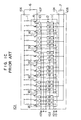
- Fig. 1 C shows an example of overall circuit illustrating the conventional IC-type head, wherein;
- the IC circuit 20 comparises
- the terminals of the semiconductor IC 20 are respectively connected to the eighteen elements 1 as shown for forming recording head actuating terminals 101 a, c to 107.
- the terminals 104 and 105 are connected to the semiconductor IC power source 7.
- the recording head is designed to apply a one-line recording signal to the terminal 101a, transfer the recording signal sequentially through the eighteen shift register circuits 11 in response to a clock signal from the terminal 101b, and temporarily store the recording signal transferred by a latch signal from the terminal 102 in the eighteen latch circuits 12.
- the first to sixth transistors 4 As viewed from the right hand become conductive in response to the recording signals stored in the corresponding latch circuits. Then, the six heating elements 1 connected to the conductive transistors 4 are heated up by the power source 6 for actuating the heating elements, the power source being connected to the terminals 106 and 107. Succeeding to a signal application to the terminals 103b and 103c, the seventh to twelfth and the thirteenth to eighteenth heating elements are heated up, resulting in the one-line recording as shown in Fig. 1.
- the next line signal is applied to the terminal 101a a for preparing the succeeding next line recording.
- the subsequent lines are recorded in the divisional recording mode.
- 104 and 105 denote semiconductor IC power terminals of the recording head.
- the shortcoming of the arrangement of the heating unit shown in Fig.1 B is to require connection of heating resistive elements to semiconductor devices (diode array, thyristor array or output transistor array) in one-to-one relationship by a high density lead line pattern. That is, the manufacture of a heating element actuating type recording head as shown in Fig. 1B becomes more difficult as the array density of the heating elements becomes higher.
- the present invention is implemented for the main purposes of:
- the present invention employs a novel divisional recording system of heating elements. That is, the invention comprises;
- Fig. 2A shows a one-line recording pattern formed in the case where a divisional recording system of the invention performs recording by dividing eighteen resistors ranged in a line into three groups.
- the way of illustration of Fig. 2A is similar to that in Fig. 1A.
- the present invention is designed to actuate, at first, a first group of the first, 4-th, 7-th, 10-th, 13-th and 16-th resistors for recording the corresponding dots as viewed from the left hand and then repeat the similar divisional recording twice.
- the present recording system is more likely to shift the recording dots out of proper positions than the conventional recording system. This shortcoming can be prevented by shifting the heating element arrangement in the travelling direction of the recording paper.
- Figs. 2B and 2C show arrangements of two heating units according to the present invention for performing the divisional recording described with reference to Fig. 2A.
- Fig. 2B shows a heating unit 200 employing a common electrode divisional system according to the invention.
- This heating unit comprises heating elements 1 ranged in one line,
- Fig. 2C shows a heating unit 300 employing a switching element system according to the invention.
- the heating unit comprises a plurality of heating elements 1 and switching elements 5 (for example, field-effect transistors) ranged in one line,
- the present invention reduces the number of transistors 4 mounted therein to 1/divisional number of recordings.
- this invention reduces the number of transistors included therein more greatly than the conventional recording head arrangement. It is thus possible to achieve the main purposes of the invention, that is, high recording density and less costly recording head.
- the recording head is made less costly by reducing to 1/N
- Fig. 1D shows arrangement of a switching element system heating unit employing the conventional divisional recording system.
- the function of each terminal is similar to that shown in Fig. 2B.
- these terminals referenced by like numerals are not explained.
- the conventional divisional recording system for the heating elements is designed to disperse to various locations the heating elements are connected to the individual terminals 3 on the overall width.
- the connection of a leading wire for forming individual terminals is made surprisingly more complicated. It is a great obstacle to the arrangement of a concrete head.
- the divisional recording system of the invention described with reference to Fig. 2A is an indispensable method for reducing the number of semiconductor ICs and leading wires of the semiconductor ICs.
- the recording head of the invention may be arranged by the conventional semiconductor IC 20. This recording head, however, requires the change of a transferring order of a recording signal outside of itself.
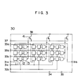
- Fig. 3 is a circuit diagram of a semiconductor IC according to the present invention.
- the semiconductor IC is arranged to change the order of a recording signal for the conventional recording head inside of it and actuate the heating elements in the order shown in Fig. 2B.
- Fig. 3 shows a circuit diagram showing an overall semiconductor IC 30 according to the invention. Like the conventional semiconductor IC, this semiconductor IC comprises
- the semiconductor IC has three functions of:
- the semiconductor IC 30 has a somewhat enlarged chip size because of a large number of circuits (shiftregister 11, latch 12 and gate 13), though, it is still practical in that;
- the present embodiment describes the common electrode division type head according to the invention.
- the recording head mounts the semiconductor ICs 30 by wire-bonding technique.
- Fig. 4A is a circuit illustration showing a common electrode division type head 200 employing the semiconductor ICs 30 according to the invention.
- the terminals of the semiconductor ICs 30 are respectively connected to eighteen resistors 1 for forming recording operation terminals 201 a, c to 207.
- the recording head shown in Fig. 4A operates to;
- the recording head shown in Fig. 4A is arranged to synchronize the switching connection of the terminals 204a, b, c to the power source and the switching operation of the gate signal by the connection of the three common electrodes 204a, b, c respectively to the gate signal terminals 33a, b, c.
- 6R denotes a resistor, which serves to adjust a voltage level of the gate signal for the synchronization by the above connection.
- 205 denotes a terminal led to the power source for actuating the heating elements.
- 206 and 207 each denotes a terminal led to a semiconductor IC power source.
- the recording head of this embodiment can be operated similarly with the conventional semiconductor IC type recording head by the same recording signal as conventional IC-type head.
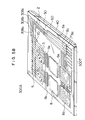
- Fig. 4B shows the concrete structure of the recording head 200 having semiconductor ICs mounted by a wire-bonding technique.
- 200A is a view showing an overall recording head and 200T is a view showing a group of terminals provided in the recording head, wherein
- the recording head shown in Fig. 4B comprises a substrate 50 on which a thermal and electric insulating layer 51 (for example, a glass layer of about 20 microns) is formed.
- a layer of the heating elements, and a layer of common electrode and individual electrode lead are formed on the thermal and electric insulating layer 51 by a thin film forming technique.
- a patterning technique is applied to form the heating elements 1 ranged in one line, common electrode leads 2a of the heating elements, individual electrode leads 3a of the heating elements and multilayer wiring leads 3b.
- Each common electrode lead 2a is connected to the corresponding conductor 2b every two other leads via respective through hole 51 a formed in the glass layer.
- Every three individual electrode leads 3a of the heating elements are patterned to be electrically in unit, and the end portion of leads 3a are connected to each transistor formed in the semiconductor IC.
- Wiring leads 3b are formed by patterning simultaneous with the patterning of the electrode leads 2a and 2b formed with a spacing slightly longer than the length of the IC from the connecting portion of the transistor and serve to collect the driving terminals of the semiconductor ICs in order to forming a main terminal of the recording head.
- the wiring leads 3b are electrically connected to the wiring conductors 3c of the operating terminal of the recording head via respective through holes 51 b.
- a semiconductor silicon chip 8 is bonded in a space between the individual electrode leads 3a and the wiring leads 3b. And, by wire-bonding technique, gold wires 9 are connected between the individual electrodes 3a of the heating elements and the pad portions of the transistors of each semiconductor IC and also between the pad portions of the driving terminals of the semiconductor IC and the wiring leads 3b.
- the electric circuit connection of the main portion shown in Fig. 4B except connection between 33a, b, c and 204a, b, c.
- a resistor 6R for adjusting a voltage level of the gate signal shown in Fig. 5B it may be possible to form a resistor 6R for adjusting a voltage level of the gate signal shown in Fig. 5B on the substrate 50 on which the heating elements are mounted.
- the structure of the recording head may have the improved features of
- This embodiment is of a switching element type recording head on which the semiconductor ICs are mounted by a TAB (Tape-Automated-Bonding) system.
- TAB Tepe-Automated-Bonding
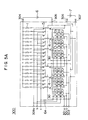
- Fig. 5A is a circuit illustration showing the switching element type recording head according to the invention, in which 301a, b to 307 denote terminals for recording operation.
- the recording head shown in Fig. 5A operates to apply a next one-line recording signal to the terminal 301 a during a period of actuating the one-line heating elements, sequentially transfer the recording signal through the eighteen shift register circuits 11 in response to a clock signal applied on the terminal 301 b, temporarily store the recording signal in the eighteen latch circuits 12 in response to a latch signal applied to the terminal 301, and switch on and off the six transistors 5 by sequentially applying signals for selecting the divisional recording heating elements to the three terminals 308a, b and c. Based on the operation, the recording head performs the three divisional recordings for finishing the recording shown in Fig. 2A.
- the terminals 308a, b, c shown in Fig. 5A are arranged to have two functions of
- a resistor 6R is provided for adjusting a voltage level of a gate signal used for synchronization for the above common connection.
- a recording head having each terminal for two functions it is possible to have the longer time of selecting each group than time of heating elements for actuation > pulse duration time of a gate signal. It is possible to actuate such a particular heating as having overlapped heating times between groups of heating elements.
- 304 and 305 denote terminals led to a power source for actuating the heating elements
- 306 and 307 denote terminals for a semiconductor IC power source.
- the manufacture process of the recording head shown in Fig. 5A includes steps of;
- the step (a) by using the output resistors of the field-effect transistors as the heating elements it is possible to further simplify the manufacture process of the recording head.
- This method makes possible to (1) remove the step of forming the resistive elements as the conventional heating elements. And, if the output resistors of the field-effect transistors are made to serve as the heating elements, it is conventionally necessary to reduce the output resistance of each field-effect transistor to 1/10 or less of the conventional heating element resistance in order to suppress unnecessary power consumption.
- Fig. 5B shows the appearance of the semiconductor IC in which the output resistances of the field-effect transistors are used as the heating elements and the semiconductor ICs are mounted by the TAB (Tape-Automated-Bonding) system.
- Fig. 5B shows the appearance of a recording head 300 A in which the semiconductor ICs are mounted by the TAB system, wherein 8 designates a silicon chip in which semiconductor ICs are mounted, 40 a head base made of metal, 50 a substrate on which heating elements are mounted, and 60 a multilayer wiring printed board.
- TFT field effect transistor
- 308a, 308b, 308c three leads for divisional recording signals of the heating elements, each lead of which is commonly connected to every two other terminals for switching signals to the field-effect transistors.
- the common electrode lead 2 and the individual electrode leads 3 formed above the three leads 308a, b, c are electrically insulated by the thin film 70 made of the two layers of the dielectric layer and the amorphous silicon layer.
- three field-effect transistors are denoted by 5, and also a wear-resisting layer for protecting them from contact wear with the thermal recording paper is not shown.
- Substrate 50 for the heating elements and the multilayer wiring printed substrate 60 are supported on the metallic head base 40.
- a group of recording head terminals 300T such as terminals for applying recording signals to the semiconductor ICs, power source terminals, and leads which collect the power terminals for actuating the heating elements are formed on substrate 60.
- the silicon chip 8 containing the semiconductor ICs 30 has the transistor terminals and the operation terminals of the semiconductor ICs connected to groups of straight leads 8a and L-character like leads 8b, respectively.
- the straight and L-like leads are supported on a film 8a and 8b made of polyimide resin by a TAB technique.
- One ends of straight and L-like leads are connected to silicon chips by ILB (Inner-Lead-Bonding).
- ILB Inner-Lead-Bonding
- the recording head according to the invention can be manufactured by the prior art except the field-effect transistor.
- the recording head with the wire-bonding technique, which is the most frequently used mounting technique of the semiconductor IC, and the other mounting technique.
- the present invention carries out the one-line recording by repeating a recording operation "n" times, wherein "n” indicates the number of the divisional recordings so named in the foregoing description, so the repeated operation is done by one n th of the heating elements (1/divisional number of recordings).
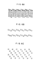
- Figs. 6A to 6C show three recording patterns according to the invention. In these Figures, one square corresponds to one recording dot.
- Fig. 6A is a view showing how the recording dots are distributed in the usual (most precise) recording. As described with reference to Fig. 2A, the usual recording system according to this invention repeats the recording operation for a first one line in the order of numbers indicated in the square shown in Fig. 6A.
- the conventional recording head carries out one line recording by every group of the heating elements grouped by the number (n) divisional recording times in accordance with the order of the arranged heating elements.
- the conventional head employs a simplified recording method of repeating a recording operation of representing recording information of two or more lines by one-line recording in the feeding direction of the recording paper.
- Fig. 6B shows recording dots corresponding to a first and a fourth lines in the distribution of dots arranged in a conventional simplified recording method, wherein recording information for three lines is represented by one-line recording for reducing the recording time into 1/3.
- the present invention can implement a simplified recording method which the conventional division recording method has been unable to meet.
- the distribution of the recording dots arranged in the simple field recording method is shown in Fig. 6C.
- Fig. 6C shows a recording pattern by which the recordings for a first line, a second line, and a third line are respectively represented by the first, the second, and the third divisional recording in order to reduce the recording time into 1/9.
- the recording dots for the first to the sixth lines are shown in this Figure.
- the simplified recording method illustrated in Fig. 6C has a feature of uniformly simplifying the information given in the main scanning direction (arranging direction of the heating elements) and sub scanning direction (feeding direction of a recording paper). For example, using the four-divisional recording head of 16 dots/mm, this method can carry out the three types of recording of 4, 8, 16 dots/mm.
- the conventional divisional recording method serves to reduce the recording time merely by reducing a recording density in the sub scanning direction. Hence, the reduction of the recording time into 1/16 results in impractically deteriorating the recording quality.
- the present simplified recording of 4 dots/mm with the 16 dots/mm head to prevent the overall density or concentration of recorded picture from being lowered, it is sufficient to increase the recording energy per dot for enlarging a recording dot size, in order to realize a practical recording.
- the simplification recording system is a useful system in facsimile transmission for a short time or test printing done by a color printer employing a high-density recording head.
- the present invention employs a new simplification recording system in which the heating elements ranged in one line are divided into a plurality of groups, each of which does not contain the adjacent heating elements, and the groups are repetitively heated one by one for recording.
- the present invention is useful of development of the future thermal recording system and is of great value in an industrial field.
Landscapes
- Electronic Switches (AREA)
Abstract
Description
- The present invention relates to a method for arranging a higher density and less cost thermal- recording head.
- The thermal recording system includes a recording unit operated in a serial printer or line printer mode.
- The serial-printer-mode recording unit employs a recording head consisting of at most one hundred heating elements. The line-printer-mode recording unit, on the other hand, requires a recording head consisting of several thousands of heating resistive elements ranged in a line. In order to heat such a great number of heating elements in response to a recording signal, the following types of recording heads were developed;
1. Diode Matrix Type - At a first phase, this type of recording head has been employed in a facsimile. It results in giving an opportunity of developing a thermal recording system. The diode matrix type recording head is designed to use a group of 32 to 64 heating elements as a single unit for recording. It thus takes several hundred mm seconds in recording one line. For reducing the recording time of one line to several mm seconds by concurrently heating many heating elements, developed are: 2. Thyristor Alloy Type and 3. Semiconductor IC Mount Type. Today, the thermal recording system normally employs a semiconductor IC mount type for thermal printing.
- In accompanying with the improvement of the recording heads, relevant matters have been also developed such as arrangements of a recording unit including how to contact a recording paper with a head and send a recording paper, improvement of coloring type thermal recording paper and development of transfer type recording paper. These developments result in that the thermal recording system is recognized as being easily handled and maintained and becomes popular in the market. The system thus applies to various kinds of fields such as:
- (a) Facsimile using coloring type thermal paper and some kinds of printers; and
- (b) Monotone printer, and multi-color or full-color printer using heat fusion type or sublimation type imprint paper, image-receiving paper.
- Figs. 1A to 1D show circuit arrangement of a recording pattern, arrangement of a heating section and an overall recording head used in a conventional semiconductor IC mount type recording head.
- Fig. 1A shows a recording pattern used in the conventional recording head, wherein 18 resistive segments ranged in a line are divided in three groups for recording. In this Figure, one square corresponds to one recording dot and a numeral shown in the square indicates how to divide the heating segments for actuating them and a heating (= recording) order.
- The conventional semiconductor IC mount type recording head, as shown in Fig. 1A, is designed to divide the eighteen resistive segments into three groups, each of which is a single recording unit consisting of adjacent six segments. Since the eighteen heating elements are ranged exactly in a line, the divisional recording system slightly shifts recording positions of second and third recorded dots relative to the recording position of the first recorded dots in the feeding direction of the recording paper.
- Fig. 1 B shows arrangement of the heating unit of the conventional semiconductor IC mount type recording head.
- In Fig. 1 B, the numerals denote these portions or elements;
- 100: Overall arrangement of the heating unit of the conventional recording head
- 1: Heating element
- 2: Common electrode
- 3: Individual electrode
- 4: Transistor
- 6: Power source for energizing heating elements
- 20: Semiconductor IC
- As shown in Fig. 1 B, the heating unit of the conventional IC-type head is configured to connect a collector of each
semiconductor IC transistor 4 to one end of each of the heating elements 1 ranged in a line, connect the other end of each heating elements 1 and an emitter of eachtransistor 4 to apower source 6 for actuating the heating elements and actuate each of N groups composed of all the heating elements in the ranging order for recording. That is, in Fig. 1 B, at first, recording signals are applied to thesemiconductor ICs 20 so as to switch on thetransistors 4 connected to the first to sixth heating elements 1 as viewed from the right. Next, by the succeeding operation, the seventh to twelfth and the thirteenth to eighteenth heating elements are actuated (heated). These operations result in providing a divisional recording pattern for one line of N = 3 as shown in Fig. 1A. - Fig. 1 C shows an example of overall circuit illustrating the conventional IC-type head, wherein;
- 101: Conventional IC-type recording head circuit
- 7: Power source for semiconductor IC
- 20: Conventional semiconductor IC circuit
- The
IC circuit 20 comparises; - 11: shift register for transferring a recording signal
- 12: latch circuit for temporarily storing a recording signal
- 13: gate circuit for supplying a recording signal of a latch circuit
- 4: transistor for supplying a recording output (actuating a heating element)
- The terminals of the
semiconductor IC 20 are respectively connected to the eighteen elements 1 as shown for forming recording head actuating terminals 101 a, c to 107. - The
terminals - The recording head is designed to apply a one-line recording signal to the terminal 101a, transfer the recording signal sequentially through the eighteen shift register circuits 11 in response to a clock signal from the
terminal 101b, and temporarily store the recording signal transferred by a latch signal from theterminal 102 in the eighteenlatch circuits 12. - In response to a gate signal applied to the terminal 103, the first to
sixth transistors 4 as viewed from the right hand become conductive in response to the recording signals stored in the corresponding latch circuits. Then, the six heating elements 1 connected to theconductive transistors 4 are heated up by thepower source 6 for actuating the heating elements, the power source being connected to theterminals - During a period of recording one line, the next line signal is applied to the terminal 101a a for preparing the succeeding next line recording. Likewise, the subsequent lines are recorded in the divisional recording mode. In addition, 104 and 105 denote semiconductor IC power terminals of the recording head. The foregoing three types of recording heads;
- 1. Diode Matrix Type
- 2. Thyristor Array Type
- 3. Semiconductor IC Mount Type
- The shortcoming of the arrangement of the heating unit shown in Fig.1 B is to require connection of heating resistive elements to semiconductor devices (diode array, thyristor array or output transistor array) in one-to-one relationship by a high density lead line pattern. That is, the manufacture of a heating element actuating type recording head as shown in Fig. 1B becomes more difficult as the array density of the heating elements becomes higher.
- Because of the above reason, today,
- (1) the high-density thermal recording head has a limitation to array density, that is, 16 dots per millimeter. To solve the shortcoming, the simultaneous formation of the heating elements and the semiconductor IC devices is being developed using a thin film forming technique but is not still put into practice; and
- (2) the connection between the heating elements and the semiconductor devices with a high-density lead line makes it difficult to lower the manufacturing cost of semiconductor IC-type head by the conventional manufacturing technique.
- The present invention is implemented for the main purposes of:
- (1) realization of a high-density recording head, and
- (2) reduction of the cost of the recording head, by lessening the quantity of semiconductor devices required for the recording head and lowering a density of connection between the heating elements and the semiconductor devices.
- It is therefore a first object of the present invention to provide a high-density thermal recording head which has a density of 16 or more dots per millimeter and can be produced by the conventional head manufacturing technique.
- It is a second object of the present invention to reduce the manufacturing cost of the head with a density of 6 to 12 dots per millimeter which is most frequently used.
- It is a third object of the present invention to provide a recording system operable with a reduced recording time by using a more coarse recording density than an array density of the heating elements by virtue of a recording head provided according to the invention.
- To achieve the foregoing objects, the present invention employs a novel divisional recording system of heating elements. That is, the invention comprises;
- (1) means for selecting a heating element one by one from among adjacent N heating elements and dividing all the heating elements into N groups, and
- (2) means for simultaneously heating selected one element of all the groups, whereby the heating elements arranged in one line are divided into N groups for recording.
-
- Figs. 1A to 1D are views illustrating a conventional thermal recording system, wherein Figs. 1A shows a recording pattern used in a conventional divisional recording system,
- Fig. 1 B arrangement of a heating unit used in the conventional recording head,
- Fig. 1 C a conventional semiconductor IC-type head circuit, and
- Fig. 1 D a heating unit of a switching element type recording head employing the conventional divisional recording system,
- Fig. 2 are views illustrating a thermal recording system according to the invention, wherein Fig. 2A shows a recording pattern used in a divisional recording system according to the invention,
- Fig. 2B shows arrangement of a heating unit used in a common electrode divisional type recording head according to the invention, and
- Fig. 2C shows arrangement of a heating unit used in a switching element type recording head according to the invention;
- Fig. 3 is a view illustrating arrangement of a semiconductor IC;
- Fig. 4 are views illustrating a concrete example of a common electrode divisional system recording head according to the invention; wherein Fig. 4A shows a common electrode divisional system circuit,
- Fig. 4B shows a circuit showing the appearance of a common electrode divisional system recording head having a semiconductor IC mounted by a wire-bonding technique;
- Fig. 5 are views illustrating a concrete example of a switching element system recording head according to the invention, wherein
- Fig. 5A shows a switching element system circuit,
- Fig. 5B shows appearance of a switching element system recording head having a mounted semiconductor IC with a TAB system; and
- Fig. 6 are views illustrating how to improve a recording speed by setting a more coarse recording density of the heating elements in the arranging direction according to the invention, wherein
- Fig. 6A shows a recording pattern for normal recording,
- Fig. 6B shows a recording pattern formed on the conventional simplification recording system using a recording head formed according to the invention, and
- Fig. 6C shows a recording pattern used according to a new simple recording method of the invention.
- Fig. 2A shows a one-line recording pattern formed in the case where a divisional recording system of the invention performs recording by dividing eighteen resistors ranged in a line into three groups. The way of illustration of Fig. 2A is similar to that in Fig. 1A.
- For recording one line, the present invention is designed to actuate, at first, a first group of the first, 4-th, 7-th, 10-th, 13-th and 16-th resistors for recording the corresponding dots as viewed from the left hand and then repeat the similar divisional recording twice.
- Since one line is recorded in the foregoing order of the resistors, the present recording system is more likely to shift the recording dots out of proper positions than the conventional recording system. This shortcoming can be prevented by shifting the heating element arrangement in the travelling direction of the recording paper.
- Figs. 2B and 2C show arrangements of two heating units according to the present invention for performing the divisional recording described with reference to Fig. 2A.
- Fig. 2B shows a
heating unit 200 employing a common electrode divisional system according to the invention. This heating unit comprises heating elements 1 ranged in one line, - (1) three
common electrodes 206a, b, c, each of which is commonly connected to the terminals of the heating elements selected respectively from each group consisting of adjacent three heating elements, and - (2) a plurality of individual terminals commonly connected to the other terminals of the adjacent N heating elements.
This recording head has aswitch circuit 6s for switching aheating power source 6. For performing the recording described with reference to Fig. 2(a), the recording head operates the switch to - (3) connect the
power source 6 for actuating the heating elements to three common electrodes 204a, b, c sequentially, and - (4) switch on or off the transistors connected to each
individual terminal 3 in synchronization with the operation of (3) in response to a recording signal. - Fig. 2C shows a
heating unit 300 employing a switching element system according to the invention. The heating unit comprises a plurality of heating elements 1 and switching elements 5 (for example, field-effect transistors) ranged in one line, - (1) a
common terminal 306 commonly connected to the terminals of the heating elements 1, - (2) a plurality of
individual terminals 3 connecting the other terminals of the heating elements 1 to the terminals of theswitching elements 5 and commonly connecting the other terminals of the adjacent three switching elements with one another, and - (3) divisional recording
signal input terminals 303a, b, c, each of which is commonly connected to the switching signal terminals of switchingelements 5 each selected sequentially respectively from each group consisting of threeadjacent switching elements 5. For performing the recording described with reference to Fig. 2A, this type recording head operates to; - (4) connect the
power source 6 for actuating the heating elements to thecommon terminal 306, and - (5) sequentially select a group of heating elements in response to a divisional recording signal serially applied to the three
switching terminals 303a, b, c and switch on and off the transistors mounted on the semiconductor IC connected to theindividual electrodes 3 in response to a recording signal synchronized with the divisional recording signal. - As will be understood from the foregoing description of Fig. 1 C, it is necessary to provide the same number of
transistors 4 mounted on the semiconductor IC as the heating elements for fabricating the conventional IC-type recording head. - On the contrary, the present invention reduces the number of
transistors 4 mounted therein to 1/divisional number of recordings. - As such, this invention reduces the number of transistors included therein more greatly than the conventional recording head arrangement. It is thus possible to achieve the main purposes of the invention, that is, high recording density and less costly recording head.
- As described above, the thermal recording system mainly employ an IC type recording head, because a one-line recording time is shortered as
one-line recording time = divisional number of recordings x (multiplied by) width of a pulse for actuating the heating elements....(1) - The above equation has no concern with the sum of the heating elements included in the recording head.
- Hence, though it is impractical to increase the divisional number of recordings too much. But, for making sure of uniform recording quality and assurance of the heating elements-life the divisional recordings of the relation N = 3 to 5
is necessary to cool the heating element during a triple to fivefold period of a pulse width for actuating the heating elements. Hence, as a design of a concrete recording head, assuming that divisional number of recordings N = 4 leading wires between heating elements and semiconductor ICs = 8 per millimeter, the conventional manufacturing technique makes it possible to manufacture the recording head ar
ranged to have 32 dots/mm as shown in Fig. 2B. - For manufacturing the most frequently used recording head arranged to have 8 to 12 dots/mm, the recording head is made less costly by reducing to 1/N
- (1) the number of semiconductor ICs
- (2) leading wires connecting between heating elements and semiconductor ICs.
- For reference, Fig. 1D shows arrangement of a switching element system heating unit employing the conventional divisional recording system. The function of each terminal is similar to that shown in Fig. 2B. Thus, these terminals referenced by like numerals are not explained.
- As will be understood from Fig. 1 D, the conventional divisional recording system for the heating elements is designed to disperse to various locations the heating elements are connected to the
individual terminals 3 on the overall width. Hence, as the heating members become more, the connection of a leading wire for forming individual terminals is made surprisingly more complicated. It is a great obstacle to the arrangement of a concrete head. - It should be noted that the divisional recording system of the invention described with reference to Fig. 2A is an indispensable method for reducing the number of semiconductor ICs and leading wires of the semiconductor ICs.
- The recording head of the invention may be arranged by the
conventional semiconductor IC 20. This recording head, however, requires the change of a transferring order of a recording signal outside of itself. - Fig. 3 is a circuit diagram of a semiconductor IC according to the present invention. The semiconductor IC is arranged to change the order of a recording signal for the conventional recording head inside of it and actuate the heating elements in the order shown in Fig. 2B. Fig. 3 shows a circuit diagram showing an
overall semiconductor IC 30 according to the invention. Like the conventional semiconductor IC, this semiconductor IC comprises - 11: shift registers for transferring recording signals,
- 12: latch circuits for temporarily saving the recording signals,
- 13: gate circuits for outputting the recording signals of the latch circuits, and
- 4: transistors for outputting the recording signals (actuating the heating elements).
- The semiconductor IC has three functions of:
- (1) applying a next one-line recording signal to a terminal 31 a during a period of heating one-line heating elements, sequentially transferring the recording signals through nine shift register circuits 11 in response to a clock signal applied on a terminal 31c, and outputting the recording signals to the terminal 31 b,
- (2) temporarily storing the recording signals in nine
latch circuits 12 in response to a latch signal applied on the terminal 32a, - (3) outputting to three
transistors 4 the recording signals of- 1 st, 4th, 7th, 10th, 13th, 16th
- 2nd, 5th, 8th, 11 th, 14th, 17th
- 3rd, 6th, 9th, 12th, 15th, 18th
- The
semiconductor IC 30 has a somewhat enlarged chip size because of a large number of circuits (shiftregister 11,latch 12 and gate 13), though, it is still practical in that; - (a) the chip size is not increased so much since the
transistor 4 occupies large area, and - (b) the recording head requires only 1/N semiconductor ICs.
- The present embodiment describes the common electrode division type head according to the invention. The recording head mounts the
semiconductor ICs 30 by wire-bonding technique. - Fig. 4A is a circuit illustration showing a common electrode
division type head 200 employing thesemiconductor ICs 30 according to the invention. In this circuit, the terminals of thesemiconductor ICs 30 are respectively connected to eighteen resistors 1 for forming recording operation terminals 201 a, c to 207. - The recording head shown in Fig. 4A operates to;
- (1) apply a next one-line recording signal to the terminal 201 a during a period of actuating one-line heating elements and sequentially transfer the recording signals to eighteen shift register circuits 11 in response to the clock signal applied on the terminal 201 b,
- (2) temporarily store the recording signals in eighteen
latch circuits 12 in response to the latch signal applied to the terminal 202, - (3) sequentially connect the terminals 204a, b, c to a power source for actuating the heating elements with a
switching circuit 6s, and - (4) switch on and off six
transistors 4 in response to a gate signal applied to thegate circuit 12 with the switching operation and simultaneously actuate each group of the heating elements 1 of;- 1 st, 4th, 7th, 10th, 13th, 16th
- 2nd, 5th, 8th, 11 th, 14th, 17th
- 3rd, 6th, 9th, 12th, 15th, 18th
- Having the
switching circuit 6s, the recording head shown in Fig. 4A is arranged to synchronize the switching connection of the terminals 204a, b, c to the power source and the switching operation of the gate signal by the connection of the three common electrodes 204a, b, c respectively to thegate signal terminals 33a, b, c. 6R denotes a resistor, which serves to adjust a voltage level of the gate signal for the synchronization by the above connection. Further, 205 denotes a terminal led to the power source for actuating the heating elements. 206 and 207 each denotes a terminal led to a semiconductor IC power source. - As will be understood from the above explanation, the recording head of this embodiment can be operated similarly with the conventional semiconductor IC type recording head by the same recording signal as conventional IC-type head.
- Fig. 4B shows the concrete structure of the
recording head 200 having semiconductor ICs mounted by a wire-bonding technique. - In Fig. 4B, 200A is a view showing an overall recording head and 200T is a view showing a group of terminals provided in the recording head, wherein
- 1: heating elements ranged in one line,
- 2a: a common electrode lead of the heating elements,
- 2b: wiring conductors for forming common electrodes of the heating elements,
- 3a: individual electrode leads for the heating elements,
- 3b, 3c: wiring conductors for forming a multilayer wiring portion of terminals for driving the semiconductor ICs,
- 50: substrate on which the heating elements are mounted,
- 51: thermal and electric insulating layer, and
- 8: silicon chip of semiconductor IC circuit.
- The recording head shown in Fig. 4B comprises a
substrate 50 on which a thermal and electric insulating layer 51 (for example, a glass layer of about 20 microns) is formed. A layer of the heating elements, and a layer of common electrode and individual electrode lead are formed on the thermal and electric insulatinglayer 51 by a thin film forming technique. A patterning technique is applied to form the heating elements 1 ranged in one line, common electrode leads 2a of the heating elements, individual electrode leads 3a of the heating elements and multilayer wiring leads 3b. - Between the
substrate 50 and the thermal and electric insulatingglass layer 51 are formed threeconductors 2b serving as the common electrodes for the heating elements. Eachcommon electrode lead 2a is connected to the correspondingconductor 2b every two other leads via respective throughhole 51 a formed in the glass layer. - Every three individual electrode leads 3a of the heating elements are patterned to be electrically in unit, and the end portion of
leads 3a are connected to each transistor formed in the semiconductor IC. - Wiring leads 3b are formed by patterning simultaneous with the patterning of the electrode leads 2a and 2b formed with a spacing slightly longer than the length of the IC from the connecting portion of the transistor and serve to collect the driving terminals of the semiconductor ICs in order to forming a main terminal of the recording head. The wiring leads 3b are electrically connected to the
wiring conductors 3c of the operating terminal of the recording head via respective through holes 51 b. - A
semiconductor silicon chip 8 is bonded in a space between the individual electrode leads 3a and the wiring leads 3b. And, by wire-bonding technique,gold wires 9 are connected between theindividual electrodes 3a of the heating elements and the pad portions of the transistors of each semiconductor IC and also between the pad portions of the driving terminals of the semiconductor IC and the wiring leads 3b. Thus finished is the electric circuit connection of the main portion shown in Fig. 4B except connection between 33a, b, c and 204a, b, c. - Further, though not shown, with the process for forming the heating elements, it may be possible to form a
resistor 6R for adjusting a voltage level of the gate signal shown in Fig. 5B on thesubstrate 50 on which the heating elements are mounted. - Moreover, for simplifying the manufacture process and reducing the manufacture cost, the structure of the recording head may have the improved features of
- 1. making it easy to form the high density through-
holes 51 a and 51 b by forming the layer of glass beneath the resistive elements 1 and the layer of polyimidefilm beneath theleads - 2. changing the pattern shape form of the conducting layer for forming the multi layer wiring portion of the semiconductor IC, which connects from the
terminal group 200T of the recording head to a connector through a flexible film, and - 3. commonly connecting the
common electrode 2a of the heating elements to the respective lead for a gate signal in order to reduce the number of leads contained in the recording head. - Further, with reference to the present embodiment, it is possible to manufacture a recording head using another semiconductor IC mounting technique.
- This embodiment is of a switching element type recording head on which the semiconductor ICs are mounted by a TAB (Tape-Automated-Bonding) system.
- Fig. 5A is a circuit illustration showing the switching element type recording head according to the invention, in which 301a, b to 307 denote terminals for recording operation.
- The recording head shown in Fig. 5A operates to apply a next one-line recording signal to the terminal 301 a during a period of actuating the one-line heating elements, sequentially transfer the recording signal through the eighteen shift register circuits 11 in response to a clock signal applied on the terminal 301 b, temporarily store the recording signal in the eighteen
latch circuits 12 in response to a latch signal applied to the terminal 301, and switch on and off the sixtransistors 5 by sequentially applying signals for selecting the divisional recording heating elements to the threeterminals 308a, b and c. Based on the operation, the recording head performs the three divisional recordings for finishing the recording shown in Fig. 2A. - The
terminals 308a, b, c shown in Fig. 5A are arranged to have two functions of - 1) selecting the divisional recording heating elements, and
- 2) outputting the recording signal stored in the latch circuit.
- A
resistor 6R is provided for adjusting a voltage level of a gate signal used for synchronization for the above common connection. - If the difference between the switching characteristics of the
transistor 4 and theswitching element 5 is a serious matter, it is possible to form separate circuit terminals for the two functions respectively. - In a recording head having each terminal for two functions, it is possible to have the longer time of selecting each group than time of heating elements for actuation > pulse duration time of a gate signal. It is possible to actuate such a particular heating as having overlapped heating times between groups of heating elements. In addition, 304 and 305 denote terminals led to a power source for actuating the heating elements, 306 and 307 denote terminals for a semiconductor IC power source.
- The manufacture process of the recording head shown in Fig. 5A includes steps of;
- (a) producing the heating elements and field-effect transistors formed of amorphous silicon thin film by a thin film forming technique and producing a high-density circuit connections as shown in Fig. 2C, and
- (b) electrically connecting the field-effect transistors with the semiconductor IC by the conventional mounting technique.
- Further, at the step (a), by using the output resistors of the field-effect transistors as the heating elements it is possible to further simplify the manufacture process of the recording head. This method makes possible to (1) remove the step of forming the resistive elements as the conventional heating elements. And, if the output resistors of the field-effect transistors are made to serve as the heating elements, it is conventionally necessary to reduce the output resistance of each field-effect transistor to 1/10 or less of the conventional heating element resistance in order to suppress unnecessary power consumption. However, this present method assumes and relays on the relation (2) of the output resistance of the field-effect transistor = the heating element resistance. (That is, @ to make the output resistance = resistance of heating elements.) It results in mitigating the restriction against the output resistance of the field-effect transistor. And, these two kinds of recording heads have the same circuit arrangements.
- Fig. 5B shows the appearance of the semiconductor IC in which the output resistances of the field-effect transistors are used as the heating elements and the semiconductor ICs are mounted by the TAB (Tape-Automated-Bonding) system.
- Fig. 5B shows the appearance of a
recording head 300 A in which the semiconductor ICs are mounted by the TAB system, wherein 8 designates a silicon chip in which semiconductor ICs are mounted, 40 a head base made of metal, 50 a substrate on which heating elements are mounted, and 60 a multilayer wiring printed board. - The following processes make it possible to form field effect transistor (TFT) and three type of electrodes on the
substrate 50. - 308a, 308b, 308c: three leads for divisional recording signals of the heating elements, each lead of which is commonly connected to every two other terminals for switching signals to the field-effect transistors.
- 70: thin film formed of two layers, that is, a dielectric layer and an amorphous silicon layer,
- 2: a single common electrode lead connecting drain electrodes and drains of the field-effect transistors,
- 3: a plurality of individual electrode leads connected to the source terminals of the respective adjacent three field-effect transistors. The
common electrode lead 2 and the individual electrode leads 3 formed above the threeleads 308a, b, c are electrically insulated by thethin film 70 made of the two layers of the dielectric layer and the amorphous silicon layer. For easier understanding of the figure, three field-effect transistors are denoted by 5, and also a wear-resisting layer for protecting them from contact wear with the thermal recording paper is not shown. -
Substrate 50 for the heating elements and the multilayer wiring printedsubstrate 60 are supported on themetallic head base 40. A group ofrecording head terminals 300T such as terminals for applying recording signals to the semiconductor ICs, power source terminals, and leads which collect the power terminals for actuating the heating elements are formed onsubstrate 60. - The
silicon chip 8 containing thesemiconductor ICs 30 has the transistor terminals and the operation terminals of the semiconductor ICs connected to groups ofstraight leads 8a and L-character likeleads 8b, respectively. The straight and L-like leads are supported on afilm like lead group - (1) a plurality of individual electrode leads 3 connected to the source terminals of the field-effect transistor, and
- (2) a group of leads forming the
recording head terminals 300T, which are respectively formed by the TAB type OLB technique (Outer-Lead-Bonding). Further, with fourleads 8c supported by thepolyimide resin film 8e, - (3) a
common electrode lead 2 connected to the drains of the field-effect transistors, and - (4) three
switching signal terminals 308a, b, c of the field-effect transistors are connected to the group ofleads 300T. Thus completed is the electric circuit connection of the recording head shown in Fig. 5A. - As will be understood from the above description, the recording head according to the invention can be manufactured by the prior art except the field-effect transistor.
- With reference to this embodiment, it is possible to manufacture the recording head with the wire-bonding technique, which is the most frequently used mounting technique of the semiconductor IC, and the other mounting technique.
- (Embodiment 3) How to shorten a recording time by setting a more coarse or lower recording density in the arranging direction of the heating elements is next explained.
- In the normal or usual recording, the present invention carries out the one-line recording by repeating a recording operation "n" times, wherein "n" indicates the number of the divisional recordings so named in the foregoing description, so the repeated operation is done by one n th of the heating elements (1/divisional number of recordings).
- This divisional recording system can realize a new simplified recording for increasing the recording speed by the setting of;
one-line recording = one division recording - Figs. 6A to 6C show three recording patterns according to the invention. In these Figures, one square corresponds to one recording dot.
- Fig. 6A is a view showing how the recording dots are distributed in the usual (most precise) recording. As described with reference to Fig. 2A, the usual recording system according to this invention repeats the recording operation for a first one line in the order of numbers indicated in the square shown in Fig. 6A.
- The conventional recording head carries out one line recording by every group of the heating elements grouped by the number (n) divisional recording times in accordance with the order of the arranged heating elements. For improving the recording speed, therefore, the conventional head employs a simplified recording method of repeating a recording operation of representing recording information of two or more lines by one-line recording in the feeding direction of the recording paper.
- Fig. 6B shows recording dots corresponding to a first and a fourth lines in the distribution of dots arranged in a conventional simplified recording method, wherein recording information for three lines is represented by one-line recording for reducing the recording time into 1/3.
- The present invention can implement a simplified recording method which the conventional division recording method has been unable to meet. The distribution of the recording dots arranged in the simple field recording method is shown in Fig. 6C.
- Fig. 6C shows a recording pattern by which the recordings for a first line, a second line, and a third line are respectively represented by the first, the second, and the third divisional recording in order to reduce the recording time into 1/9. The recording dots for the first to the sixth lines are shown in this Figure.
- The simplified recording method illustrated in Fig. 6C has a feature of uniformly simplifying the information given in the main scanning direction (arranging direction of the heating elements) and sub scanning direction (feeding direction of a recording paper). For example, using the four-divisional recording head of 16 dots/mm, this method can carry out the three types of recording of 4, 8, 16 dots/mm.
- This method has another feature that the recording time can be reduced into for 8 dots/mm, 1/2x1/2 = 1/4; and for 4 dots/mm, 1/4 x 1/4 = 1/16.
- The conventional divisional recording method serves to reduce the recording time merely by reducing a recording density in the sub scanning direction. Hence, the reduction of the recording time into 1/16 results in impractically deteriorating the recording quality. On the other hand, in the case of the present simplified recording of 4 dots/mm with the 16 dots/mm head, to prevent the overall density or concentration of recorded picture from being lowered, it is sufficient to increase the recording energy per dot for enlarging a recording dot size, in order to realize a practical recording.
- The simplification recording system is a useful system in facsimile transmission for a short time or test printing done by a color printer employing a high-density recording head.
- As described above, the present invention employs a new simplification recording system in which the heating elements ranged in one line are divided into a plurality of groups, each of which does not contain the adjacent heating elements, and the groups are repetitively heated one by one for recording. Hence, the invention makes it possible to
- (1) reduce the number of semiconductor ICs serving to selectively heat the heating elements and the density of the connection between the heating elements and the leads, and manufacture a high-density recording head of 16 dots/mm or more which it has been difficult for the prior art to manufacture, and
- (2) reduce the number of semiconductor ICs mounted in the overall recording head and lower the cost of the recording head. Hence, the present system offers some effects of
- (3) providing the arrangements of two concrete recording heads, that is, the common electrode division system and the switching element system,
- (4) illustrating the arrangement of a semiconductor IC which makes it possible to change the inputting order of the recording signals to the proper recording order for the divisional recording system according to the invention,
- (5) offering a new simplification recording system for reducing a recording time by setting a more coarse density than the array density of the heating elements.
- These effects make great contributions to improvement of the related arts about the thermal recording system. The present invention is useful of development of the future thermal recording system and is of great value in an industrial field.
have respective circuit arrangements according to the semiconductor devices connected to the heating elements. However, the feature of deviding the heating elements for one line recording as in Figs. 1A and B is common to these three heads.
in response to the gate signals applied on the
for continuously performing the divisional recording of each line. The above ordinal numbers are counted from the right hand.
In addition, for easier understanding of the figure, there is not shown a wear-resisting layer on the heating element for preventing contact wear with a thermal recording paper.
Claims (7)
further,
Priority Applications (1)
| Application Number | Priority Date | Filing Date | Title |
|---|---|---|---|
| DE69017016T DE69017016T2 (en) | 1990-07-20 | 1990-07-20 | Thermal printing system and thermal print head. |
Applications Claiming Priority (1)
| Application Number | Priority Date | Filing Date | Title |
|---|---|---|---|
| US07/553,421 US5075701A (en) | 1990-07-17 | 1990-07-17 | Thermal recording head having group-wise actuable heating elements |
Publications (2)
| Publication Number | Publication Date |
|---|---|
| EP0466968A1 true EP0466968A1 (en) | 1992-01-22 |
| EP0466968B1 EP0466968B1 (en) | 1995-02-15 |
Family
ID=24209329
Family Applications (1)
| Application Number | Title | Priority Date | Filing Date |
|---|---|---|---|
| EP90113981A Expired - Lifetime EP0466968B1 (en) | 1990-07-17 | 1990-07-20 | Thermal recording system and thermal recording head |
Country Status (2)
| Country | Link |
|---|---|
| US (1) | US5075701A (en) |
| EP (1) | EP0466968B1 (en) |
Families Citing this family (9)
| Publication number | Priority date | Publication date | Assignee | Title |
|---|---|---|---|---|
| US6106102A (en) * | 1992-05-01 | 2000-08-22 | Hewlett-Packard Company | Odd number of passes, odd number of advances, and separated-diagonal-line masking, in liquid-ink printers |
| DE4221963C2 (en) * | 1992-06-30 | 1995-10-05 | Eastman Kodak Co | Method of recording information |
| JP3305115B2 (en) * | 1994-06-01 | 2002-07-22 | キヤノン株式会社 | Recording apparatus and method, recording head and driving circuit thereof |
| US5754193A (en) * | 1995-01-09 | 1998-05-19 | Xerox Corporation | Thermal ink jet printhead with reduced power bus voltage drop differential |
| US6195110B1 (en) * | 1997-07-28 | 2001-02-27 | Fuji Photo Film Co., Ltd. | Thermal printing method and apparatus having groups of separately drive heating elements in the thermal head |
| JP2001232841A (en) * | 2000-02-21 | 2001-08-28 | Alps Electric Co Ltd | Method for controlling energization of line thermal head |
| KR100788658B1 (en) * | 2004-12-15 | 2007-12-26 | 삼성전자주식회사 | Method for driving thermal head and image forming device employing the same |
| US8080731B2 (en) * | 2007-06-15 | 2011-12-20 | The Boeing Company | Restrained solar collector and method |
| JP6384080B2 (en) * | 2014-03-25 | 2018-09-05 | セイコーエプソン株式会社 | Liquid ejecting apparatus and method for controlling liquid ejecting apparatus |
Citations (2)
| Publication number | Priority date | Publication date | Assignee | Title |
|---|---|---|---|---|
| US4395146A (en) * | 1980-11-06 | 1983-07-26 | Sony Corporation | Method and apparatus for operating a thermal printer with uniform heat distribution |
| US4492482A (en) * | 1982-01-25 | 1985-01-08 | Sony Corporation | Thermal head driving system |
Family Cites Families (6)
| Publication number | Priority date | Publication date | Assignee | Title |
|---|---|---|---|---|
| JPS533246A (en) * | 1976-06-29 | 1978-01-12 | Matsushita Electric Ind Co Ltd | Thermal recording head |
| JPS6079977A (en) * | 1983-10-07 | 1985-05-07 | Fuji Xerox Co Ltd | Driving system for thermal head |
| JPS60190367A (en) * | 1984-03-12 | 1985-09-27 | Hitachi Ltd | Construction of thermal head |
| US4779102A (en) * | 1985-12-05 | 1988-10-18 | Ricoh Company, Ltd. | Head drive system for a thermal printer |
| JPS63173660A (en) * | 1987-01-14 | 1988-07-18 | Sanyo Electric Co Ltd | Driving circuit for thermal head |
| JPS63216764A (en) * | 1987-03-06 | 1988-09-09 | Mitsubishi Electric Corp | Recording method by thermal head |
-
1990
- 1990-07-17 US US07/553,421 patent/US5075701A/en not_active Expired - Lifetime
- 1990-07-20 EP EP90113981A patent/EP0466968B1/en not_active Expired - Lifetime
Patent Citations (2)
| Publication number | Priority date | Publication date | Assignee | Title |
|---|---|---|---|---|
| US4395146A (en) * | 1980-11-06 | 1983-07-26 | Sony Corporation | Method and apparatus for operating a thermal printer with uniform heat distribution |
| US4492482A (en) * | 1982-01-25 | 1985-01-08 | Sony Corporation | Thermal head driving system |
Non-Patent Citations (1)
| Title |
|---|
| PATENT ABSTRACTS OF JAPAN vol. 13, no. 6 (M-781)(3354) 09 January 1989, & JP-A-63 216764 (MASAYUKI SAITO ET AL) 09 September 1988, * |
Also Published As
| Publication number | Publication date |
|---|---|
| EP0466968B1 (en) | 1995-02-15 |
| US5075701A (en) | 1991-12-24 |
Similar Documents
| Publication | Publication Date | Title |
|---|---|---|
| EP0079063B1 (en) | Thermal printing head | |
| US4651164A (en) | Thermal print head | |
| EP0466968B1 (en) | Thermal recording system and thermal recording head | |
| US5786839A (en) | Electronic parts, thermal head, manufacturing method of the thermal head, and heat sensitive recording apparatus | |
| US5307089A (en) | Optical printing head | |
| JPH02235756A (en) | Recording head and substrate therefor | |
| US6611280B1 (en) | Flexible cable, flexible cable mount method, semiconductor device with flexible cable, led array head with flexible cable, image forming apparatus with such led array head | |
| US4405929A (en) | Thermal head device | |
| JPS6250313B2 (en) | ||
| KR930011865B1 (en) | Heat sensitive recording method, heat sensitive recording head and heat sensitive recording semiconductor | |
| US5729275A (en) | Thermal printhead, drive IC for the same and method for controlling the thermal printhead | |
| US4935637A (en) | Linear element array with wire bonding arrangement | |
| EP0128760A1 (en) | Thermal recording head | |
| JPS62211157A (en) | Densely packed ic-mounted type thermal head | |
| JP2734051B2 (en) | Thermal recording head | |
| JP2020179514A (en) | Driver ic for thermal print head, thermal print head and wiring pattern of thermal print head | |
| JPH0723006B2 (en) | Light emitting diode print head | |
| JPS5845974A (en) | Thermal head | |
| EP0369347B1 (en) | Thermal print head | |
| JPH0467958A (en) | Thermal recording head | |
| JPH0596766A (en) | Wiring pattern of thermal head | |
| JPH0339251Y2 (en) | ||
| JPH0737148B2 (en) | Thermal recording head | |
| KR940010877B1 (en) | Photo diode printer head | |
| JPH04132957U (en) | thermal head |
Legal Events
| Date | Code | Title | Description |
|---|---|---|---|
| PUAI | Public reference made under article 153(3) epc to a published international application that has entered the european phase |
Free format text: ORIGINAL CODE: 0009012 |
|
| 17P | Request for examination filed |
Effective date: 19901228 |
|
| AK | Designated contracting states |
Kind code of ref document: A1 Designated state(s): DE FR GB |
|
| 17Q | First examination report despatched |
Effective date: 19930928 |
|
| GRAA | (expected) grant |
Free format text: ORIGINAL CODE: 0009210 |
|
| AK | Designated contracting states |
Kind code of ref document: B1 Designated state(s): DE FR GB |
|
| REF | Corresponds to: |
Ref document number: 69017016 Country of ref document: DE Date of ref document: 19950323 |
|
| ET | Fr: translation filed | ||
| PG25 | Lapsed in a contracting state [announced via postgrant information from national office to epo] |
Ref country code: GB Effective date: 19950720 |
|
| PGFP | Annual fee paid to national office [announced via postgrant information from national office to epo] |
Ref country code: FR Payment date: 19950728 Year of fee payment: 6 |
|
| PGFP | Annual fee paid to national office [announced via postgrant information from national office to epo] |
Ref country code: DE Payment date: 19950929 Year of fee payment: 6 |
|
| PLBE | No opposition filed within time limit |
Free format text: ORIGINAL CODE: 0009261 |
|
| STAA | Information on the status of an ep patent application or granted ep patent |
Free format text: STATUS: NO OPPOSITION FILED WITHIN TIME LIMIT |
|
| 26N | No opposition filed | ||
| GBPC | Gb: european patent ceased through non-payment of renewal fee |
Effective date: 19950720 |
|
| PG25 | Lapsed in a contracting state [announced via postgrant information from national office to epo] |
Ref country code: FR Effective date: 19970328 |
|
| PG25 | Lapsed in a contracting state [announced via postgrant information from national office to epo] |
Ref country code: DE Effective date: 19970402 |
|
| REG | Reference to a national code |
Ref country code: FR Ref legal event code: ST |