EP0466934B1 - Data carrier - Google Patents
Data carrier Download PDFInfo
- Publication number
- EP0466934B1 EP0466934B1 EP91903623A EP91903623A EP0466934B1 EP 0466934 B1 EP0466934 B1 EP 0466934B1 EP 91903623 A EP91903623 A EP 91903623A EP 91903623 A EP91903623 A EP 91903623A EP 0466934 B1 EP0466934 B1 EP 0466934B1
- Authority
- EP
- European Patent Office
- Prior art keywords
- shift register
- data
- signal
- circuit
- output
- Prior art date
- Legal status (The legal status is an assumption and is not a legal conclusion. Google has not performed a legal analysis and makes no representation as to the accuracy of the status listed.)
- Expired - Lifetime
Links
Images






Classifications
-
- G—PHYSICS
- G06—COMPUTING OR CALCULATING; COUNTING
- G06K—GRAPHICAL DATA READING; PRESENTATION OF DATA; RECORD CARRIERS; HANDLING RECORD CARRIERS
- G06K19/00—Record carriers for use with machines and with at least a part designed to carry digital markings
- G06K19/06—Record carriers for use with machines and with at least a part designed to carry digital markings characterised by the kind of the digital marking, e.g. shape, nature, code
- G06K19/067—Record carriers with conductive marks, printed circuits or semiconductor circuit elements, e.g. credit or identity cards also with resonating or responding marks without active components
- G06K19/07—Record carriers with conductive marks, printed circuits or semiconductor circuit elements, e.g. credit or identity cards also with resonating or responding marks without active components with integrated circuit chips
- G06K19/0723—Record carriers with conductive marks, printed circuits or semiconductor circuit elements, e.g. credit or identity cards also with resonating or responding marks without active components with integrated circuit chips the record carrier comprising an arrangement for non-contact communication, e.g. wireless communication circuits on transponder cards, non-contact smart cards or RFIDs
-
- G—PHYSICS
- G06—COMPUTING OR CALCULATING; COUNTING
- G06K—GRAPHICAL DATA READING; PRESENTATION OF DATA; RECORD CARRIERS; HANDLING RECORD CARRIERS
- G06K7/00—Methods or arrangements for sensing record carriers, e.g. for reading patterns
- G06K7/0008—General problems related to the reading of electronic memory record carriers, independent of its reading method, e.g. power transfer
Definitions
- the present invention relates to data carriers provided for control of tools for machine tools, parts and products in a factory, or an article identification system such as a physical distribution system.
- a resonance circuit 201 is connected to a coil for reception, a signal obtained at the resonance circuit is waveform shaped in a waveform shaping circuit 202, data is written into a memory 204 through a memory control portion 203 including a gate array, a CPU and so on, or data is read out based on a command given and is supplied by absorbing the vibration of resonance circuit 201 by a vibration absorbing circuit 205.
- a data carrier employing ultrasonic wave data transmission which has a shift register for circulating and holding data obtained from an input circuit and has signal switching means for switching the input supplied to the shift register from the output of the input circuit to the output of the shift register, in response to an output of the shift register.
- JP-A-51 150 917 shows a data carrier using electromagnetic coupling and having a shift register for data storage.
- the present invention is made in view of such a problem of a conventional data carrier, and an object thereof is to make it possible to hold a small amount of data with a highly simplified structure suitable for a reduced storage capacity and to write and read data using a conventional write/read control unit as it is.
- the invention is as defined in claim 1.
- Fig. 1 is a block diagram illustrating one example of a conventional data carrier.
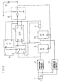
- Fig. 2 is a block diagram illustrating a structure of a data carrier in accordance with a first embodiment of the present invention.
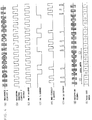
- Fig. 3 is a waveform diagram showing a waveform of each portion at the time of writing data.
- Fig. 4 is a waveform diagram showing a waveform of each portion at the time of reading data.
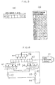
- Fig. 5 is a diagram illustrating one example of data containing identification codes to be written into a shift register and an example of patterns of the identification codes.
- Fig. 6 is a circuit diagram illustrating a read out circuit of data containing the identification codes provided on the side of a write/read control unit.
- Fig. 7 is a block diagram illustrating a structure of a data carrier in accordance with a second embodiment of the present invention.
- Fig. 8 is a circuit diagram illustrating a read out circuit of data containing identification codes used on the side of the write/read control unit.
- Fig. 9 is a block diagram illustrating a structure of a data carrier in accordance with a third embodiment of the present invention.
- Fig. 10 is a waveform diagram showing a waveform of each portion at the time of reading data in this embodiment.
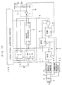
- Fig. 11 is a block diagram illustrating an overall structure of a data carrier in accordance with a sixth embodiment of the present invention.
- Fig. 12 is a block diagram illustrating a structure of a clear signal detecting portion of the data carrier in accordance with the fourth embodiment.
- Fig. 13 is a waveform diagram showing a waveform of each portion at the time of writing data.
- Fig. 14 is a waveform diagram showing a waveform of each portion at the time of reading data.
- Fig. 15 is a waveform diagram showing a waveform of each portion at the time of clearing data of the data carrier.
- Fig. 2 is a block diagram illustrating a structure of a data carrier in accordance with one embodiment of the present invention.
- the data carrier has a resonance circuit 1 including a coil L for reception and a capacitor C and supplies an externally applied PWM modulated signal to a waveform shaping circuit 2.
- Waveform shaping circuit 2 obtains a reception signal corresponding to the intermittence of the supplied signal by envelop detecting the supplied signal and discriminating the same with respect to a predetermined level, and the output thereof is supplied to a multiplexer (MPX) 3 and a monostable multivibrator (MM) 4.
- Monostable multivibrator 4 delays the supplied reception signal by a half period, and the output thereof is supplied to a shift register 5 as a shift pulse.
- Shift register 5 is formed of 8 bits, for example, and the output of multiplexer 3 is supplied to the data input terminal thereof.
- the data output of the shift register 5 is supplied to the set input terminal of a flipflop (FF) 6, the input terminal of an AND circuit 7 and the other input terminal of multiplexer 3.
- a clear signal source 8 is provided including a resistor and a capacitor connected to a power supply in series and an inverter connected to the middle point therebetween. Clear signal source 8 supplies a clear signal, which attains H level after the power supply is turned on and attains L level being delayed for a prescribed period of time, to a clear input terminal of shift register 5 and a reset input terminal of flipflop 6.
- Flipflop 6 switches the input of multiplexer 3 by its Q output, so that the output (Y 0 ) of the above-mentioned waveform shaping circuit 2 is supplied to the input side (IN) of the shift register when the Q output is at L level and the data out input (Y 1 ) of shift register 5 is supplied when it is at H level.
- multiplexer 3 and flipflop 6 constitute signal switching means 9 for switching the input signal to shift register 5.
- the output of monostable multivibrator 4 is also supplied to AND circuit 7.
- AND circuit 7 supplies its logical product output to a monostable multivibrator 10 at the time of reading data.
- Monostable multivibrator 10 is operated for a short period of time in response to data read out from shift register 5 and the output thereof is supplied to a vibration absorbing circuit 11. Vibration absorbing circuit 11 stops reverberations of the received signal by closing a switching element for grounding the both terminals of resonance circuit 1 when a signal of H level is supplied.
- a back-up battery 12 for holding data of shift register 5 is provided for this data carrier.
- data is written into the data carrier by resetting shift register 5 and flipflop 6 using clear signal source 8 and then supplying a signal having different duty ratios in a fixed period to the reception coil of the data carrier.
- Such a structure of the write/read control unit for the data carrier is the same as that shown in the above-mentioned conventional one.
- a signal of H level is supplied to shift register 5 and flipflop 6 from clear signal source 8 for a short period of time, to clear shift register 5 and the flipflop is reset.
- a write/read control unit (not shown) supplies a signal of discontinuous waveform having a fixed period T and a duty ratio corresponding to data to be written. For example, a signal having a duty ratio of 70% is supplied at logic "1" and a signal having a duty ratio of 30% is supplied at logic "0", to reception coil L as shown in Fig. 3(b).
- the signal is received by resonance circuit 1, envelop detected by waveform shaping circuit 2 and discriminated with respect to a predetermined level, so that a signal as shown in Fig. 3(c) is obtained.
- This signal is supplied to monostable multivibrator 4 to be supplied to shift register 5 as a signal 1/2 period delayed from the rising point and having a duty ratio of almost 50% as shown in Fig. 3(d).
- flipflop 6 is reset, the output of waveform shaping circuit 2 is directly written into shift register 5 through multiplexer 3.
- shift register 5 has a structure of 8 bits, when data of 8 bits is written as shown in Fig. 3(e), the output at data output terminal of shift register 5 attains H level.
- flipflop 6 is inverted and then the output of shift register 5 is directly supplied to the input of shift register 5 through multiplexer 3. Accordingly, even if data is transmitted, the data is not written in a duplicated way, data of shift register 5 circulates and the data is held in shift register 5. In this case, it is necessary to set data to be written at first to "1" in order to change shift register 5 from a write mode to a circulation mode. In this way, writing of data is finished after the signal is written into shift register 5 as shown in Fig. 3(e).
- the write/read control unit in reading data from the data carrier, supplies a signal having a fixed duty ratio, for example, 50% in the same period as the period at the time of the above-mentioned data writing as shown in Fig. 4(a). Then, the signal is shaped through resonance circuit 1 and waveform shaping circuit 2 and a signal shown in Fig. 4(b) is supplied from waveform shaping circuit 2. Then, a signal delayed by a half period is obtained from monostable multivibrator 4 as shown in Fig. 4(c) and this signal is applied to shift register 5 as a shift pulse. Accordingly, a signal is read out from shift register 5 corresponding to the shift pulse as shown in Fig. 4(d).
- a signal having a fixed duty ratio for example, 50% in the same period as the period at the time of the above-mentioned data writing as shown in Fig. 4(a).
- a signal is supplied from AND circuit 7 as shown in Fig. 4(e), which attains "H” level when a logic signal "1” is read out and attains "L” level when "0" is read out. Then, this signal is supplied to vibration absorbing circuit 11 by monostable multivibrator 10 as a vibration absorption control signal for a short period of time of a half period or less. Vibration absorbing circuit 11 closes a switching element connected to the both terminals of resonance circuit 1, so that reverberations are inhibited in the period when this signal is being supplied as shown in Fig. 4(a). Accordingly, as shown in Fig.
- a signal is obtained at the both terminals of resonance circuit 1, with reverberations when the logic signal is at H with a fixed duty ratio and without reverberations when the logic signal is 0. Since this signal is also detected on the side of a read/write head (not shown) in the same way, the read/write head can read out the signal written into shift register 5 based on the presence or absence of reverberations as shown in Fig. 4(g) and (h).
- a data length is, for example, 8 bits
- the first 2 bits a and b and the last 2 bits c and d are identification codes ID as shown in Fig. 5(a)
- 4 bits therebetween are bits which the user can use at his option.
- code patterns which the identification codes can take become those as shown in Fig. 5(b).
- the patterns of the identification codes can not be arbitrarily determined and have a limitation as follows.
- the first identification code a needs to be 1 since the shift register is to be switched from the write mode to the circulation mode. Accordingly, the patterns 1 to 4 can not be taken. If the first identification codes "ab" coincide with the last identification codes "cd", data is read out in cycles, so that it becomes impossible to determine which are the head identification codes. Accordingly, a and b can not coincide with c and d at the same time and the patterns 1 and 8 can not be taken. Therefore, a possible identification code pattern is any of 5, 6 and 7 in Fig. 5(b). In the embodiment stated above, there is shown a case where the pattern of 7 is used as identification codes (ID) as shown in Figs. 3 and 4.
- ID identification codes
- Fig. 6 is a diagram illustrating one example of such a code identification circuit.
- the write/read control unit waveform-shapes the output of a data receiving circuit 21 to supply the same to a shift register 22 of 8 bits. Then, the first 2 bits and the last 2 bits are compared, respectively, by digital comparators 23 and 24.
- a register 26 for temporarily holding data is connected to the intermediate 4 bit output terminals of shift register 22. Then, when a coincidence signal is supplied from AND circuit 25, the operation of shift register 22 is stopped, and the intermediate 4 bits are saved in register 26, and serial data is read out from this register 26. In this way, any data written into the shift register of the data carrier can be read out again.
- the present invention may be applied to other structures.
- the first 4 bits and the last 4 bits for example, are used as identification codes, and arbitrary data of 8 bits may be written therebetween.
- the numbers of first and last bits need not be necessarily the same and any number can also be chosen.
- the shift register is used as a memory of the data carrier. Accordingly, once data is written, it is held as it is and then the data can be read out repeatedly by externally supplying a signal of a prescribed duty ratio. Additionally, if reading is stopped halfway, the intermediate write data interposed between the identification codes can be certainly read out. Accordingly, an effect can be attained that a data carrier of a small storage capacity can be made with a highly simplified structure.
- a data carrier according to a second embodiment will now be described with reference to Fig. 7.
- the voltage drop of a battery of the data carrier can be recognized on the side of a read/write head.
- a voltage detection circuit 31 for a battery 12 for detecting the drop of the terminal voltage and the output thereof is supplied to a signal inversion circuit 32.
- Signal inversion circuit 32 given a signal read from a shift register 5, inverts the signal when the drop of the voltage is detected and supplies data through an AND circuit 7.
- the signal read out from shift register 5 is supplied to AND circuits 33 and 34 of signal inversion circuit 32 and the respective outputs are supplied to an OR circuit 36 directly and through an inverter 35.
- OR circuit 36 supplies a logical sum signal of these outputs to AND circuit 7.
- Voltage detection circuit 31 supplies a signal at L level when the voltage level is high and a signal at H level when the voltage drops, to the inversion input terminals of AND circuit 33 and AND circuit 34.
- the output of a monostable multivibrator 4 is also supplied to AND circuit 7.
- AND circuit 7 supplies a logical product output of the logical sum signal of OR circuit 36 and a delay signal to a monostable multivibrator 10.
- Other structures are the same as those in the first embodiment stated above.
- the operation in this embodiment will now be described.
- the data writing process is the same as that in the first embodiment stated above, and at the time of reading data as well, if the output of voltage detection circuit 31 is at L level, the signal read out from shift register in synchronization with a shift pulse applied to shift register 5 is provided to AND circuit 7 through AND circuit 34 and OR circuit 35. Accordingly, the signal is read out in the same way as in the first embodiment.
- Fig. 8 is a block diagram illustrating one example of such a code identifying circuit. In this figure, portions the same as those in Fig. 6 stated above are given the same reference designations and a detailed description thereof will be omitted.
- comparators 41 and 42 are provided in parallel for digital comparators 23 and 24, respectively, for holding identification codes obtained by inverting the logics.
- An OR circuit 44 is provided for taking a logical sum of AND circuits 25 and 43 and the logical sum output is supplied to a shift register 26. Then, if a coincidence signal is supplied from either one of AND circuits 25 and 43, the operation of shift register 26 is stopped through OR circuit 44, the intermediate 4 bits are saved in register 26, and serial data is read out from this register 26. In this way, arbitrary data written into the shift register of the data carrier can be read out again.
- FIG. 9 is a block diagram showing the overall structure of a data carrier in accordance with this embodiment.
- the output of a resonance circuit 1 is shaped by a waveform shaping circuit and supplied to a shift register 5 through a multiplexer 3 and, at the same time, the output of a monostable multivibrator 4 is supplied to the shift register as a shift pulse in the same way as in the first embodiment.
- the output of the monostable multivibrator 4 is supplied to an AND circuit 7 and a counter 90 as well in this embodiment.
- Counter 90 is cleared by a clear signal source 8 and counts the output pulses of monostable multivibrator 4 and inverts the output with the input of the same number of bits as that of shift register 5, i.e., 8 bits in this embodiment.
- the output of counter 90 is supplied to AND circuit 7 and an AND circuit 91.
- AND circuits 7 and 91 supply their logical product signals to a monostable multivibrator 93 through an OR circuit 92.
- Monostable multivibrator 93 is operated for a short time in response to the data read from the shift register 5 and the clock pulse and the output thereof is supplied to an AND circuit 94.
- the Q output of a flipflop 6 is supplied to the other input terminal of AND circuit 94 and its logical product signal is applied to a vibration absorbing circuit 11.
- AND circuits 7, 91 and OR circuit 92 form read out data selecting means 95 for selecting a shaping pulse of a waveform shaping circuit 2 and an output pulse from shift register 5.
- Vibration absorbing circuit 11 is provided for stopping reverberations of the received signal by closing a switching element for grounding the both terminals of resonance circuit 1 when a signal of H level is supplied.
- a battery 12 for backup for holding data of shift register 5 is provided for this data carrier.
- data is written into the data carrier by resetting shift register 5 and flipflop 6 using clear signal source 8 and then applying a signal of different duty ratios in a fixed period to a coil L for reception of the data carrier.
- a structure of a write/read control unit for such a data carrier is the same as the one shown in the conventional example stated above.
- a signal is obtained from counter 90 of 8 bits, which repeats H and L levels every time 8 bits are read out as shown in Fig. 10(h). While counter 90 is at H level, a signal of NRZ "10110011" as shown in Fig. 10(i) and (k) is outputted from AND circuit 7 by the logical product of this clock and the read output of shift register 5 and supplied to monostable multivibrator 93 through OR circuit 92. Accordingly, a signal as shown in Fig. 10(i) is supplied from monostable multivibrator 93.
- Monostable multivibrator 93 generates a vibration absorption control signal and supplies the same to vibration absorbing circuit 11 at the time of falling of the input pulse for a short period of time of 1/2 period or less. Vibration absorbing circuit 11 closes a switching element connected to the both terminals of resonance circuit 1. Then, the amplitude of the resonance is stopped by this pulse as shown in Fig. 10(b). Accordingly, a signal as shown in Fig. 10(m) is received at the reception block diagram of a read/write head (not shown), and data can be received by demodulating this signal.
- AND circuit 7 places an inhibition when counter 90 of 8 bits attains L level, so that the output of shift register 5 is not read out and, in return, the clock signal is read out as it is from AND circuit 11 as shown in Fig. 10(d) and (j). Accordingly, the clock pulse is supplied to monostable multivibrator 93 through OR circuit 92 as shown in Fig. 10(k), and a vibration absorption pulse as shown in Fig. 10(l) is supplied to resonance circuit 1. Therefore, during that time, reception of the read/write head is always 0. Then, when counter 90 attains H level again, the data is sequentially read out following a start bit 1 read out from shift register 5 and a vibration absorption pulse is generated through AND circuit 7.
- Reverberations are inhibited as shown in Fig. 10(b) during a period when this pulse is supplied. Accordingly, a signal is obtained, with reverberations when the logic signal is H with a constant duty ratio, and without reverberations when the logic signal is 0 at the both terminals of resonance circuit 1 as shown in Fig. 10(b). Since this signal is also detected in the same way on the side of a read/write head (not shown), the read/write head can read out a signal written into shift register 5 based on the presence or absence of the reverberations as shown in Fig. 10(h) and (i).
- data can be stored using the first 1 bit of the shift register as a start bit (ST) and the portion other than that as data bits (in this case, 7 bits). Bits for identifying a frame are used so that the start position of data can be correctly recognized at the next time of reading even if reading of data is stopped halfway. Then, it is possible to clearly recognize the data portion by reading out frame identification bits for the bit lines using a counter of the bit lines the same as that of the shift register.
- ST start bit
- the present invention even if reading is stopped halfway, it is possible, in the next reading, to certainly read out the written data from a start bit after the frame identification bits are ended.
- the number of bits obtained by subtracting 1 bit from the bit number of the shift register can be used as a user area, and an effect can be obtained that a data carrier of a small storage capacity can be made with a highly simplified structure.
- FIG. 11 is a block diagram illustrating the overall structure of a data carrier in accordance with this embodiment
- Fig. 12 is a block diagram illustrating a structure of a clear signal detecting portion. Portions the same as those in the first embodiment stated above are given the same reference designations in these figures and detailed descriptions thereof will be omitted here.
- the output of a waveform shaping circuit 2 is supplied to monostable multivibrators 101 and 102 in addition to a multiplexer 3.
- Monostable multivibrator 101 generates a clock signal with a duty ratio of 40% based on the applied received signal as will be stated later and monostable multivibrator 102 generates a clock signal with a duty ratio of 50% based on the received signal as stated below.
- the output of monostable multivibrator 101 is applied to a shift register 5 and a shift register 104 of a clear signal detecting portion 103 as a shift pulse.
- the clear signal detecting portion causes the input applied to shift register 104 to be at L level all the time when the Q output of a flipflop 6 is at L level, and causes the output of waveform shaping circuit 2 to be the input of shift register 104 when Q is at H level.
- Shift register 104 of clear signal detecting portion 103 is a shift register of 1/2 of the number of bits of shift register 5, i.e., 4 bits in this embodiment, and each bit thereof is applied to a comparator 106 of a digital type.
- comparator 106 detects the data string and supplies the same to a shunt circuit 107.
- Shunt circuit 107 clears each portion by grounding the output terminal of a clear signal source 8.
- the output of monostable multivibrator 102 is supplied to an AND circuit 7.
- AND circuit 7 supplies a logical product of input signals to a monostable multivibrator 10 and generates a vibration absorption pulse in the same way as in the above-mentioned first embodiment.
- (a) to (k) indicate waveforms of a to k in Fig. 11.
- a clear signal from clear signal source 8 resets shift register 5 and flipflop 6.
- a waveform in which a signal of a fixed period T is intermittently generated is inputted with a duty ratio corresponding to data to be written from a read/write control unit (not shown).
- a signal of a duty ratio of 70% at logic "1" and of a duty ratio of 30% at logic "0" is supplied as shown in Fig. 13(b) and supplied to a coil L for reception.
- the signal is received by resonance circuit 1 and envelop detected by waveform shaping circuit 2, and a signal as shown in Fig. 13(c) can be obtained by discriminating the same with respect to a predetermined level.
- This signal is supplied to monostable multivibrator 101 and applied to shift register 5 as a signal of a duty ratio of 40% dividing the period T into 4:6 as shown in Fig. 13(d). Since flipflop 6 is reset at first, the output of waveform shaping circuit 2 is written into shift register 5 through multiplexer 3.
- shift register 5 has a structure of 8 bits
- the output of the data output terminal of shift register 5 attains H level.
- flipflop 6 is inverted and then the output of shift register 5 is supplied to the input of shift register 5 through multiplexer 3 as it is. Therefore, even if data is transmitted, the data is not written in a duplicated way and data of shift register 5 circulates, so that the data is held in shift register 5.
- data to be written (start bit) at first should be "1" in order to change shift register 5 from the write mode to the circulation mode in the same way as in the first embodiment.
- the write/read control unit supplies a signal of a fixed duty ratio, for example, 50% in the same period as that at the time of writing data.
- the signal is shaped through resonance circuit 1 and waveform shaping circuit 2 and this waveform is shaped by waveform shaping circuit 2.
- a signal of a duty ratio 40% is outputted from monostable multivibrator 101 as shown in Fig. 14(d) and this signal is supplied to shift register 5 as a shift pulse.
- data "11010001" of NRZ held is read out from shift register 5, corresponding to the shift pulse as shown in Fig. 14(g).
- a signal of a duty ratio of 50% is applied to AND circuit 10 by monostable multivibrator 102, in synchronization with the output of waveform shaping circuit 2 as shown in Fig. 14(h). Accordingly, a logical product signal shown in Fig. 14(i) is supplied from AND circuit 10 and provided to monostable multivibrator 10.
- a vibration absorption control signal is generated and supplied to a vibration absorbing circuit 11 at the time of falling of the input pulse for a short period of time of 1/2 period or less in monostable multivibrator as shown in Fig. 14(j). Vibration absorbing circuit 11 closes a switching element connected to the both terminals of resonance circuit 1. Then, this pulse stops reverberations of resonance as shown in Fig. 14(b). Therefore, a signal of reverberations is received at the receiving portion of a read/write head (not shown) and data can be received by demodulating this signal.
- Two monostable multivibrators 101 and 102 are employed for generating a signal having different duty ratios in this embodiment. If monostable multivibrator 102 of a duty ratio of 50% is employed for the shift pulse of shift register 5, there is a provability that it coincides with the clear command at the time of reading data by chance, and in this case, the data is removed. Therefore, it is necessary to prevent such a situation before it happens. It is possible to prevent the removal of data and absorb the vibration in accordance with the signal from the read/write head by employing monostable multivibrator 101 of a duty ratio of 40% for reading data and monostable multivibrator 102 of a duty ratio of 50% for generating a vibration absorption pulse.
- data within a data carrier can be removed and new data can be written by sending a clear command from the side of the read/write head. Accordingly, an effect can be obtained in which a data carrier for a wider variety of purposes and capable of writing and erasing a small amount of data can be made with a highly simplified structure.
Landscapes
- Engineering & Computer Science (AREA)
- General Physics & Mathematics (AREA)
- Theoretical Computer Science (AREA)
- Physics & Mathematics (AREA)
- Microelectronics & Electronic Packaging (AREA)
- Computer Vision & Pattern Recognition (AREA)
- Computer Networks & Wireless Communication (AREA)
- Computer Hardware Design (AREA)
- Artificial Intelligence (AREA)
- Near-Field Transmission Systems (AREA)
- Materials For Medical Uses (AREA)
- Liquid Crystal (AREA)
- Holo Graphy (AREA)
- Measurement And Recording Of Electrical Phenomena And Electrical Characteristics Of The Living Body (AREA)
- Magnetic Heads (AREA)
- Dc Digital Transmission (AREA)
Abstract
Description
- The present invention relates to data carriers provided for control of tools for machine tools, parts and products in a factory, or an article identification system such as a physical distribution system.
- Conventionally, in order to mechanize control of tools for machine tools or identification and so on of parts and products at an assembly carriage line in a factory, there is a need for a system for identifying and controlling various kinds of articles such as tools, parts, products and so on. There has been proposed an article identification system, as disclosed in Japanese JP-A-1-151832, in which a data carrier having a memory is provided for an article to be identified, necessary information is externally written into the memory of data carrier by data transmission, and the information is read out as required.
- In such a data carrier, as shown in Fig. 1, a
resonance circuit 201 is connected to a coil for reception, a signal obtained at the resonance circuit is waveform shaped in awaveform shaping circuit 202, data is written into amemory 204 through amemory control portion 203 including a gate array, a CPU and so on, or data is read out based on a command given and is supplied by absorbing the vibration ofresonance circuit 201 by avibration absorbing circuit 205. - However, such a conventional data carrier was so structured that it could have a memory of a relatively large storage capacity. Accordingly, the memory control portion formed of the gate array, the CPU and so on became complicated and a memory having a large storage capacity was used, so that it had a disadvantage that the price thereof could not be reduced. Therefore, disadvantageously, it was not suitable for a case where such a memory of a large storage capacity is not required and a small storage capacity, for example, a storage capacity of a memory of several bits to several tens of bits was large enough.
- From FR-A-2 522 850 a data carrier employing ultrasonic wave data transmission is known which has a shift register for circulating and holding data obtained from an input circuit and has signal switching means for switching the input supplied to the shift register from the output of the input circuit to the output of the shift register, in response to an output of the shift register.
- From Patent Abstracts of Japan, vol. 13, no. 480 (P-952), 31.10.89 & JP-A-11 89 791 a data carrier is known with parallel data input into a shift register by means of switches. JP-A-51 150 917 shows a data carrier using electromagnetic coupling and having a shift register for data storage.
- The present invention is made in view of such a problem of a conventional data carrier, and an object thereof is to make it possible to hold a small amount of data with a highly simplified structure suitable for a reduced storage capacity and to write and read data using a conventional write/read control unit as it is.
- The invention is as defined in
claim 1. - Fig. 1 is a block diagram illustrating one example of a conventional data carrier.
- Fig. 2 is a block diagram illustrating a structure of a data carrier in accordance with a first embodiment of the present invention.
- Fig. 3 is a waveform diagram showing a waveform of each portion at the time of writing data.
- Fig. 4 is a waveform diagram showing a waveform of each portion at the time of reading data.
- Fig. 5 is a diagram illustrating one example of data containing identification codes to be written into a shift register and an example of patterns of the identification codes.
- Fig. 6 is a circuit diagram illustrating a read out circuit of data containing the identification codes provided on the side of a write/read control unit.
- Fig. 7 is a block diagram illustrating a structure of a data carrier in accordance with a second embodiment of the present invention.
- Fig. 8 is a circuit diagram illustrating a read out circuit of data containing identification codes used on the side of the write/read control unit.
- Fig. 9 is a block diagram illustrating a structure of a data carrier in accordance with a third embodiment of the present invention.
- Fig. 10 is a waveform diagram showing a waveform of each portion at the time of reading data in this embodiment.
- Fig. 11 is a block diagram illustrating an overall structure of a data carrier in accordance with a sixth embodiment of the present invention.
- Fig. 12 is a block diagram illustrating a structure of a clear signal detecting portion of the data carrier in accordance with the fourth embodiment.
- Fig. 13 is a waveform diagram showing a waveform of each portion at the time of writing data.
- Fig. 14 is a waveform diagram showing a waveform of each portion at the time of reading data.
- Fig. 15 is a waveform diagram showing a waveform of each portion at the time of clearing data of the data carrier.
- Fig. 2 is a block diagram illustrating a structure of a data carrier in accordance with one embodiment of the present invention. In this figure, the data carrier has a
resonance circuit 1 including a coil L for reception and a capacitor C and supplies an externally applied PWM modulated signal to awaveform shaping circuit 2.Waveform shaping circuit 2 obtains a reception signal corresponding to the intermittence of the supplied signal by envelop detecting the supplied signal and discriminating the same with respect to a predetermined level, and the output thereof is supplied to a multiplexer (MPX) 3 and a monostable multivibrator (MM) 4.Monostable multivibrator 4 delays the supplied reception signal by a half period, and the output thereof is supplied to ashift register 5 as a shift pulse.Shift register 5 is formed of 8 bits, for example, and the output ofmultiplexer 3 is supplied to the data input terminal thereof. The data output of theshift register 5 is supplied to the set input terminal of a flipflop (FF) 6, the input terminal of anAND circuit 7 and the other input terminal ofmultiplexer 3. Aclear signal source 8 is provided including a resistor and a capacitor connected to a power supply in series and an inverter connected to the middle point therebetween.Clear signal source 8 supplies a clear signal, which attains H level after the power supply is turned on and attains L level being delayed for a prescribed period of time, to a clear input terminal ofshift register 5 and a reset input terminal offlipflop 6. Flipflop 6 switches the input ofmultiplexer 3 by its Q output, so that the output (Y0) of the above-mentionedwaveform shaping circuit 2 is supplied to the input side (IN) of the shift register when the Q output is at L level and the data out input (Y1) ofshift register 5 is supplied when it is at H level. In this case,multiplexer 3 andflipflop 6 constitute signal switching means 9 for switching the input signal to shiftregister 5. - The output of
monostable multivibrator 4 is also supplied toAND circuit 7. ANDcircuit 7 supplies its logical product output to amonostable multivibrator 10 at the time of reading data.Monostable multivibrator 10 is operated for a short period of time in response to data read out fromshift register 5 and the output thereof is supplied to avibration absorbing circuit 11.Vibration absorbing circuit 11 stops reverberations of the received signal by closing a switching element for grounding the both terminals ofresonance circuit 1 when a signal of H level is supplied. A back-upbattery 12 for holding data ofshift register 5 is provided for this data carrier. - In this case, data is written into the data carrier by resetting
shift register 5 andflipflop 6 usingclear signal source 8 and then supplying a signal having different duty ratios in a fixed period to the reception coil of the data carrier. Such a structure of the write/read control unit for the data carrier is the same as that shown in the above-mentioned conventional one. - The operation in this embodiment will now be described. When the power supply is turned on before writing data, a signal of H level is supplied to shift
register 5 andflipflop 6 fromclear signal source 8 for a short period of time, to clearshift register 5 and the flipflop is reset. Thereafter, a write/read control unit (not shown) supplies a signal of discontinuous waveform having a fixed period T and a duty ratio corresponding to data to be written. For example, a signal having a duty ratio of 70% is supplied at logic "1" and a signal having a duty ratio of 30% is supplied at logic "0", to reception coil L as shown in Fig. 3(b). As a result, the signal is received byresonance circuit 1, envelop detected bywaveform shaping circuit 2 and discriminated with respect to a predetermined level, so that a signal as shown in Fig. 3(c) is obtained. This signal is supplied tomonostable multivibrator 4 to be supplied to shiftregister 5 as asignal 1/2 period delayed from the rising point and having a duty ratio of almost 50% as shown in Fig. 3(d). At first, sinceflipflop 6 is reset, the output ofwaveform shaping circuit 2 is directly written intoshift register 5 throughmultiplexer 3. Asshift register 5 has a structure of 8 bits, when data of 8 bits is written as shown in Fig. 3(e), the output at data output terminal ofshift register 5 attains H level. As a result,flipflop 6 is inverted and then the output ofshift register 5 is directly supplied to the input ofshift register 5 throughmultiplexer 3. Accordingly, even if data is transmitted, the data is not written in a duplicated way, data ofshift register 5 circulates and the data is held inshift register 5. In this case, it is necessary to set data to be written at first to "1" in order to changeshift register 5 from a write mode to a circulation mode. In this way, writing of data is finished after the signal is written intoshift register 5 as shown in Fig. 3(e). - Reading of data will now be described. The write/read control unit, in reading data from the data carrier, supplies a signal having a fixed duty ratio, for example, 50% in the same period as the period at the time of the above-mentioned data writing as shown in Fig. 4(a). Then, the signal is shaped through
resonance circuit 1 andwaveform shaping circuit 2 and a signal shown in Fig. 4(b) is supplied fromwaveform shaping circuit 2. Then, a signal delayed by a half period is obtained frommonostable multivibrator 4 as shown in Fig. 4(c) and this signal is applied to shiftregister 5 as a shift pulse. Accordingly, a signal is read out fromshift register 5 corresponding to the shift pulse as shown in Fig. 4(d). In this case, a signal is supplied from ANDcircuit 7 as shown in Fig. 4(e), which attains "H" level when a logic signal "1" is read out and attains "L" level when "0" is read out. Then, this signal is supplied tovibration absorbing circuit 11 bymonostable multivibrator 10 as a vibration absorption control signal for a short period of time of a half period or less.Vibration absorbing circuit 11 closes a switching element connected to the both terminals ofresonance circuit 1, so that reverberations are inhibited in the period when this signal is being supplied as shown in Fig. 4(a). Accordingly, as shown in Fig. 4(a), a signal is obtained at the both terminals ofresonance circuit 1, with reverberations when the logic signal is at H with a fixed duty ratio and without reverberations when the logic signal is 0. Since this signal is also detected on the side of a read/write head (not shown) in the same way, the read/write head can read out the signal written intoshift register 5 based on the presence or absence of reverberations as shown in Fig. 4(g) and (h). - If 8 or more bits are successively read out, the same data is repeatedly outputted. Even if reading of data is not necessarily carried out on a 8-bit basis and reading of data is stopped halfway, as well, it is necessary to make it possible to read the data. A description will now be made of a structure of identification codes for making it possible. Suppose that a data length is, for example, 8 bits, the first 2 bits a and b and the last 2 bits c and d are identification codes ID as shown in Fig. 5(a), and 4 bits therebetween are bits which the user can use at his option. Then, code patterns which the identification codes can take become those as shown in Fig. 5(b). The patterns of the identification codes, however, can not be arbitrarily determined and have a limitation as follows. That is, the first identification code a needs to be 1 since the shift register is to be switched from the write mode to the circulation mode. Accordingly, the
patterns ① to ④ can not be taken. If the first identification codes "ab" coincide with the last identification codes "cd", data is read out in cycles, so that it becomes impossible to determine which are the head identification codes. Accordingly, a and b can not coincide with c and d at the same time and thepatterns - It is necessary to make it possible to correctly read out data written by the user even if reading is started from halfway along the data of 8 bits obtained in such a way on the side of the write/read control unit. Fig. 6 is a diagram illustrating one example of such a code identification circuit. In this figure, the write/read control unit waveform-shapes the output of a
data receiving circuit 21 to supply the same to ashift register 22 of 8 bits. Then, the first 2 bits and the last 2 bits are compared, respectively, bydigital comparators respective comparators circuit 25. Aregister 26 for temporarily holding data is connected to the intermediate 4 bit output terminals ofshift register 22. Then, when a coincidence signal is supplied from ANDcircuit 25, the operation ofshift register 22 is stopped, and the intermediate 4 bits are saved inregister 26, and serial data is read out from thisregister 26. In this way, any data written into the shift register of the data carrier can be read out again. - While the shift register of the data carrier has a structure of 8 bits in this embodiment, the present invention may be applied to other structures. For example, when a shift register having a structure of 16 bits, the first 4 bits and the last 4 bits, for example, are used as identification codes, and arbitrary data of 8 bits may be written therebetween. In the identification codes, the numbers of first and last bits need not be necessarily the same and any number can also be chosen.
- As described in detail, in accordance with this embodiment, the shift register is used as a memory of the data carrier. Accordingly, once data is written, it is held as it is and then the data can be read out repeatedly by externally supplying a signal of a prescribed duty ratio. Additionally, if reading is stopped halfway, the intermediate write data interposed between the identification codes can be certainly read out. Accordingly, an effect can be attained that a data carrier of a small storage capacity can be made with a highly simplified structure.
- A data carrier according to a second embodiment will now be described with reference to Fig. 7. In this embodiment, the voltage drop of a battery of the data carrier can be recognized on the side of a read/write head. In this figure, portion the same as those in the above-mentioned first embodiment are given the same reference designations and a detailed description thereof will be omitted. In this embodiment, there is provided a
voltage detection circuit 31 for abattery 12 for detecting the drop of the terminal voltage and the output thereof is supplied to asignal inversion circuit 32.Signal inversion circuit 32, given a signal read from ashift register 5, inverts the signal when the drop of the voltage is detected and supplies data through an ANDcircuit 7. - The signal read out from
shift register 5 is supplied to ANDcircuits signal inversion circuit 32 and the respective outputs are supplied to anOR circuit 36 directly and through aninverter 35. ORcircuit 36 supplies a logical sum signal of these outputs to ANDcircuit 7.Voltage detection circuit 31 supplies a signal at L level when the voltage level is high and a signal at H level when the voltage drops, to the inversion input terminals of ANDcircuit 33 and ANDcircuit 34. The output of amonostable multivibrator 4 is also supplied to ANDcircuit 7. ANDcircuit 7 supplies a logical product output of the logical sum signal ofOR circuit 36 and a delay signal to amonostable multivibrator 10. Other structures are the same as those in the first embodiment stated above. - The operation in this embodiment will now be described. The data writing process is the same as that in the first embodiment stated above, and at the time of reading data as well, if the output of
voltage detection circuit 31 is at L level, the signal read out from shift register in synchronization with a shift pulse applied to shiftregister 5 is provided to ANDcircuit 7 through ANDcircuit 34 and ORcircuit 35. Accordingly, the signal is read out in the same way as in the first embodiment. - On the other hand, when the voltage level of
battery 12 drops and the output ofvoltage detection circuit 31 attains H level, the signal read out fromshift register 5 is inverted through ANDcircuit 33,inverter 35 and ORcircuit 36 ofsignal inversion circuit 32 and applied tomonostable multivibrator 10. Accordingly, all data is inverted and supplied to the side of the read/write head. - It is necessary to make it possible to correctly read out data written by the user on the side of the write/read control unit even if reading is started somewhere along the data of 8 bits obtained in this way. Fig. 8 is a block diagram illustrating one example of such a code identifying circuit. In this figure, portions the same as those in Fig. 6 stated above are given the same reference designations and a detailed description thereof will be omitted. In this identifying circuit,
comparators digital comparators comparators circuit 43. An ORcircuit 44 is provided for taking a logical sum of ANDcircuits shift register 26. Then, if a coincidence signal is supplied from either one of ANDcircuits shift register 26 is stopped through ORcircuit 44, the intermediate 4 bits are saved inregister 26, and serial data is read out from thisregister 26. In this way, arbitrary data written into the shift register of the data carrier can be read out again. In this case, as stated above, when the voltage of abattery 12 is normal, data is read out by the coincidence signal from ANDcircuit 25, and when the voltage drops, it is read out by the coincidence signal from ANDcircuit 43, so that it is possible to recognize the written data as well as the state of the battery by identifying data obtained along with this coincidence signal. Additionally, data is not lost due to the drop of the battery voltage, having the effect of being able to enhance the reliability. - A third embodiment in accordance with the present invention will now be described. In this embodiment, data of an amount almost equal to the storage capacity of a shift register within a data carrier can be stored without employing identification codes. Fig. 9 is a block diagram showing the overall structure of a data carrier in accordance with this embodiment. In this figure, portions the same as those in the above-mentioned first embodiment are given the same reference designations and a detailed description thereof will be omitted. In this embodiment, the output of a
resonance circuit 1 is shaped by a waveform shaping circuit and supplied to ashift register 5 through amultiplexer 3 and, at the same time, the output of amonostable multivibrator 4 is supplied to the shift register as a shift pulse in the same way as in the first embodiment. - The output of the
monostable multivibrator 4 is supplied to an ANDcircuit 7 and acounter 90 as well in this embodiment.Counter 90 is cleared by aclear signal source 8 and counts the output pulses ofmonostable multivibrator 4 and inverts the output with the input of the same number of bits as that ofshift register 5, i.e., 8 bits in this embodiment. The output ofcounter 90 is supplied to ANDcircuit 7 and an AND circuit 91. ANDcircuits 7 and 91 supply their logical product signals to amonostable multivibrator 93 through an ORcircuit 92.Monostable multivibrator 93 is operated for a short time in response to the data read from theshift register 5 and the clock pulse and the output thereof is supplied to an AND circuit 94. The Q output of aflipflop 6 is supplied to the other input terminal of AND circuit 94 and its logical product signal is applied to avibration absorbing circuit 11. In this case, ANDcircuits 7, 91 and ORcircuit 92 form read out data selecting means 95 for selecting a shaping pulse of awaveform shaping circuit 2 and an output pulse fromshift register 5.Vibration absorbing circuit 11 is provided for stopping reverberations of the received signal by closing a switching element for grounding the both terminals ofresonance circuit 1 when a signal of H level is supplied. Abattery 12 for backup for holding data ofshift register 5 is provided for this data carrier. - In this case, data is written into the data carrier by resetting
shift register 5 andflipflop 6 usingclear signal source 8 and then applying a signal of different duty ratios in a fixed period to a coil L for reception of the data carrier. A structure of a write/read control unit for such a data carrier is the same as the one shown in the conventional example stated above. - The operation in accordance with this embodiment will now be described. Since writing of data is the same as that in the above-mentioned first embodiment, a description thereof will be omitted here. At the time of reading data, when the write/read control unit reads data from the data carrier, a signal is supplied, having a constant duty ratio, for example, 50% in the same period as that at the time of writing data. As a result, the signal is shaped through
resonance circuit 1 andwaveform shaping circuit 2. Accordingly, a signal shown in Fig. 10(d) is outputted frommonostable multivibrator 4 and this signal is supplied to shiftregister 5, ANDcircuit 7 and counter 90 as a clock pulse. Therefore, a signal is read out fromshift register 5 corresponding to the shift pulse as shown in Fig. 10(g). A signal is obtained from counter 90 of 8 bits, which repeats H and L levels everytime 8 bits are read out as shown in Fig. 10(h). Whilecounter 90 is at H level, a signal of NRZ "10110011" as shown in Fig. 10(i) and (k) is outputted from ANDcircuit 7 by the logical product of this clock and the read output ofshift register 5 and supplied tomonostable multivibrator 93 through ORcircuit 92. Accordingly, a signal as shown in Fig. 10(i) is supplied frommonostable multivibrator 93.Monostable multivibrator 93 generates a vibration absorption control signal and supplies the same tovibration absorbing circuit 11 at the time of falling of the input pulse for a short period of time of 1/2 period or less.Vibration absorbing circuit 11 closes a switching element connected to the both terminals ofresonance circuit 1. Then, the amplitude of the resonance is stopped by this pulse as shown in Fig. 10(b). Accordingly, a signal as shown in Fig. 10(m) is received at the reception block diagram of a read/write head (not shown), and data can be received by demodulating this signal. - Though AND
circuit 7 places an inhibition when counter 90 of 8 bits attains L level, so that the output ofshift register 5 is not read out and, in return, the clock signal is read out as it is from ANDcircuit 11 as shown in Fig. 10(d) and (j). Accordingly, the clock pulse is supplied tomonostable multivibrator 93 through ORcircuit 92 as shown in Fig. 10(k), and a vibration absorption pulse as shown in Fig. 10(l) is supplied toresonance circuit 1. Therefore, during that time, reception of the read/write head is always 0. Then, whencounter 90 attains H level again, the data is sequentially read out following astart bit 1 read out fromshift register 5 and a vibration absorption pulse is generated through ANDcircuit 7. Reverberations are inhibited as shown in Fig. 10(b) during a period when this pulse is supplied. Accordingly, a signal is obtained, with reverberations when the logic signal is H with a constant duty ratio, and without reverberations when the logic signal is 0 at the both terminals ofresonance circuit 1 as shown in Fig. 10(b). Since this signal is also detected in the same way on the side of a read/write head (not shown), the read/write head can read out a signal written intoshift register 5 based on the presence or absence of the reverberations as shown in Fig. 10(h) and (i). In this way, data can be stored using the first 1 bit of the shift register as a start bit (ST) and the portion other than that as data bits (in this case, 7 bits). Bits for identifying a frame are used so that the start position of data can be correctly recognized at the next time of reading even if reading of data is stopped halfway. Then, it is possible to clearly recognize the data portion by reading out frame identification bits for the bit lines using a counter of the bit lines the same as that of the shift register. - As has been described in detail, in accordance with the present invention, even if reading is stopped halfway, it is possible, in the next reading, to certainly read out the written data from a start bit after the frame identification bits are ended. As no identification code is used in this embodiment, the number of bits obtained by subtracting 1 bit from the bit number of the shift register can be used as a user area, and an effect can be obtained that a data carrier of a small storage capacity can be made with a highly simplified structure.
- A sixth embodiment of the present invention will now be described. In this embodiment, data within a shift register is removed by externally sending a clear command to a data carrier, and new data can be arbitrarily written. Fig. 11 is a block diagram illustrating the overall structure of a data carrier in accordance with this embodiment and Fig. 12 is a block diagram illustrating a structure of a clear signal detecting portion. Portions the same as those in the first embodiment stated above are given the same reference designations in these figures and detailed descriptions thereof will be omitted here. In this embodiment, the output of a
waveform shaping circuit 2 is supplied to monostable multivibrators 101 and 102 in addition to amultiplexer 3. Monostable multivibrator 101 generates a clock signal with a duty ratio of 40% based on the applied received signal as will be stated later and monostable multivibrator 102 generates a clock signal with a duty ratio of 50% based on the received signal as stated below. The output of monostable multivibrator 101 is applied to ashift register 5 and ashift register 104 of a clear signal detecting portion 103 as a shift pulse. The clear signal detecting portion, as shown in Fig. 12, causes the input applied to shiftregister 104 to be at L level all the time when the Q output of aflipflop 6 is at L level, and causes the output ofwaveform shaping circuit 2 to be the input ofshift register 104 when Q is at H level.Shift register 104 of clear signal detecting portion 103 is a shift register of 1/2 of the number of bits ofshift register 5, i.e., 4 bits in this embodiment, and each bit thereof is applied to acomparator 106 of a digital type. When a parallel signal ofshift register 104 is a prescribed command, for example, "0011",comparator 106 detects the data string and supplies the same to a shunt circuit 107. Shunt circuit 107 clears each portion by grounding the output terminal of aclear signal source 8. The output of monostable multivibrator 102 is supplied to an ANDcircuit 7. ANDcircuit 7 supplies a logical product of input signals to amonostable multivibrator 10 and generates a vibration absorption pulse in the same way as in the above-mentioned first embodiment. - The operation in accordance with this embodiment will now be described with reference to the waveform diagrams in Figs. 13 to 15. In these figures,(a) to (k) indicate waveforms of a to k in Fig. 11. Firstly, when the power supply is turned on before writing data, a clear signal from
clear signal source 8 resetsshift register 5 andflipflop 6. Then, a waveform in which a signal of a fixed period T is intermittently generated is inputted with a duty ratio corresponding to data to be written from a read/write control unit (not shown). For example, a signal of a duty ratio of 70% at logic "1" and of a duty ratio of 30% at logic "0" is supplied as shown in Fig. 13(b) and supplied to a coil L for reception. In this way, the signal is received byresonance circuit 1 and envelop detected bywaveform shaping circuit 2, and a signal as shown in Fig. 13(c) can be obtained by discriminating the same with respect to a predetermined level. This signal is supplied to monostable multivibrator 101 and applied to shiftregister 5 as a signal of a duty ratio of 40% dividing the period T into 4:6 as shown in Fig. 13(d). Sinceflipflop 6 is reset at first, the output ofwaveform shaping circuit 2 is written intoshift register 5 throughmultiplexer 3. - As
shift register 5 has a structure of 8 bits, when data of 8 bits is written as shown in Fig. 13(e), the output of the data output terminal ofshift register 5 attains H level. As a result, as shown in Fig. 13(f),flipflop 6 is inverted and then the output ofshift register 5 is supplied to the input ofshift register 5 throughmultiplexer 3 as it is. Therefore, even if data is transmitted, the data is not written in a duplicated way and data ofshift register 5 circulates, so that the data is held inshift register 5. In this case, data to be written (start bit) at first should be "1" in order to changeshift register 5 from the write mode to the circulation mode in the same way as in the first embodiment. - Reading of data will now be described with reference to the waveform diagram of Fig. 14. The write/read control unit supplies a signal of a fixed duty ratio, for example, 50% in the same period as that at the time of writing data. In this way, the signal is shaped through
resonance circuit 1 andwaveform shaping circuit 2 and this waveform is shaped bywaveform shaping circuit 2. Accordingly, a signal of a duty ratio 40% is outputted from monostable multivibrator 101 as shown in Fig. 14(d) and this signal is supplied to shiftregister 5 as a shift pulse. As a result, data "11010001" of NRZ held is read out fromshift register 5, corresponding to the shift pulse as shown in Fig. 14(g). At this time, a signal of a duty ratio of 50% is applied to ANDcircuit 10 by monostable multivibrator 102, in synchronization with the output ofwaveform shaping circuit 2 as shown in Fig. 14(h). Accordingly, a logical product signal shown in Fig. 14(i) is supplied from ANDcircuit 10 and provided tomonostable multivibrator 10. A vibration absorption control signal is generated and supplied to avibration absorbing circuit 11 at the time of falling of the input pulse for a short period of time of 1/2 period or less in monostable multivibrator as shown in Fig. 14(j).Vibration absorbing circuit 11 closes a switching element connected to the both terminals ofresonance circuit 1. Then, this pulse stops reverberations of resonance as shown in Fig. 14(b). Therefore, a signal of reverberations is received at the receiving portion of a read/write head (not shown) and data can be received by demodulating this signal. - When a signal of 4 bits with a
duty ratio 70% or 30%, for example, "0011" is sent as a clear command from the read/write head as shown in Fig. 15(b), the signal is also simultaneously transmitted to shiftregister 104. Shunt circuit 107 provides a detection signal of the clear command obtained by detecting this signal bycomparator 106. Shunt circuit 107 grounds the output terminal ofclear signal source 8 for a certain period of time as shown in Fig. 15(k). Accordingly, the clear operation is carried out again and data ofshift register 5 is cleared. Thereafter, another data can be written in the data carrier as stated above by sending new data from the side of the read/write head. - Two monostable multivibrators 101 and 102 are employed for generating a signal having different duty ratios in this embodiment. If monostable multivibrator 102 of a duty ratio of 50% is employed for the shift pulse of
shift register 5, there is a provability that it coincides with the clear command at the time of reading data by chance, and in this case, the data is removed. Therefore, it is necessary to prevent such a situation before it happens. It is possible to prevent the removal of data and absorb the vibration in accordance with the signal from the read/write head by employing monostable multivibrator 101 of a duty ratio of 40% for reading data and monostable multivibrator 102 of a duty ratio of 50% for generating a vibration absorption pulse. - As has been described in detail, in accordance with this embodiment, data within a data carrier can be removed and new data can be written by sending a clear command from the side of the read/write head. Accordingly, an effect can be obtained in which a data carrier for a wider variety of purposes and capable of writing and erasing a small amount of data can be made with a highly simplified structure.
Claims (9)
- A data carrier comprising:a resonance circuit (1) for receiving a PWM signal having different duty ratios corresponding to write data containing identification codes in a transmission mode and having a fixed duty ratio in a reception mode,a waveform shaping circuit (2) for smoothing and wave-forme shaping the received output obtained at said resonance circuit,a shift register (5) for circulating and holding data, to which a signal obtained from said waveform shaping circuit is supplied as a shift pulse,signal switching means (6) for switching the input supplied to said shift register in response to the logic value of the output data of the final stage of said shift register from the output of said shaping circuit (2) to the output of the shift register (5), anda vibration absorbing circuit (11) for controlling reverberations of said resonance circuit based on a signal read from said shift register when a signal of a fixed duty ratio is supplied in the reception mode.
- The data carrier according to claim 1, comprisinga battery (12) for supplying power to each portion of the data carrier,a voltage detection circuit (31) for detecting the voltage drop of said battery, anda signal inversion circuit (32) for inverting the signal read from said shift register when the drop of the voltage is detected by said voltage detection circuit.
- A data carrier according to claim 1 or 2, comprising:a counter (90) for counting the number of shift pulses to said shift register (5),read data selecting means (95) for selecting a shaping pulse obtained from said waveform shaping circuit and the output of said shift register by the output of said counter (90).
- The data carrier according to claim 3, wherein said counter (90) inverts the output when it counts the same number of bits as that of said shift register (5).
- A data carrier according to anyone of the preceding claims, comprising:
a clear signal detecting portion (103) for detecting a clear command obtained by said waveform shaping circuit (2) and resetting said shift register (5) at the time of detection. - The data carrier according to claim 1, 2 or 5, wherein said identification codes are recorded, being broken up into the first and last plurality of bits of the bit length of said shift register.
- The data carrier according to claim 6, wherein the first bit of said identification codes is at a logic level for converting the shift register (5) from a write mode to a circulation mode based on the output when data is written into said shift register (5) and the data is read out.
- The data carrier according to claim 5, wherein said clear signal detecting portion (103) includes a shift register (104) to which the output of said waveform shaping circuit (2) is applied, and a comparator (106) for comparing a parallel output of said shift register (104) and a data string of the clear command.
- The data carrier according to claim 5, comprising:a first monostable multivibrator (101) to which the output of said waveform shaping circuit (2) is supplied, for generating a signal of a duty ratio different from those in the reception mode and the transmission mode and supplying the same to said shift register (5) as a shift pulse, anda second monostable multivibrator (102) to which the output of said waveform shaping circuit (2) is applied, for generating a clock signal of a duty ratio equal to that in said reception mode and supplying the clock signal to said vibration absorbing circuit (11).
Applications Claiming Priority (7)
| Application Number | Priority Date | Filing Date | Title |
|---|---|---|---|
| JP24789/90 | 1990-02-02 | ||
| JP2478990A JPH03229382A (en) | 1990-02-02 | 1990-02-02 | Data carrier |
| JP2770890A JPH03231385A (en) | 1990-02-06 | 1990-02-06 | Data carrier |
| JP27708/90 | 1990-02-06 | ||
| JP3561790A JPH03238952A (en) | 1990-02-15 | 1990-02-15 | Data carrier |
| JP35617/90 | 1990-02-15 | ||
| PCT/JP1991/000110 WO1991011784A1 (en) | 1990-02-02 | 1991-01-30 | Data carrier |
Publications (3)
| Publication Number | Publication Date |
|---|---|
| EP0466934A1 EP0466934A1 (en) | 1992-01-22 |
| EP0466934A4 EP0466934A4 (en) | 1993-04-14 |
| EP0466934B1 true EP0466934B1 (en) | 1996-09-25 |
Family
ID=27284788
Family Applications (1)
| Application Number | Title | Priority Date | Filing Date |
|---|---|---|---|
| EP91903623A Expired - Lifetime EP0466934B1 (en) | 1990-02-02 | 1991-01-30 | Data carrier |
Country Status (6)
| Country | Link |
|---|---|
| US (1) | US5274220A (en) |
| EP (1) | EP0466934B1 (en) |
| AT (1) | ATE143516T1 (en) |
| AU (1) | AU7186291A (en) |
| DE (1) | DE69122325T2 (en) |
| WO (1) | WO1991011784A1 (en) |
Families Citing this family (4)
| Publication number | Priority date | Publication date | Assignee | Title |
|---|---|---|---|---|
| DE4243108A1 (en) | 1992-12-18 | 1994-06-23 | Eurosil Electronic Gmbh | IC card |
| JP3451506B2 (en) * | 1995-03-15 | 2003-09-29 | オムロン株式会社 | Data carrier |
| JPH08272924A (en) * | 1995-03-29 | 1996-10-18 | Mitsubishi Electric Corp | IC card |
| EP1158457A1 (en) * | 2000-05-26 | 2001-11-28 | Sony Corporation | Data synchronizer and data synchronization method |
Family Cites Families (11)
| Publication number | Priority date | Publication date | Assignee | Title |
|---|---|---|---|---|
| JPS51150917A (en) * | 1975-06-19 | 1976-12-24 | Nippon Signal Co Ltd:The | Card data discrimination system |
| US4661691A (en) * | 1976-03-02 | 1987-04-28 | Paperless Accounting, Inc. | Proximity data transfer system |
| JPS52150937A (en) * | 1976-06-09 | 1977-12-15 | Matsushita Electric Ind Co Ltd | Data card and its reading system |
| FR2522850B2 (en) * | 1981-03-05 | 1987-06-26 | Dassault Electronique | EXAMPLE CONTROL SYSTEM FOR THE PASSAGE OF TOLL POINTS |
| JPS61210487A (en) * | 1985-03-14 | 1986-09-18 | Nippon Lsi Kaade Kk | Writing and reading method between memory body and device by non-contact system |
| JPS61283981A (en) * | 1985-06-11 | 1986-12-13 | Nippon Denzai Kogyo Kenkyusho:Kk | Integrated circuit card |
| JPS61241887A (en) * | 1985-04-18 | 1986-10-28 | Omron Tateisi Electronics Co | Memory card |
| JPS63112198A (en) * | 1986-10-31 | 1988-05-17 | 株式会社日立製作所 | IC card |
| US4924210A (en) * | 1987-03-17 | 1990-05-08 | Omron Tateisi Electronics Company | Method of controlling communication in an ID system |
| JPH0732369B2 (en) * | 1987-12-09 | 1995-04-10 | オムロン株式会社 | Data communication device |
| JPH01222392A (en) * | 1988-03-01 | 1989-09-05 | Matsushita Electric Ind Co Ltd | Information storing medium |
-
1991
- 1991-01-30 DE DE69122325T patent/DE69122325T2/en not_active Expired - Fee Related
- 1991-01-30 US US07/768,439 patent/US5274220A/en not_active Expired - Lifetime
- 1991-01-30 AU AU71862/91A patent/AU7186291A/en not_active Abandoned
- 1991-01-30 EP EP91903623A patent/EP0466934B1/en not_active Expired - Lifetime
- 1991-01-30 WO PCT/JP1991/000110 patent/WO1991011784A1/en not_active Ceased
- 1991-01-30 AT AT91903623T patent/ATE143516T1/en not_active IP Right Cessation
Also Published As
| Publication number | Publication date |
|---|---|
| DE69122325D1 (en) | 1996-10-31 |
| EP0466934A4 (en) | 1993-04-14 |
| ATE143516T1 (en) | 1996-10-15 |
| WO1991011784A1 (en) | 1991-08-08 |
| AU7186291A (en) | 1991-08-21 |
| EP0466934A1 (en) | 1992-01-22 |
| US5274220A (en) | 1993-12-28 |
| DE69122325T2 (en) | 1997-05-22 |
Similar Documents
| Publication | Publication Date | Title |
|---|---|---|
| EP0166023B1 (en) | Method and system for data compression and restoration | |
| US4310860A (en) | Method and apparatus for recording data on and reading data from magnetic storages | |
| JPS6184138A (en) | Network system | |
| US5274220A (en) | Data carrier | |
| AU626504B2 (en) | Circuit for decoding binary information | |
| US7126994B2 (en) | Communication station and data carrier with improved acknowledgement measures | |
| EP0438460B1 (en) | Data alignment circuit and method for self-clocking encoded data | |
| US4071889A (en) | Central processing apparatus for generating and receiving time division multiplex signals | |
| AU5280590A (en) | Self clocking binary information encoder | |
| US4352181A (en) | Device for synchronising multiplex lines in a time-division exchange | |
| JP2864766B2 (en) | Data carrier | |
| JP2841729B2 (en) | Data carrier | |
| JPH0560133B2 (en) | ||
| SU1378079A1 (en) | Receiver of coded combinations | |
| RU2108659C1 (en) | Adjustable digital delay line | |
| SU1140237A1 (en) | Synchronizing-signal generator with phasing | |
| JP3593813B2 (en) | Identification system | |
| SU720507A1 (en) | Buffer memory | |
| SU1372330A1 (en) | Device for connecting microprocessor with external devices | |
| SU1718184A1 (en) | Programmable controller inputs scanner | |
| US4152731A (en) | Read circuit for distinguishing false peaks in an alternating current playback signal | |
| SU1569878A1 (en) | Device for digit magnetic recording | |
| SU1423981A1 (en) | Program control device | |
| USRE27812E (en) | High density storage anx retrieval system | |
| RU2168856C1 (en) | Staticproof ring counter |
Legal Events
| Date | Code | Title | Description |
|---|---|---|---|
| PUAI | Public reference made under article 153(3) epc to a published international application that has entered the european phase |
Free format text: ORIGINAL CODE: 0009012 |
|
| 17P | Request for examination filed |
Effective date: 19911002 |
|
| AK | Designated contracting states |
Kind code of ref document: A1 Designated state(s): AT BE CH DE DK ES FR GB GR IT LI NL SE |
|
| A4 | Supplementary search report drawn up and despatched |
Effective date: 19930302 |
|
| AK | Designated contracting states |
Kind code of ref document: A4 Designated state(s): AT BE CH DE DK ES FR GB GR IT LI NL SE |
|
| 17Q | First examination report despatched |
Effective date: 19950111 |
|
| GRAH | Despatch of communication of intention to grant a patent |
Free format text: ORIGINAL CODE: EPIDOS IGRA |
|
| GRAH | Despatch of communication of intention to grant a patent |
Free format text: ORIGINAL CODE: EPIDOS IGRA |
|
| GRAA | (expected) grant |
Free format text: ORIGINAL CODE: 0009210 |
|
| AK | Designated contracting states |
Kind code of ref document: B1 Designated state(s): AT BE CH DE DK ES FR GB GR IT LI NL SE |
|
| PG25 | Lapsed in a contracting state [announced via postgrant information from national office to epo] |
Ref country code: LI Effective date: 19960925 Ref country code: GR Free format text: LAPSE BECAUSE OF FAILURE TO SUBMIT A TRANSLATION OF THE DESCRIPTION OR TO PAY THE FEE WITHIN THE PRESCRIBED TIME-LIMIT Effective date: 19960925 Ref country code: ES Free format text: THE PATENT HAS BEEN ANNULLED BY A DECISION OF A NATIONAL AUTHORITY Effective date: 19960925 Ref country code: DK Effective date: 19960925 Ref country code: CH Effective date: 19960925 Ref country code: BE Effective date: 19960925 Ref country code: AT Effective date: 19960925 |
|
| REF | Corresponds to: |
Ref document number: 143516 Country of ref document: AT Date of ref document: 19961015 Kind code of ref document: T |
|
| REF | Corresponds to: |
Ref document number: 69122325 Country of ref document: DE Date of ref document: 19961031 |
|
| ITF | It: translation for a ep patent filed | ||
| ET | Fr: translation filed | ||
| PG25 | Lapsed in a contracting state [announced via postgrant information from national office to epo] |
Ref country code: SE Effective date: 19961225 |
|
| REG | Reference to a national code |
Ref country code: CH Ref legal event code: PL |
|
| PLBE | No opposition filed within time limit |
Free format text: ORIGINAL CODE: 0009261 |
|
| STAA | Information on the status of an ep patent application or granted ep patent |
Free format text: STATUS: NO OPPOSITION FILED WITHIN TIME LIMIT |
|
| 26N | No opposition filed | ||
| PGFP | Annual fee paid to national office [announced via postgrant information from national office to epo] |
Ref country code: GB Payment date: 20011212 Year of fee payment: 12 |
|
| REG | Reference to a national code |
Ref country code: GB Ref legal event code: IF02 |
|
| PGFP | Annual fee paid to national office [announced via postgrant information from national office to epo] |
Ref country code: NL Payment date: 20020116 Year of fee payment: 12 |
|
| PGFP | Annual fee paid to national office [announced via postgrant information from national office to epo] |
Ref country code: FR Payment date: 20030117 Year of fee payment: 13 |
|
| PG25 | Lapsed in a contracting state [announced via postgrant information from national office to epo] |
Ref country code: GB Free format text: LAPSE BECAUSE OF NON-PAYMENT OF DUE FEES Effective date: 20030130 |
|
| PGFP | Annual fee paid to national office [announced via postgrant information from national office to epo] |
Ref country code: DE Payment date: 20030204 Year of fee payment: 13 |
|
| PG25 | Lapsed in a contracting state [announced via postgrant information from national office to epo] |
Ref country code: NL Free format text: LAPSE BECAUSE OF NON-PAYMENT OF DUE FEES Effective date: 20030801 |
|
| GBPC | Gb: european patent ceased through non-payment of renewal fee | ||
| NLV4 | Nl: lapsed or anulled due to non-payment of the annual fee |
Effective date: 20030801 |
|
| PG25 | Lapsed in a contracting state [announced via postgrant information from national office to epo] |
Ref country code: DE Free format text: LAPSE BECAUSE OF NON-PAYMENT OF DUE FEES Effective date: 20040803 |
|
| PG25 | Lapsed in a contracting state [announced via postgrant information from national office to epo] |
Ref country code: FR Free format text: LAPSE BECAUSE OF NON-PAYMENT OF DUE FEES Effective date: 20040930 |
|
| REG | Reference to a national code |
Ref country code: FR Ref legal event code: ST |
|
| PG25 | Lapsed in a contracting state [announced via postgrant information from national office to epo] |
Ref country code: IT Free format text: LAPSE BECAUSE OF NON-PAYMENT OF DUE FEES;WARNING: LAPSES OF ITALIAN PATENTS WITH EFFECTIVE DATE BEFORE 2007 MAY HAVE OCCURRED AT ANY TIME BEFORE 2007. THE CORRECT EFFECTIVE DATE MAY BE DIFFERENT FROM THE ONE RECORDED. Effective date: 20050130 |