EP0465903A1 - Procédé magnétique de controle du transfert d'énergie dans un convertisseur statique - Google Patents
Procédé magnétique de controle du transfert d'énergie dans un convertisseur statique Download PDFInfo
- Publication number
- EP0465903A1 EP0465903A1 EP91110344A EP91110344A EP0465903A1 EP 0465903 A1 EP0465903 A1 EP 0465903A1 EP 91110344 A EP91110344 A EP 91110344A EP 91110344 A EP91110344 A EP 91110344A EP 0465903 A1 EP0465903 A1 EP 0465903A1
- Authority
- EP
- European Patent Office
- Prior art keywords
- transformer
- current
- demagnetization
- control circuit
- voltage
- Prior art date
- Legal status (The legal status is an assumption and is not a legal conclusion. Google has not performed a legal analysis and makes no representation as to the accuracy of the status listed.)
- Granted
Links
Images


Classifications
-
- H—ELECTRICITY
- H02—GENERATION; CONVERSION OR DISTRIBUTION OF ELECTRIC POWER
- H02M—APPARATUS FOR CONVERSION BETWEEN AC AND AC, BETWEEN AC AND DC, OR BETWEEN DC AND DC, AND FOR USE WITH MAINS OR SIMILAR POWER SUPPLY SYSTEMS; CONVERSION OF DC OR AC INPUT POWER INTO SURGE OUTPUT POWER; CONTROL OR REGULATION THEREOF
- H02M3/00—Conversion of dc power input into dc power output
- H02M3/22—Conversion of dc power input into dc power output with intermediate conversion into ac
- H02M3/24—Conversion of dc power input into dc power output with intermediate conversion into ac by static converters
- H02M3/28—Conversion of dc power input into dc power output with intermediate conversion into ac by static converters using discharge tubes with control electrode or semiconductor devices with control electrode to produce the intermediate ac
- H02M3/325—Conversion of dc power input into dc power output with intermediate conversion into ac by static converters using discharge tubes with control electrode or semiconductor devices with control electrode to produce the intermediate ac using devices of a triode or a transistor type requiring continuous application of a control signal
- H02M3/335—Conversion of dc power input into dc power output with intermediate conversion into ac by static converters using discharge tubes with control electrode or semiconductor devices with control electrode to produce the intermediate ac using devices of a triode or a transistor type requiring continuous application of a control signal using semiconductor devices only
- H02M3/33538—Conversion of dc power input into dc power output with intermediate conversion into ac by static converters using discharge tubes with control electrode or semiconductor devices with control electrode to produce the intermediate ac using devices of a triode or a transistor type requiring continuous application of a control signal using semiconductor devices only of the forward type
-
- G—PHYSICS
- G05—CONTROLLING; REGULATING
- G05F—SYSTEMS FOR REGULATING ELECTRIC OR MAGNETIC VARIABLES
- G05F1/00—Automatic systems in which deviations of an electric quantity from one or more predetermined values are detected at the output of the system and fed back to a device within the system to restore the detected quantity to its predetermined value or values, i.e. retroactive systems
- G05F1/10—Regulating voltage or current
- G05F1/12—Regulating voltage or current wherein the variable actually regulated by the final control device is ac
- G05F1/32—Regulating voltage or current wherein the variable actually regulated by the final control device is ac using magnetic devices having a controllable degree of saturation as final control devices
- G05F1/34—Regulating voltage or current wherein the variable actually regulated by the final control device is ac using magnetic devices having a controllable degree of saturation as final control devices combined with discharge tubes or semiconductor devices
- G05F1/38—Regulating voltage or current wherein the variable actually regulated by the final control device is ac using magnetic devices having a controllable degree of saturation as final control devices combined with discharge tubes or semiconductor devices semiconductor devices only
-
- H—ELECTRICITY
- H02—GENERATION; CONVERSION OR DISTRIBUTION OF ELECTRIC POWER
- H02M—APPARATUS FOR CONVERSION BETWEEN AC AND AC, BETWEEN AC AND DC, OR BETWEEN DC AND DC, AND FOR USE WITH MAINS OR SIMILAR POWER SUPPLY SYSTEMS; CONVERSION OF DC OR AC INPUT POWER INTO SURGE OUTPUT POWER; CONTROL OR REGULATION THEREOF
- H02M3/00—Conversion of dc power input into dc power output
- H02M3/22—Conversion of dc power input into dc power output with intermediate conversion into ac
- H02M3/24—Conversion of dc power input into dc power output with intermediate conversion into ac by static converters
- H02M3/28—Conversion of dc power input into dc power output with intermediate conversion into ac by static converters using discharge tubes with control electrode or semiconductor devices with control electrode to produce the intermediate ac
- H02M3/325—Conversion of dc power input into dc power output with intermediate conversion into ac by static converters using discharge tubes with control electrode or semiconductor devices with control electrode to produce the intermediate ac using devices of a triode or a transistor type requiring continuous application of a control signal
- H02M3/335—Conversion of dc power input into dc power output with intermediate conversion into ac by static converters using discharge tubes with control electrode or semiconductor devices with control electrode to produce the intermediate ac using devices of a triode or a transistor type requiring continuous application of a control signal using semiconductor devices only
- H02M3/33569—Conversion of dc power input into dc power output with intermediate conversion into ac by static converters using discharge tubes with control electrode or semiconductor devices with control electrode to produce the intermediate ac using devices of a triode or a transistor type requiring continuous application of a control signal using semiconductor devices only having several active switching elements
Definitions
- the present invention relates to a magnetic process for controlling the transfer of energy in a static converter.
- the object of the present invention is to carry out a magnetic process for controlling the transfer of energy in a static converter requiring neither an auxiliary magnetic circuit nor a control winding so as to reduce the cost of such static converters which can then use current transformers .
- the magnetic method for controlling the transfer of energy in a static converter according to the invention is distinguished by the characteristics listed in claim 1.
- E is a voltage source which supplies the circuit. It can be obtained either by rectification and filtering of an alternative network, or from any source of continuous energy.
- IQS is a quasi sinusoidal current generator.
- IQS is based on a series resonant monointerruptor structure. This IQS current generator supplies a saturated current transformer T.P.
- R is a rectifier which can be simple or double alternation.
- the control circuit makes it possible to vary the average voltage across the terminals of a winding in transient state. So the magnetic material is brought progressive lies at its saturation. We therefore act on the saturation of the magnetic material by the control circuit varying the voltage in transient state across the primary or secondary winding of the transformer. According to this method, it is therefore no longer necessary to have an auxiliary magnetization winding. It is therefore possible to use a usual intensity transformer.
- the regulator C adjusts for each period, either the demagnetization voltage, or the optimal demagnetization time, or the right combination of these two parameters depending on the desired energy transfer.
- the current transformer is saturated for a period varying as a function of the energy to be transmitted to the secondary to adjust the desired output quantity.
- the current transformer is manufactured in the same way as a conventional transformer, the magnetic circuit is toroidal or made up of parts in the shape of U, E, 1 ... etc.
- the windings can be interleaved or not, concentric or in wafers, mounted on the same leg of the magnetic circuit or on different portions. There is no auxiliary control or magnetization circuit.
- FIG. 4 represents a first embodiment of a static converter whose energy transfer is controlled according to the method of the present invention.
- the regulation principle used in this example consists in varying the demagnetization voltage Vr thanks to the regulator C.
- the components K1, C1, D and L constitute the almost sinusoidal IQS current source of constant amplitude.
- K1 is a switch which is open when i reaches a value 11 set by the designer when dimensioning the static converter. Then the current i enters an oscillatory phase, ends up becoming negative and passes through the diode D as soon as the voltage across the terminals of the capacitor C1 is zero. K1 is closed when i tends to become positive again, a new period begins.
- the technology of K1 can be for example bipolar transistor or MOS FET indifferently.
- the components K2, Dp, Ds, Dr and C constitute the circuit for controlling the magnetic state of the transformer.
- K2 is a controlled switch (any technology may be suitable). Its apparent power is very low compared to that of K1. It closes if current i is positive and opens if i is negative.
- the current Ip in the transformer primary can only be positive.
- the diode Dp ensures the continuity of the current i during its negative half-wave.
- the diode Dr allows the demagnetization of the magnetic material during the negative alternation of the current i and that the switch K2 is therefore open.
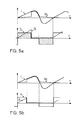
- the control circuit C sets the value of the demagnetization voltage Vr under which the demagnetization takes place. This gives the waveforms of Figures 5a loaded converter and 5b lightly loaded converter.
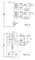
- transformers can be associated in series but each regulated separately, according to the diagram in FIG. 6.
- each of these transformers supplies a control circuit C1, C2, ... controlling the demagnetization of the magnetic circuit of the corresponding transformer.
- each of the transformers is regulated according to the magnetic control method of the energy transfer according to the present invention. It is obvious that each transformer TP1, TP2 ... can have several outputs.
- FIG. 7a shows a first variant of a second embodiment of a static converter for implementing the method.
- the principle of regulation used in this example consists in varying the duration of the demagnetization phase by a regulator C 'which acts on the switch K3.
- the components K1, L, C1 and D constitute the current source IQS described with reference to the first example.
- the switch K3 in parallel with the primary winding of the current transformer T.P., is controlled by the regulator C 'during the negative alternation of the current i.
- K3 When we want to transmit the maximum power to the output, K3 is always open during the period. If the power to be supplied decreases, the regulator C 'closes the switch K3 during the negative alternation of the current i for a period determined as a function of the desired energy transfer.
- the diode D1 When the current Ip at the primary is positive, the diode D1 conducts if the transformer is not saturated.
- FIG. 7b illustrates a second variant of the second exemplary embodiment of a static converter for implementing the method in which the switch K3 and the diode D'p are in parallel with the secondary winding of the current transformer T.P.
- the principle of regulation used in this variant consists in varying the duration of the demagnetization phase by a regulator C "acting on the switch K3.
- the assembly K3, D'p can be mounted either on the main primary or secondary windings of the conventional transformer or on an auxiliary winding of a particular transformer.
- the choice of the winding on which the regulation acts directly is linked to the best compromise between the current flowing in the switch K3 and the voltage at its terminals.
- the inductance L forming part of the current source IQS can be integrated into or constituted by, the leakage inductance of the current transformer TP
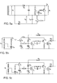
- the regulator C illustrated in FIG. 9a is used in the first embodiment of the static converter illustrated in FIG. 4. It comprises a diode Dr which carries the demagnetization energy of the intensity transformer TP and a transistor T4 which dissipates this energy.
- the transistor T4 When the voltage Vs tends to increase, the transistor T4 conducts and discharges the capacitor CR so that the demagnetization voltage decreases. The magnetic material tends to saturate. It then passes less energy and the voltage VS tends to decrease. The operating point is stable.
- the regulator C 'illustrated in FIG. 9b is used in the variant of the static converter illustrated in FIG. 7a. It includes a reference voltage Vref which is generated by a programmable Zener diode Zp. The current in the diode Do of the optocoupler changes in the same direction as (Vs-Vref), if Vs is the output voltage of the converter.
- the phototransistor To associated with the diode Do behaves like a current source which charges the capacitor C2.
- C2 is then a voltage source whose amplitude increases with the voltage Vs.
- the circuit formed by the components r, C3, D2 and R2 applies a sawtooth voltage on the gate of the transistor T1 which conducts from its control threshold, thus producing the saturation of the transistor T2 and the conduction of the switch K3.
- the switch K3 is actuated in synchronism with the switch K1 and its conduction time is all the longer at each period the greater the output voltage Vs.
- the regulator C "illustrated in FIG. 9c is used in the variant of the static converter illustrated in FIG. 7b, in which the switch K3 and the diode D'p are connected in parallel with the secondary winding of the transformer TP In this case there is no need for galvanic isolation.
- the regulator C " is therefore similar to the regulator C ', the optocoupler (To, Do) being replaced by a simple bipolar transistor pnp To'.
Landscapes
- Engineering & Computer Science (AREA)
- Power Engineering (AREA)
- Automation & Control Theory (AREA)
- Electromagnetism (AREA)
- General Physics & Mathematics (AREA)
- Radar, Positioning & Navigation (AREA)
- Physics & Mathematics (AREA)
- Dc-Dc Converters (AREA)
- Audible-Bandwidth Dynamoelectric Transducers Other Than Pickups (AREA)
- Near-Field Transmission Systems (AREA)
- Inverter Devices (AREA)
- Rectifiers (AREA)
- Control Of Electrical Variables (AREA)
Abstract
Description
- La présente invention a pour objet un procédé magnétique de contrôle du transfert d'énergie dans un convertisseur statique.
- Il est connu, par exemple du brevet US 4.342.075 de commander la puissance délivrée par le secondaire d'un convertisseur statique en agissant sur le flux de fuite ou la saturation d'un transformateur. On dispose un circuit magnétique auxiliaire permettant d'additionner, à l'aide d'un enroulement de commande, un flux dans un circuit magnétique principal comportant les enroulements primaire et secondaire, de manière à en faire varier la perméabilité et donc réguler le transfert d'énergie du primaire au secondaire.
- Cela implique une modification du circuit magnétique du transformateur et l'utilisation d'un enroulement de commande alimenté par un dispositif de commande ou de contrôle du transfert d'énergie.
- La présente invention a pour but la réalisation d un procédé magnétique de contrôle du transfert d'énergie dans un convertisseur statique ne nécessitant ni circuit magnétique auxiliaire ni enroulement de commande de manière à réduire le coût de tels convertisseurs statiques qui peuvent alors utiliser des transformateurs courants.
- Le procédé magnétique de contrôle du transfert d'énergie dans un convertisseur statique selon l'invention se distingue par les caractéristiques énumérées à la revendication 1.
- Le dessin annexé illustre le principe du procédé selon l'invention ainsi que deux modes de mise en oeuvre de celui-ci.
-
- La figure 1 illustre la structure du principe du procédé selon l'invention.
- La figure 2 illustre un modèle équivalent simplifié expliquant le principe de fonctionnement d'un transformateur d'intensité utilisé dans le convertisseur statique.
- Les figures 3a et 3b illustrent le flux magnétique en fonction du courant magnétisant, sans saturation au cours d'une période, respectivement avec saturation pendant une partie de la période de fonctionnement.
- La figure 4 représente une première forme d'exécution d'un convertisseur statique pour la mise en oeuvre du procédé selon l'invention.
- Les figures 5a et 5b illustrent des formes d'ondes de différents paramètres lorsque le convertisseur représenté à la figure 4 est chargé respectivement peu chargé.
- La figure 6 illustre la possibilité d'associer plusieurs transformateurs en série, chacun étant régulé séparemment.
- La figure 7a illustre une première variante d'un second mode de réalisation d'un convertisseur statique pour la mise en oeuvre du procédé selon l'invention.
- La figure 7b illustre une seconde variante du second mode de réalisation d'un convertisseur statique pour la mise en oeuvre du procédé selon l'invention.
- Les figures 8a et 8b illustrent les formes d'ondes de certains paramètres lorsque le convertisseur selon la figure 7 est chargé respectivement peu chargé.
- Les figures 9a, 9b et 9c sont des schémas blocs d'une forme d'exécution des circuits régulateurs C,C' respectivement C" des formes d'exécution illustrées aux figures 4, 7a et 7b respectivement.
- La figure 1 représente la structure de principe du procédé magnétique de contrôle du transfert d'énergie selon l'invention.
- E est une source de tension qui alimente le circuit. Elle peut être obtenue soit par redressement et filtrage d'un réseau alternatif, soit à partir d'une quelconque source d'énergie continue.
- IQS est un générateur de courant quasi sinusoïdal. Dans les exemples de réalisation présentés ci-après, IQS est basé sur une structure monointer- rupteur à résonance série. Ce générateur de courant IQS alimente un transformateur d'intensité saturable T.P.
- R est un redresseur qui peut être simple ou double alternance.
- C est un circuit de contrôle d'une grandeur de sortie, tension, courant, puissance, ... etc, qui permet de maitriser l'état magnétique du transformateur d'intensité saturable T.P.
- Pour expliquer le principe de fonctionnement du transformateur d'intensité selon l'invention, référence est faite au modèle équivalent simplifié de la figure 2, dans lequel Lm est l'inductance magnétisante et T.I. un transformateur d'intensité parfait comportant n1 spires au primaire et n2 spires au secondaire.
- La loi des noeuds donne :
- Ip = Im + (12 . n2/n1)
- Si le circuit magnétique du transformateur est saturé, Lm tend vers zéro et Ip = lm. Il ne passe pas d'énergie vers le secondaire du transformateur.
- Si le circuit magnétique n'est pas saturé, Lm a une valeur finie telle que Im soit très petit par rapport à Ip. Alors, Ip = 12 . n2/n1 et l'énergie est transmise au secondaire.
- Il faut rappeler que la tension moyenne sur une période aux bornes d'un enroulement de transformateur en régime permanent établi est égale à zéro. Ceci est vrai pour tout enroulement de faible résistance interne, aussi bien au primaire, au secondaire, que pour un bobinage auxilaire.
- Selon le présent procédé le circuit de contrôle permet de faire varier la tension moyenne aux bornes d'un bobinage en régime transitoire. Ainsi, le matériau magnétique est amené progressivement à sa saturation. On agit donc sur la saturation du matériau magnétique par le circuit de contrôle faisant varier la tension en régime transitoire aux bornes de l'enroulement primaire ou secondaire du transformateur. Selon ce procédé il n'est donc plus nécessaire de disposer d'un enroulement auxiliaire de magnétisation. On peut donc utiliser un transformateur d'intensité usuel.
- En effet, on peut contrôler la démagnétisation du circuit magnétique par la valeur minimale du courant magnétisant Im selon trois possibilités :
- - En réglant l'amplitude de la tension aux bornes du bobinage primaire ou secondaire pendant la phase de démagnétisation.
- - Sous tension constante, en jouant sur la durée de la démagnétisation.
- - Par combinaison des deux actions ci-dessus.
- On peut suivre aux figures 3a et 3b illustrant le flux magnétique 0 fonction du courant magnétisant Im du matériau, l'évolution de son état magnétique. Au cours d'une période, il n'y a pas saturation dans l'exemple de la figure 3a. Il y a saturation pendant une partie de la période de fonctionnement dans l'exemple de la figure 3b.
- Le régulateur C, ajuste à chaque période, soit la tension de démagnétisation, soit la durée de démagnétisation optimale, soit la bonne combinaison de ces deux paramètres en fonction du transfert d'énergie désiré.
- Ainsi, au cours de chaque période de fonctionnement, le transformateur d'intensité est saturé pendant une durée variant en fonction de l'énergie à transmettre au secondaire pour régler la grandeur de sortie souhaitée.
- Le transformateur d'intensité est fabriqué de la même façon qu'un transformateur usuel, le circuit magnétique est de forme torique ou constitué de pièces en forme de U, de E, de 1 ... etc. Les bobinages peuvent être entrelacés ou non, concentriques ou en galettes, montés sur la même jambe du circuit magnétique ou sur différentes portions. Il ne comporte pas de circuit auxiliaire de contrôle ou de magnétisation.
- La figure 4 représente un premier exemple de réalisation de convertisseur statique dont le transfert d'énergie est contrôlé selon le procédé de la présente invention.
- Le principe de régulation utilisé dans cet exemple consiste à faire varier la tension de démagnétisation Vr grâce au régulateur C.
- Les composants K1, C1, D et L constituent la source de courant IQS quasi sinusoïdal d'amplitude constante.
- K1 est un interrupteur qui est ouvert lorsque i atteint une valeur 11 fixée par le concepteur lors du dimensionnement du convertisseur statique. Puis le courant i entre dans une phase oscillatoire, finit par devenir négatif et passe dans la diode D dès que la tension aux bornes du condensateur C1 est nulle. K1 est fermé lorsque i tend à redevenir positif, une nouvelle période commence. La technologie de K1 peut être par exemple à transistor bipolaire ou MOS FET indifféremment.
- Les composants K2, Dp, Ds, Dr et C constituent le circuit de commande de l'état magnétique du transformateur.
- K2 est un interrupteur commandé (toute technologie peut convenir). Sa puissance apparente est très faible par rapport à celle de K1. Il se ferme si le courant i est positif et s'ouvre si i est négatif.
- Le courant Ip dans le primaire du transformateur ne peut être que positif.
- La diode Dp assure la continuité du courant i pendant son alternance négative.
- Il suffit d'une seule diode Ds de redressement au secondaire. Celle-ci conduit lorsque Ip est positif et que le transformateur n'est pas saturé.
- La diode Dr permet la démagnétisation du matériau magnétique pendant l'alternance négative du courant i et que l'interrupteur K2 est donc ouvert.
- Le circuit de contrôle C règle la valeur de la tension de démagnétisation Vr sous laquelle se fait la démagnétisation. On obtient ainsi les formes d'ondes des figures 5a convertisseur chargé et 5b convertisseur peu chargé.
- Il est à noter que plusieurs transformateurs peuvent être associés en série mais régulés chacun séparemment, selon le schéma de la figure 6.
- On voit dans cette figure que les enroulements primaires de plusieurs transformateurs de courant TP1, TP2... sont branchés en série avec la source de tension E et le générateur d'intensité quasi-sinusoïdal IQS.
- L'enroulement secondaire de chacun de ces transformateurs alimente un circuit de contrôle C1, C2,... commandant la démagnétisaton du circuit magnétique du transformateur correspondant.
- Ainsi chacun des transformateurs est régulé selon le procédé de contrôle magnétique du transfert d'énergie selon la présente invention. Il est évident que chaque transformateur TP1, TP2... peut présenter plusieurs sorties.
- On peut ainsi, avec un seul interrupteur principal, réaliser une alimentation multi-sorties avec des régulations indépendantes de certaines de ces sorties.
- Par exemple, pour un téléviseur, il est possible de réguler dans la structure à résonance monoin- terrupteur décrite, d'une part les alimentations basse tension des circuits électroniques et, d'autre part, les tensions d'accélération et de déviation des plaques (T.H.T.) tout en respectant les distances d'isolement.
- La figure 7a représente une première variante d'un deuxième exemple de réalisation de convertisseur statique pour la mise en oeuvre du procédé.
- Le principe de régulation utilisé dans cet exemple consiste à faire varier la durée de la phase de démagnétisation par un régulateur C' qui agit sur l'interrupteur K3.
- Les composants K1, L, C1 et D constituent la source de courant IQS décrite en référence au premier exemple.
- L'interrupteur K3, en parallèle avec l'enroulement primaire du transformateur d'intensité T.P., est commandé par le régulateur C' pendant l'alternance négative du courant i. Lorsqu'on veut transmettre la puissance maximale à la sortie, K3 est toujours ouvert au cours de la période. Si la puissance à fournir diminue, le régulateur C' ferme l'interrupteur K3 au cours de l'alternance négative du courant i pendant une durée déterminée en fonction du transfert d'énergie désiré.
- Lorsque le courant Ip au primaire est positif, la diode D1 conduit si le transformateur n'est pas saturé.
- Lorsque le courant Ip est négatif, la diode D2 conduit si l'interrupteur K3 est ouvert. Par contre si K3 est fermé, le courant magnétisant Im prend l'amplitude de Ip et la diode D2 est bloquée.
- On obtient les formes d'ondes des figures 8a (convertisseur chargé) et 8b (convertisseur peu chargé).
- La figure 7b illustre une seconde variante du second exemple de réalisation d'un convertisseur statique pour la mise en oeuvre du procédé dans laquelle l'interrupteur K3 et la diode D'p sont en parallèles avec l'enroulement secondaire du transformateur d'intensité T.P.
- Le principe de régulation utilisé dans cette variante consiste à faire varier la durée de la phase de démagnétisation par un régulateur C" agissant sur l'interrupteur K3.
- L'ensemble K3, D'p peut être monté indifféremment sur les bobinages principaux primaire ou secondaire du transformateur conventionnel ou encore sur un bobinage auxiliaire d'un transformateur particulier. Le choix de l'enroulement sur lequel agit directement la régulation est lié au meilleur compromis entre le courant circulant dans l'interrupteur K3 et la tension à ses bornes.
- Il est à noter que dans toutes les formes d'exécution décrites du convertisseur statique pour la mise en oeuvre du procédé, l'inductance L faisant partie de la source de courant IQS peut être intégrée dans Ou constituée par, l'inductance de fuite du transformateur d'intensité T.P.
- Le régulateur C illustré à la figure 9a est utilisé dans la première forme d'exécution du convertisseur statique illustré à la figure 4. Il comporte une diode Dr qui véhicule l'énergie de démagnétisation du transformateur d'intensité T.P. et un transistor T4 qui dissipe cette énergie.
- Lorsque la tension Vs tend à augmenter, le transistor T4 conduit et décharge le condensateur CR de sorte que la tension de démagnétisation diminue. Le matériau magnétique tend à se saturer. Il passe alors moins d'énergie et la tension VS tend à décroître. Le point de fonctionnement est stable.
- Le régulateur C' illustré à la figure 9b est utilisé dans la variante du convertisseur statique illustré à la figure 7a. Il comporte une tension de référence Vref qui est générée par une diode Zener programmable Zp. Le courant dans la diode Do de l'opto- coupleur évolue dans le même sens que (Vs-Vref), si Vs est la tension de sortie du convertisseur.
- Le phototransistor To associé à la diode Do se comporte comme une source de courant qui charge le condensateur C2. C2 est alors une source de tension dont l'amplitude augmente avec la tension Vs.
- Le circuit formé par les composants r, C3, D2 et R2 applique une tension en dent de scie sur la grille du transistor T1 qui conduit à partir de son seuil de commande, produisant ainsi la saturation du transistor T2 et la conduction de l'interrupteur K3.
- L'interrupteur K3 est actionné en synchronisme avec l'interrupteur K1 et sa durée de conduction est d'autant plus longue à chaque période que la tension de sortie Vs est grande.
- Le régulateur C" illustré à la figure 9c est utilisé dans la variante du convertisseur statique illustrée à la figure 7b, dans laquelle l'interrupteur K3 et la diode D'p sont branchés en parallèle avec l'enroulement secondaire du transformateur T.P. Dans ce cas il n'y a pas besoin d'isolement galvanique. Le régulateur C" est donc semblable au régulateur C', l'optocoupleur (To,Do) étant remplacé par un simple transistor bipolaire pnp To'.
Claims (9)
Applications Claiming Priority (4)
| Application Number | Priority Date | Filing Date | Title |
|---|---|---|---|
| CH2343/90A CH683804A5 (fr) | 1990-07-13 | 1990-07-13 | Procédé magnétique de contrôle du transfert d'énergie dans un convertisseur statique et dispositif pour sa mise en oeuvre. |
| CH664/91 | 1991-03-05 | ||
| CH2343/90 | 1991-03-05 | ||
| CH664/91A CH684133A5 (fr) | 1991-03-05 | 1991-03-05 | Procédé magnétique de contrôle du transfert d'énergie dans un convertisseur statique et convertisseur statique pour sa mise en oeuvre. |
Publications (2)
| Publication Number | Publication Date |
|---|---|
| EP0465903A1 true EP0465903A1 (fr) | 1992-01-15 |
| EP0465903B1 EP0465903B1 (fr) | 1996-10-02 |
Family
ID=25685296
Family Applications (1)
| Application Number | Title | Priority Date | Filing Date |
|---|---|---|---|
| EP91110344A Expired - Lifetime EP0465903B1 (fr) | 1990-07-13 | 1991-06-22 | Procédé magnétique de controle du transfert d'énergie dans un convertisseur statique |
Country Status (6)
| Country | Link |
|---|---|
| US (1) | US5184289A (fr) |
| EP (1) | EP0465903B1 (fr) |
| JP (1) | JP2909520B2 (fr) |
| AT (1) | ATE143738T1 (fr) |
| DE (1) | DE69122442T2 (fr) |
| ES (1) | ES2094773T3 (fr) |
Families Citing this family (11)
| Publication number | Priority date | Publication date | Assignee | Title |
|---|---|---|---|---|
| JPH04354266A (ja) * | 1991-05-30 | 1992-12-08 | Sony Corp | 高圧安定化回路 |
| ATE196052T1 (de) * | 1994-04-29 | 2000-09-15 | Andre Bonnet | Statischer wandler mit gesteuertem schalter und steuerungsschaltung |
| KR100413745B1 (ko) * | 1995-08-30 | 2004-03-20 | 정규범 | 컨버터스위치의스위칭손실및노이즈저감회로 |
| US5619402A (en) * | 1996-04-16 | 1997-04-08 | O2 Micro, Inc. | Higher-efficiency cold-cathode fluorescent lamp power supply |
| DE10331866B4 (de) | 2003-07-14 | 2008-11-13 | Minebea Co., Ltd. | Einrichtung zur Steuerung einer Spulenanordnung mit elektrisch variierbarer Induktivität, sowie Schaltnetzteil |
| US20070159856A1 (en) * | 2006-01-11 | 2007-07-12 | Ta-Yung Yang | Flyback power converter with split primary winding transformer |
| US8179699B2 (en) * | 2008-12-31 | 2012-05-15 | Stmicroelectronics S.R.L. | Method for controlling a switching regulator and related switching regulator |
| KR101529146B1 (ko) * | 2014-05-13 | 2015-06-16 | 엘에스산전 주식회사 | 계기용 변압기의 편차 보상 방법 |
| KR101578292B1 (ko) * | 2014-05-13 | 2015-12-16 | 엘에스산전 주식회사 | 계기용 변압기의 편차 보상 방법 |
| KR101622461B1 (ko) * | 2014-05-13 | 2016-05-18 | 엘에스산전 주식회사 | 계기용 변압기의 편차 보상 방법 |
| CN106873461B (zh) * | 2017-03-02 | 2019-02-05 | 国家电网公司 | 一种电流互感器剩磁消磁装置的控制方法 |
Citations (4)
| Publication number | Priority date | Publication date | Assignee | Title |
|---|---|---|---|---|
| US4342075A (en) * | 1977-05-20 | 1982-07-27 | Tdk Electronics | Switched mode DC to DC converter using variable leakage transformer |
| EP0191482A2 (fr) * | 1985-02-12 | 1986-08-20 | Hitachi Metals, Ltd. | Convertisseur courant continu/courant continu |
| EP0255844A1 (fr) * | 1986-08-08 | 1988-02-17 | International Business Machines Corporation | Sources d'alimentation comportant un amplificateur magnétique de régulation de la tension |
| US4864478A (en) * | 1987-12-23 | 1989-09-05 | Bloom Gordon E | Integrated-magnetics power converter |
Family Cites Families (8)
| Publication number | Priority date | Publication date | Assignee | Title |
|---|---|---|---|---|
| NL7309056A (fr) * | 1973-06-29 | 1974-12-31 | ||
| US4652809A (en) * | 1986-01-06 | 1987-03-24 | Microtel Limited | Switched regulator circuit having an extended duty cycle range |
| US4736285A (en) * | 1986-06-19 | 1988-04-05 | Veeco Instruments, Inc. | Demagnetization circuit for forward converter |
| DE3724590A1 (de) * | 1987-07-24 | 1989-02-02 | Gert Guenther Niggemeyer | Gleichspannungswandler |
| US4809148A (en) * | 1987-10-21 | 1989-02-28 | British Columbia Telephone Company | Full-fluxed, single-ended DC converter |
| FR2626419B1 (fr) * | 1988-01-21 | 1990-06-29 | Sgs Thomson Microelectronics | Dispositif de surveillance de demagnetisation pour alimentation a decoupage a regulation primaire et secondaire |
| US4951186A (en) * | 1988-03-04 | 1990-08-21 | Siemens Aktiengesellschaft | Single-ended forward frequency converter with a transformer and a demagnetization means |
| US4969081A (en) * | 1989-01-09 | 1990-11-06 | Sundstrand Corporation | Inverter switch current sensor with shoot-through current limiting |
-
1991
- 1991-06-22 DE DE69122442T patent/DE69122442T2/de not_active Expired - Fee Related
- 1991-06-22 ES ES91110344T patent/ES2094773T3/es not_active Expired - Lifetime
- 1991-06-22 EP EP91110344A patent/EP0465903B1/fr not_active Expired - Lifetime
- 1991-06-22 AT AT91110344T patent/ATE143738T1/de not_active IP Right Cessation
- 1991-07-11 JP JP3171328A patent/JP2909520B2/ja not_active Expired - Lifetime
- 1991-07-15 US US07/731,826 patent/US5184289A/en not_active Expired - Fee Related
Patent Citations (4)
| Publication number | Priority date | Publication date | Assignee | Title |
|---|---|---|---|---|
| US4342075A (en) * | 1977-05-20 | 1982-07-27 | Tdk Electronics | Switched mode DC to DC converter using variable leakage transformer |
| EP0191482A2 (fr) * | 1985-02-12 | 1986-08-20 | Hitachi Metals, Ltd. | Convertisseur courant continu/courant continu |
| EP0255844A1 (fr) * | 1986-08-08 | 1988-02-17 | International Business Machines Corporation | Sources d'alimentation comportant un amplificateur magnétique de régulation de la tension |
| US4864478A (en) * | 1987-12-23 | 1989-09-05 | Bloom Gordon E | Integrated-magnetics power converter |
Also Published As
| Publication number | Publication date |
|---|---|
| ES2094773T3 (es) | 1997-02-01 |
| EP0465903B1 (fr) | 1996-10-02 |
| DE69122442T2 (de) | 1997-04-30 |
| ATE143738T1 (de) | 1996-10-15 |
| JPH04229074A (ja) | 1992-08-18 |
| US5184289A (en) | 1993-02-02 |
| DE69122442D1 (de) | 1996-11-07 |
| JP2909520B2 (ja) | 1999-06-23 |
Similar Documents
| Publication | Publication Date | Title |
|---|---|---|
| EP0680245B1 (fr) | Ensemble comprenant un convertisseur statique à interrupteur commandé et un circuit de commande | |
| FR2543377A1 (fr) | Convertisseur continu-continu regule | |
| FR2590070A1 (fr) | Ensemble magnetique integre destine a etre utilise dans le circuit de sortie d'une alimentation electrique commutee | |
| EP0465903B1 (fr) | Procédé magnétique de controle du transfert d'énergie dans un convertisseur statique | |
| FR2815790A1 (fr) | Convertisseur de tension a circuit de commande autooscillant | |
| EP1040559B1 (fr) | Procede de commande d'un convertisseur de tension continu-continu a stockage inductif | |
| FR2764134A1 (fr) | Unite d'alimentation en courant pour le transfert d'energie par commutation alternative des enroulements d'un transformateur, a grande vitesse | |
| EP0340049A1 (fr) | Dispositif d'alimentation de tube luminescent | |
| FR2740627A1 (fr) | Alimentation a decoupage a correction de facteur de puissance | |
| FR2470500A1 (fr) | Circuit de deviation et d'alimentation en courant avec attaque reduite lors de la mise en marche | |
| FR2816128A1 (fr) | Alimentation a decoupage basse tension isolee | |
| EP0329571B1 (fr) | Dispositif de surveillance de démagnétisation pour alimentation à découpage à régulation primaire et secondaire | |
| FR2488092A1 (fr) | Circuit d'attaque horizontale ferroresonnant | |
| FR2471103A1 (fr) | Circuit d'alimentation en courant de deviation et en energie | |
| CH684133A5 (fr) | Procédé magnétique de contrôle du transfert d'énergie dans un convertisseur statique et convertisseur statique pour sa mise en oeuvre. | |
| EP0022380B1 (fr) | Dispositif d'alimentation par découpage combiné avec un circuit de balayage-ligne d'un récepteur de télévision, régulé par déphasage variable | |
| FR2519207A1 (fr) | Circuit onduleur comportant une commande de symetrie | |
| CH683804A5 (fr) | Procédé magnétique de contrôle du transfert d'énergie dans un convertisseur statique et dispositif pour sa mise en oeuvre. | |
| EP0443342A1 (fr) | Procédé de contrôle du transfert d'énergie dans un convertisseur statique; convertisseur statique d'énergie pour sa mise en oeuvre et alimentation électrique utilisant un tel convertisseur | |
| EP0143048B1 (fr) | Convertisseur continu-continu à inductance de charge commutée | |
| EP0007866B1 (fr) | Circuit d'alimentation stabilisée d'un récepteur vidéofréquence, et récepteur comportant un tel circuit | |
| FR2502418A1 (fr) | Bloc d'alimentation electrique a decoupage pour appareils electroniques | |
| FR2851379A1 (fr) | Convertisseur en transfert direct d'energie | |
| FR2520958A1 (fr) | Circuit auxiliaire pour televiseur | |
| FR2458967A1 (fr) | Dispositif d'alimentation a decoupage regule contre les variations de tension d'entree et de puissance de sortie, notamment pour recepteur de television |
Legal Events
| Date | Code | Title | Description |
|---|---|---|---|
| PUAI | Public reference made under article 153(3) epc to a published international application that has entered the european phase |
Free format text: ORIGINAL CODE: 0009012 |
|
| AK | Designated contracting states |
Kind code of ref document: A1 Designated state(s): AT BE CH DE DK ES FR GB GR IT LI LU NL SE |
|
| 17P | Request for examination filed |
Effective date: 19920321 |
|
| 17Q | First examination report despatched |
Effective date: 19940125 |
|
| GRAG | Despatch of communication of intention to grant |
Free format text: ORIGINAL CODE: EPIDOS AGRA |
|
| GRAH | Despatch of communication of intention to grant a patent |
Free format text: ORIGINAL CODE: EPIDOS IGRA |
|
| GRAH | Despatch of communication of intention to grant a patent |
Free format text: ORIGINAL CODE: EPIDOS IGRA |
|
| GRAA | (expected) grant |
Free format text: ORIGINAL CODE: 0009210 |
|
| AK | Designated contracting states |
Kind code of ref document: B1 Designated state(s): AT BE CH DE DK ES FR GB GR IT LI LU NL SE |
|
| PG25 | Lapsed in a contracting state [announced via postgrant information from national office to epo] |
Ref country code: GR Free format text: LAPSE BECAUSE OF FAILURE TO SUBMIT A TRANSLATION OF THE DESCRIPTION OR TO PAY THE FEE WITHIN THE PRESCRIBED TIME-LIMIT Effective date: 19961002 Ref country code: DK Effective date: 19961002 Ref country code: AT Effective date: 19961002 |
|
| REF | Corresponds to: |
Ref document number: 143738 Country of ref document: AT Date of ref document: 19961015 Kind code of ref document: T |
|
| REF | Corresponds to: |
Ref document number: 69122442 Country of ref document: DE Date of ref document: 19961107 |
|
| ITF | It: translation for a ep patent filed |
Owner name: SPADINI MARUSCO |
|
| PG25 | Lapsed in a contracting state [announced via postgrant information from national office to epo] |
Ref country code: SE Effective date: 19970102 |
|
| REG | Reference to a national code |
Ref country code: CH Ref legal event code: NV Representative=s name: WILLIAM BLANC & CIE CONSEILS EN PROPRIETE INDUSTRI |
|
| GBT | Gb: translation of ep patent filed (gb section 77(6)(a)/1977) |
Effective date: 19961230 |
|
| REG | Reference to a national code |
Ref country code: ES Ref legal event code: FG2A Ref document number: 2094773 Country of ref document: ES Kind code of ref document: T3 |
|
| PG25 | Lapsed in a contracting state [announced via postgrant information from national office to epo] |
Ref country code: LU Free format text: LAPSE BECAUSE OF NON-PAYMENT OF DUE FEES Effective date: 19970630 |
|
| PLBE | No opposition filed within time limit |
Free format text: ORIGINAL CODE: 0009261 |
|
| STAA | Information on the status of an ep patent application or granted ep patent |
Free format text: STATUS: NO OPPOSITION FILED WITHIN TIME LIMIT |
|
| 26N | No opposition filed | ||
| PGFP | Annual fee paid to national office [announced via postgrant information from national office to epo] |
Ref country code: GB Payment date: 19990422 Year of fee payment: 9 |
|
| PGFP | Annual fee paid to national office [announced via postgrant information from national office to epo] |
Ref country code: CH Payment date: 19990525 Year of fee payment: 9 |
|
| PGFP | Annual fee paid to national office [announced via postgrant information from national office to epo] |
Ref country code: NL Payment date: 19990630 Year of fee payment: 9 |
|
| PGFP | Annual fee paid to national office [announced via postgrant information from national office to epo] |
Ref country code: BE Payment date: 19990705 Year of fee payment: 9 |
|
| PGFP | Annual fee paid to national office [announced via postgrant information from national office to epo] |
Ref country code: DE Payment date: 20000509 Year of fee payment: 10 |
|
| PG25 | Lapsed in a contracting state [announced via postgrant information from national office to epo] |
Ref country code: GB Free format text: LAPSE BECAUSE OF NON-PAYMENT OF DUE FEES Effective date: 20000622 |
|
| PGFP | Annual fee paid to national office [announced via postgrant information from national office to epo] |
Ref country code: FR Payment date: 20000623 Year of fee payment: 10 |
|
| PG25 | Lapsed in a contracting state [announced via postgrant information from national office to epo] |
Ref country code: LI Free format text: LAPSE BECAUSE OF NON-PAYMENT OF DUE FEES Effective date: 20000630 Ref country code: CH Free format text: LAPSE BECAUSE OF NON-PAYMENT OF DUE FEES Effective date: 20000630 Ref country code: BE Free format text: LAPSE BECAUSE OF NON-PAYMENT OF DUE FEES Effective date: 20000630 |
|
| PGFP | Annual fee paid to national office [announced via postgrant information from national office to epo] |
Ref country code: ES Payment date: 20000727 Year of fee payment: 10 |
|
| BERE | Be: lapsed |
Owner name: DANNER JEAN-PIERRE Effective date: 20000630 Owner name: BONNET ANDRE Effective date: 20000630 |
|
| PG25 | Lapsed in a contracting state [announced via postgrant information from national office to epo] |
Ref country code: NL Free format text: LAPSE BECAUSE OF NON-PAYMENT OF DUE FEES Effective date: 20010101 |
|
| GBPC | Gb: european patent ceased through non-payment of renewal fee |
Effective date: 20000622 |
|
| REG | Reference to a national code |
Ref country code: CH Ref legal event code: PL |
|
| NLV4 | Nl: lapsed or anulled due to non-payment of the annual fee |
Effective date: 20010101 |
|
| PG25 | Lapsed in a contracting state [announced via postgrant information from national office to epo] |
Ref country code: ES Free format text: LAPSE BECAUSE OF NON-PAYMENT OF DUE FEES Effective date: 20010623 |
|
| PG25 | Lapsed in a contracting state [announced via postgrant information from national office to epo] |
Ref country code: FR Free format text: LAPSE BECAUSE OF NON-PAYMENT OF DUE FEES Effective date: 20020228 |
|
| PG25 | Lapsed in a contracting state [announced via postgrant information from national office to epo] |
Ref country code: DE Free format text: LAPSE BECAUSE OF NON-PAYMENT OF DUE FEES Effective date: 20020403 |
|
| REG | Reference to a national code |
Ref country code: ES Ref legal event code: FD2A Effective date: 20030203 |
|
| PG25 | Lapsed in a contracting state [announced via postgrant information from national office to epo] |
Ref country code: IT Free format text: LAPSE BECAUSE OF NON-PAYMENT OF DUE FEES;WARNING: LAPSES OF ITALIAN PATENTS WITH EFFECTIVE DATE BEFORE 2007 MAY HAVE OCCURRED AT ANY TIME BEFORE 2007. THE CORRECT EFFECTIVE DATE MAY BE DIFFERENT FROM THE ONE RECORDED. Effective date: 20050622 |