EP0465171B1 - A colour liquid crystal display device - Google Patents
A colour liquid crystal display device Download PDFInfo
- Publication number
- EP0465171B1 EP0465171B1 EP91305907A EP91305907A EP0465171B1 EP 0465171 B1 EP0465171 B1 EP 0465171B1 EP 91305907 A EP91305907 A EP 91305907A EP 91305907 A EP91305907 A EP 91305907A EP 0465171 B1 EP0465171 B1 EP 0465171B1
- Authority
- EP
- European Patent Office
- Prior art keywords
- liquid crystal
- crystal display
- light
- micro
- display device
- Prior art date
- Legal status (The legal status is an assumption and is not a legal conclusion. Google has not performed a legal analysis and makes no representation as to the accuracy of the status listed.)
- Expired - Lifetime
Links
Images


Classifications
-
- G—PHYSICS
- G03—PHOTOGRAPHY; CINEMATOGRAPHY; ANALOGOUS TECHNIQUES USING WAVES OTHER THAN OPTICAL WAVES; ELECTROGRAPHY; HOLOGRAPHY
- G03B—APPARATUS OR ARRANGEMENTS FOR TAKING PHOTOGRAPHS OR FOR PROJECTING OR VIEWING THEM; APPARATUS OR ARRANGEMENTS EMPLOYING ANALOGOUS TECHNIQUES USING WAVES OTHER THAN OPTICAL WAVES; ACCESSORIES THEREFOR
- G03B33/00—Colour photography, other than mere exposure or projection of a colour film
- G03B33/10—Simultaneous recording or projection
- G03B33/12—Simultaneous recording or projection using beam-splitting or beam-combining systems, e.g. dichroic mirrors
-
- H—ELECTRICITY
- H04—ELECTRIC COMMUNICATION TECHNIQUE
- H04N—PICTORIAL COMMUNICATION, e.g. TELEVISION
- H04N9/00—Details of colour television systems
- H04N9/12—Picture reproducers
- H04N9/31—Projection devices for colour picture display, e.g. using electronic spatial light modulators [ESLM]
-
- G—PHYSICS
- G02—OPTICS
- G02F—OPTICAL DEVICES OR ARRANGEMENTS FOR THE CONTROL OF LIGHT BY MODIFICATION OF THE OPTICAL PROPERTIES OF THE MEDIA OF THE ELEMENTS INVOLVED THEREIN; NON-LINEAR OPTICS; FREQUENCY-CHANGING OF LIGHT; OPTICAL LOGIC ELEMENTS; OPTICAL ANALOGUE/DIGITAL CONVERTERS
- G02F1/00—Devices or arrangements for the control of the intensity, colour, phase, polarisation or direction of light arriving from an independent light source, e.g. switching, gating or modulating; Non-linear optics
- G02F1/01—Devices or arrangements for the control of the intensity, colour, phase, polarisation or direction of light arriving from an independent light source, e.g. switching, gating or modulating; Non-linear optics for the control of the intensity, phase, polarisation or colour
- G02F1/13—Devices or arrangements for the control of the intensity, colour, phase, polarisation or direction of light arriving from an independent light source, e.g. switching, gating or modulating; Non-linear optics for the control of the intensity, phase, polarisation or colour based on liquid crystals, e.g. single liquid crystal display cells
- G02F1/133—Constructional arrangements; Operation of liquid crystal cells; Circuit arrangements
- G02F1/1333—Constructional arrangements; Manufacturing methods
- G02F1/1335—Structural association of cells with optical devices, e.g. polarisers or reflectors
- G02F1/1336—Illuminating devices
- G02F1/133621—Illuminating devices providing coloured light
-
- H—ELECTRICITY
- H04—ELECTRIC COMMUNICATION TECHNIQUE
- H04N—PICTORIAL COMMUNICATION, e.g. TELEVISION
- H04N9/00—Details of colour television systems
- H04N9/12—Picture reproducers
- H04N9/31—Projection devices for colour picture display, e.g. using electronic spatial light modulators [ESLM]
- H04N9/3102—Projection devices for colour picture display, e.g. using electronic spatial light modulators [ESLM] using two-dimensional electronic spatial light modulators
- H04N9/3105—Projection devices for colour picture display, e.g. using electronic spatial light modulators [ESLM] using two-dimensional electronic spatial light modulators for displaying all colours simultaneously, e.g. by using two or more electronic spatial light modulators
- H04N9/3108—Projection devices for colour picture display, e.g. using electronic spatial light modulators [ESLM] using two-dimensional electronic spatial light modulators for displaying all colours simultaneously, e.g. by using two or more electronic spatial light modulators by using a single electronic spatial light modulator
-
- G—PHYSICS
- G02—OPTICS
- G02F—OPTICAL DEVICES OR ARRANGEMENTS FOR THE CONTROL OF LIGHT BY MODIFICATION OF THE OPTICAL PROPERTIES OF THE MEDIA OF THE ELEMENTS INVOLVED THEREIN; NON-LINEAR OPTICS; FREQUENCY-CHANGING OF LIGHT; OPTICAL LOGIC ELEMENTS; OPTICAL ANALOGUE/DIGITAL CONVERTERS
- G02F1/00—Devices or arrangements for the control of the intensity, colour, phase, polarisation or direction of light arriving from an independent light source, e.g. switching, gating or modulating; Non-linear optics
- G02F1/01—Devices or arrangements for the control of the intensity, colour, phase, polarisation or direction of light arriving from an independent light source, e.g. switching, gating or modulating; Non-linear optics for the control of the intensity, phase, polarisation or colour
- G02F1/13—Devices or arrangements for the control of the intensity, colour, phase, polarisation or direction of light arriving from an independent light source, e.g. switching, gating or modulating; Non-linear optics for the control of the intensity, phase, polarisation or colour based on liquid crystals, e.g. single liquid crystal display cells
- G02F1/133—Constructional arrangements; Operation of liquid crystal cells; Circuit arrangements
- G02F1/1333—Constructional arrangements; Manufacturing methods
- G02F1/1335—Structural association of cells with optical devices, e.g. polarisers or reflectors
- G02F1/1336—Illuminating devices
- G02F1/133621—Illuminating devices providing coloured light
- G02F1/133623—Inclined coloured light beams
Description
- The present invention relates to a color liquid crystal display device having a single liquid crystal display element in which, after a plurality of beams in different wavelength ranges are projected to a single liquid display element respectively from different directions, these beams are combined to display a color image, and particularly to one incorporated in a small-sized color television (TV) system of projection type and an information display system.
- There will be described generally known color liquid crystal display (hereinafter referred to as liquid crystal display) devices of projection type.
- As an alternative to a conventional so-called projection type TV in which an image displayed in a cathode ray tube is projected onto a screen, there has been developed a projection type TV having a liquid crystal display element. Such a TV has already been commercially available. Since the liquid crystal display element is not self-luminous, it is required to provide a light source separately. However, the liquid crystal display element is, in principle, characterized in being capable of displaying as bright an image as possible in accordance with the brightness of the light source. Also, when compared to a projection type color TV having a screen of same size and using the cathode ray tube, the color TV using the liquid crystal display element can be manufactured remarkably small-sized and light-weighted. Accordingly, there are great expectations for development of the liquid crystal display element in future.
- There are known a simple matrix liquid crystal display element and an active matrix liquid crystal display element depending on driving method thereof. The present invention can be applied to both types of liquid crystal display element. Further, as a projection type color image display method using the liquid crystal display element, there are known a three-element display method in which three liquid crystal display elements corresponding to three primary colors are used and a single-element display method in which a single liquid crystal display element is used. According to the three-element display method, optical systems for transmitting respective color lights of three primary colors and display elements for forming an image by controlling respective color lights are provided in pair independently of one another. Images of respective colors are optically superimposed onto one another to display a full color image. Unexamined Japanese Patent Publication JP-A-603291 discloses a display device which has three individual light sources and color filters serving as sources emitting the respective color beams of red, green and blue. However, it is also possible that the light emitted from the single white light source is separated into color beams of three primary colors, i.e., red, green and blue, by dichroic mirrors and the respective color beams are projected onto the liquid crystal display elements corresponding to the respective colors. Such a display device is disclosed by the present applicant in Unexamined Japanese Patent Publication JP-A-60169827. As a white light source, a halogen lamp, xenon lamp, metal halide lamp, or the like can be used. The emission spectrum of the white light source may be continuous spectrum or white light spectrum. With this construction, since the light emitted from the common white light source can be effectively utilized, images are three times as bright as those obtained in the conventional single-element display construction to be described below provided that other conditions are equal. However, more parts are required than the single-element display construction. Accordingly, in terms of cost and size, the above display device is generally disadvantageous compared to the single-element display device. Further, it will be noted that the dichroic mirror is made by forming a dielectric multi-layer thin film with a known thin film formation technique,so as to reflect or transmit only the light having selected wavelength ranges, on a transparent substrate such as glass. Alternatively, the dichroic mirror may be combined in a prism such as a dichroic prism used in an image pick-up device for a color TV, the surface of the prism having similar dielectric multi-layer thin film for selecting the wavelength formed thereon. Hereinafter, the both types of mirrors are merely referred to as dichroic mirrors.
- On the other hand, in the former construction in which only one liquid crystal display element is used, similar to a direct vision liquid crystal TV, the light is projected on a liquid crystal display element having a color filter pattern of three primary colors in the form of mosaic by the use of an optical system similar to a slide projector. Such a construction is, for example, disclosed in Unexamined Japanese Patent Publications JP-A-59131278 and JP-A-59230383. In the case where this single-element display method is adopted, the optical system can be simple in its construction and only one liquid crystal display element is used. Accordingly, the single-element display method is suitable to be adopted in a small-sized projection type system.
- However, according to the single-element display method, about two-thirds of the light projected on the liquid crystal display element is absorbed or reflected by the color filter. For example, a red color filter is arranged on a picture element for displaying red. However, green and blue light are cut by the red color filter. Accordingly, only one-third of the light incident upon the liquid crystal display element can be made use of. Therefore, when compared to the case where three liquid crystal display elements are used with the same light source, the brightness of the screen is reduced to about one-third.
- The conventional projection type color liquid crystal display device is summarily described above. In the singleelement display device, the white light is projected upon the liquid crystal display element and the color display is effected by arranging a micro dichroic mirror, micro-prism array, or diffraction grating for its corresponding group, each group consisting of picture elements of three primary colors. Such a construction is disclosed in Unexamined Japanese Patent Publications JP-A-61210328, JP-A-62293222, JP-A-62293223, and JP-A-63118125. However, it is, in reality, very difficult to form a micro dichroic mirror of about 100µm. Also, when the method is adopted for spectrally resolving the projected light through the use of a micro-prism array or diffraction grating, it is at present difficult to set anaperture efficiency of the picture element sufficiently high. Accordingly, it has been due to shortcomings of the above method that only a portion of the resolved spectral compositions can be made use of.
- It is therefore an object of the invention to improve the brightness of an image on the screen of a color liquid crystal display device.
- The invention, as defined by claim 1, provides a color liquid crystal display device comprising a single liquid crystal display panel, a light-source providing parallel white light, light-projecting means receiving said parallel white light for projecting light beams of respective different wavelengths onto said panel at respective different angles, the panel comprising respective sets of image-modulation elements which are controllable for light-modulation in accordance with the respective color components of an image to be projected by the device, and optical means disposed on the light-receiving side of said liquid crystal display panel for converging the light of said light beams onto the respective corresponding sets of image-modulation elements, characterized in that said light-projecting means comprises a plurality of dichroic mirrors arranged at mutually different angles with respect to the direction of the received parallel white light for generating said light beams as beams having respective predetermined projection angles by reflection of light within respective discrete wavelength ranges.
- The preamble of claim 1 reflects the state of the art according to the aforementioned Unexamined Japanese Patent Publication No. JP-A-63-118125.
- According to the invention, it is possible to realize a small-sized color image display device whose screen is very bright, taking advantage of the single-element structure.
-
- Fig. 1 is a diagram of a color liquid crystal display device for showing an embodiment of the invention;
- Fig. 2(A) is a sectional diagram showing a liquid crystal display element and a micro-lens array used in the embodiment;
- Fig. 2(B) is a plan view of an array pattern of signal electrodes;
- Fig. 2(C) is a perspective view of the micro-lens array;
- Fig. 3(A), 3(B) are plan views of a picture element electrode array and a micro-lens array showing respectively other embodiments of the invention.
- FIG. 1 is a diagram of a light source of a single-element projection type color image display device for showing an embodiment of the invention. Indicated at 1 is a white light source. In this embodiment, a metal halide lamp of 150 W is used as a light source with an arc of the lamp arranged perpendicular to the surface of Fig. 1. An arc length AL and an arc radius Aφ of the lamp are respectively 5 mm and 2.2 mm. It will be noted that a halogen lamp or a xenon lamp can be used as a white light source as well. Behind the white light source 1 is disposed a spherical mirror 2. In front of the white light source 1 is arranged a condenser lens 3 having an aperture of 80 mmφ and a focal length fc of 60 mm. The spherical mirror 2 is arranged with the center thereof corresponding with the center of a light emitting portion of the white light source 1. Further, the white light source 1 is arranged with the center of the light emitting portion thereof corresponding with a focus of the condenser lens 3. With this arrangement, the light projected from the white light source 1 upon the condenser lens 3 becomes beams of white light substantially parallel to one another after transmission through the condenser lens 3. At this time, the degree of parallelization of beams is about 2.2° in the lengthwise direction of the arc of the white light source 1, i.e., in the direction perpendicular to the surface of Fig. 1, and about 1° in the radial direction of the arc, i.e., in the direction parallel to the surface of Fig. 1. Forwardly of the condenser lens 3 there are arranged three kinds of
dichroic mirrors dichroic mirrors dichroic mirrors - The dichroic mirrors 4R, 4G, and 4B are so arranged in this embodiment that an angle of incidence to the
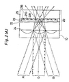
dichroic mirror 4R is around 30° on the optical axis and thedichroic mirrors 4G and 4B are rotated to the left about the direction normal to the surface of Fig. 1 by angles of several degrees from their respective positions parallel to thedichroic mirror 4R. The dichroic mirror 4B is rotated more to the left than thedichroic mirror 4G. The difference in angles of incidence between the two dichroic mirrors is calculated based on an array pitch P of the picture elements of a liquidcrystal display element 20 and a focal length fµ ofmicro-lenses 10. With this arrangement of the optical system, for example, the light in the wavelength range of red light is reflected by thedichroic mirror 4R and incident upon themicro-lens array 10 attached to the liquidcrystal display element 20 disposed on an optical path of the light reflected by thedichroic mirror 4R. The light in the wavelength range of green light is reflected by thedichroic mirror 4G after transmission through thedichroic mirror 4R, and similarly incident upon themicro-lens array 10 at a different angle after transmission again through thedichroic mirror 4R. The light in the wavelength range of blue is reflected by the dichroic mirror 4B after transmission through both thedichroic mirrors micro-lens array 10 at another different angle after transmission again through both thedichroic mirrors micro-lens array 10 from three different directions. It will be noted that an angle of incidence of the white light to thedichroic mirrors - Fig. 2(A) is a sectional diagram of the liquid
crystal display element 20 and themicro-lens array 10 used in the embodiment. As shown in Fig. 2(A), the liquidcrystal display element 20 comprises twoglass substrates liquid crystal layer 23 filled between the twosubstrates signal electrodes scanning electrode 22. Thesignal electrodes scanning electrode 22 constitute a matrix electrode structure so as to drive theliquid crystal 23 according to the simple matrix driving method, and are respectively arranged on the inner surfaces of thesubstrates signal electrodes scanning electrode 22 are all formed by transparent conductive film. To thesignal electrodes dichroic mirror 4R is transmitted via thesignal electrode 21R through themicro-lens array 10. Similarly, the green light reflected by thedichroic mirror 4G is transmitted via thesignal electrode 21G through themicro-lens array 10. Further similarly, the blue light reflected by the dichroic mirror 4B is transmitted via thesignal electrode 21B through themicro-lens array 10. - Fig. 2(B) is a plan view of an array pattern of the
signal electrodes micro-lens array 10 disposed on the surface of liquidcrystal display element 20 facing the light source from the different directions. The beams of respective colors are converged at different positions on themicro-lens array 10. At this time, if the angles of incidence of respective color beams to themicro-lens array 10 are properly selected so as to satisfy a condition to be described below, convergence spots of respective color beams can be made incident upon different apertures of the respective picture elements. This condition is that in the case where a pin hole is placed in the center of the micro-lens, the light passed through the pin hole passes through the center of the aperture of the corresponding picture element. This condition can be expressed as follows.
- In this embodiment, in order to separate the white beams projected from the single white light source 1 into a plurality of color beams, e.g., into beams of three primary colors and make the plurality of color beams incident upon the
micro-lens array 10 from the different directions, thedichroic mirrors dichroic mirrors crystal display element 20. - Next, there will be described a significant element in the embodiment, namely micro-lens
array 10. According to the aforementioned active matrix driving method, in order to supply voltage independently for driving each picture element, an element such as a thin film transistor or MIM (metalinsulator-metal) is provided for each picture element. However, wiring between the picture elements is necessary so as to supply the driving signals to the picture elements. Also, in the case where the light is incident upon regions other than the picture element regions, a black level of the image in the display screen stands out, with the result that contrast of the image is reduced. To prevent this, there is normally provided shadow masks in the non-picture element regions so as to absorb or reflect the light which is not to be used in displaying the image. Accordingly, in the case where a display panel is illuminated at the same illuminance, the smaller is the aperture efficiency of the display panel, the darker the screen is likely to be. In order to overcome such a problem, Unexamined Japanese Patent Publications Nos. JP-A-165621 to 165624 disclose a construction in which a micro-lens array is provided closer to a light source than a display panel and the illuminating light is converged in the respective picture element regions so as to improve the efficiency in the use of the projected light. However, these publications do not specify the kind of the light source, nor the degree of parallelization of the illuminating light. Further, they do not specify the projection of the image. However, upon looking at their constructions, it can be inferred that a visual angle will be expanded. Also, Unexamined Japanese Patent Publication No. JP-A-60-262131 discloses a construction in which a pair of lens elements are provided on both sides of a display panel for each picture element, and the illuminating light incident upon the display panel is converged in a picture element region by the first lens, and then transmitted through the display region. Then, the light diverging at an angle determined by the number of apertures is again converged into a plurality of beams substantially parallel to one another by the second lens. - On the other hand, in a projection type image display device, in the case where a micro-lens array is provided only on a surface of a liquid crystal display element facing a light source, beams substantially parallel to one another which are incident upon the micro-lens array are converged, are transmitted through a picture element region of the liquid crystal display element, and are modulated in accordance with an image signal. Then, the converged beams are diverged within a solid angle determined by the number of aperture (NA) of the micro-lens. However, if the aperture of the projection lens is selected so as to receive the beams, the light transmitted through the liquid crystal display panel is not subject to restriction. More specifically, the light incident upon the liquid crystal display panel and transmitted through the picture element region is effectively used. Accordingly, compared to a projection type image display device not having a micro-lens, a brighter image can be obtained.
- As a formation method of the micro-lens array used for these purposes, the following methods can be considered.
- (1) Method for obtaining a lens of refractive index distribution type by selectively diffusing ions. According to this method, a host glass plate is soaked in fused salt and different alkali ions or the like are exchanged between the glass plate and the fused salt through a mask provided on the glass plate, so that the glass plate having a refractive index distribution corresponding to the mask pattern can be obtained. (Electronics Letters Vol. 17 No. 18 P452 (1981).)
In the case where the micro-lens is fabricated by this method, the lens has no irregularities on an outer surface thereof. Accordingly, such micro-lens can be bound to the liquid crystal display panel with no air there between by the use of Canada balsam and light-hardening resin. Therefore, reflection loss on the surface of the substrate can be reduced to almost negligible. - (2) Method for obtaining a micro-lens by machining the plastic or the glass or molding them by a metal pattern. Besides a direct processing, the metal pattern can be fabricated by using a pattern obtained by the methods described in the following methods (3) to (7) as an original pattern and transferring it through the use of an electroforming technique or the like.
- (3) Method for fabricating a convex lens by using a phenomenon in which, when any of certain kinds of photosensitive resin is exposed in the form of a pattern, unreacted monomers move from a non-exposed portion to an exposed portion, so that the exposed portions are banked. (Applied Physics Society Optics Meeting Microoptics Study Group Journal Vol. 5 NO. 2 p118 (1987), ibid Vol. 6 No. 2 p87 (1988).)
- (4) Method for obtaining a convex lens by patterning thermoplastic resin into a flat form of the lens by the use of a known photographic technique or the like, then heating the same up to a temperature of not lower than a softening point so as to create fluidity to facilitate occurrence of die wear of the edge of the pattern . In this case, if the thermoplastic resin is photosensitive, it can be patterned just by being exposed itself. (Unexamined Japanese Patent Publications No.JP-A-60-38989, No.JP-A-60-165623, and No.JP-A-61-67003.)
- (5) Method for obtaining a convex lens by applying a proximity exposure (an exposure method by which a photomask is not contacted) to photosensitive resin and making the resin have amounts of photoreaction product distributed in accordance with the reduction in intensity of illumination near the edge of the pattern. (Unexamined Japanese Patent Publication No.JP-A-61-153602.)
- (6) Method for obtaining a lens by projecting the light having an intensity distribution to photosensitive resin and forming a pattern of refractive index in accordance with the intensity of the light. (Unexamined Japanese Patent Publication No. JP-A-60-72927.)
(Material whose refractive index is variable in accordance with the projected light is disclosed in Unexamined Japanese Patent Publication No.JP-A-60-166946.) - (7) Method for obtaining a convex lens by projecting the patterned light to photosensitive glass whose photosensitivity is given by applying silver-salt to the glass, having thus produced silver crystalline nucleus grown by heat treatment, and utilizing the volumetric shrinkage accompanied by induced crystallization of the glass. (Applied Optics Vol. 24 No. 16 p2520 (1985).)
- Further, it is disclosed that a micro-lens array and a mosaic color filter are combined to be applied to a liquid crystal display element in Unexamined Japanese Patent Publications No.JP-A-61-208080, No.JP-A-62-94826, No.JP-A-62-203126, No.JP-A-62-267791, and No.JP-A-62-267723. However, these publications do not specify that such a construction can be applied to the projection type display device. Further, in the former four publications, a picture element, a color filter, and a micro-lens correspond to one another as one group. In the last publication, the arrangement is characterized in that a micro convex lens of transparent resin having such a radius to cover three color pixels arranged in line is provided on a color filter.
- In Fig. 2(A), a deflecting plate, an orientation film and the like which are elements of the liquid
crystal display element 20 are omitted for the sake of simplicity. In this embodiment, a simple matrix type liquid crystal display element is used which is operated in a super-twisted nematic (STN) mode in which the number of scanning electrodes is 220, a pitch between the scanning electrodes is 200µm, the number of signal electrodes is 600, and a pitch between the signal electrodes is 100µm. As opposed to a conventional single-element liquid crystal display device, according to the invention, it is not required that the liquid crystal display element be provided with a color filter. However, color allocations of driving signals are longitudinal stripe type and the respective color signals are applied to thesignal electrodes corresponding micro-lens array 10, a lenticular lens substrate is used in which a longitudinal lenticular lens having width of 300µm corresponding to threesignal electrodes glass substrate 24 of the liquidcrystal display element 20. However, when the focal length of the micro-lens is measured in the air, it is calculated based on the following expression to be 0.72 mm.
- Fig. 2(C) is a perspective view showing the
micro-lens array 10. When parallel beams are projected onto themicro-lens array 10 from a predetermined direction, the respective beams are converged in positions, where the optical axes of the respective micro-lenses intersect with liquid crystal layer, at intervals of 300µm correspondingly to the pitch of the lenticular lenses in the form of a line. The width W of the convergence line is:
- Next, when the parallel beams are projected onto the
micro-lens array 10 from the direction inclined by an angle θ (θ = tan-1(100/720)) = 8° from the original direction, the convergence lines shift laterally by 100µm respectively from the original ones and thereby are to be contained in the adjacent signal electrode. Accordingly, the parallel beams of three primary colors are projected onto themicro-lens array 10 from three different directions, the two adjoining directions differing by 8°, the convergence lines of three primary colors are sequentially formed on the adjacent three signal electrodes at the intervals of 100 µm. - When the respective signal electrodes are driven by video signals corresponding to the colors of convergence line formed thereon, the intensities of the light of the respective colors are modulated in accordance with the video signals. The modulated light is further projected onto a
screen 7 through aprojection lens 6 to display a color image thereon (see Fig.1). In order to make an aperture of theprojection lens 6 smaller, it may be appropriate that a field lens 5 be disposed right behind the liquidcrystal display element 20 so as to converge the diverging light after transmission through the liquidcrystal display element 20. - In the conventional single liquid crystal display element provided with a mosaic color filter or a stripe color filter, any of color filters of three primary colors is formed on an upper or lower surface of a picture element electrode. Accordingly, about two-thirds of the light incident upon the liquid crystal display element is cut off. However, in this embodiment, since all the incident light is to be utilized, the brightness of the display screen is improved three-fold compared to the conventional one.
- Instead of the simple matrix type liquid crystal display element used in the first embodiment, there will be described an embodiment in which an active matrix type liquid crystal display element is used. The liquid crystal display element in a twisted nematic (TN) mode is drivingly dynamic-displayed through an amorphous silicon semiconductor thin film for switching rectangular picture elements arranged in the form of a matrix. A delta array is adopted. Picture element pitches are 100µm in both the longitudinal and the lateral directions. Size of an aperture of the picture element is 50 x 70 µm. The number of picture elements is 450 by 600. (450 picture elements are arranged in vertical rows and 600 picture elements are arranged in horizontal columns.) Aperture efficiency of the picture elements is 35 %. Although a light source and dichroic mirrors are disposed in a manner similar to the first embodiment, a metal halide lamp serving as a light source is arranged so that an arc thereof becomes parallel to the surface of Fig 1. In the case where the picture element array is a delta array, the use of lenticular lenses is inappropriate. Forms of each of individual micro-lenses is not necessarily similar to that of the corresponding group of picture elements. Accordingly, a micro-lens array is formed by the ion exchange method in which hexagonal micro-lenses are precisely arrayed. The hexagonal micro-lenses are made by mutually fusing circumferential portions of spherical lenses. Fig. 3(a) shows an example of the relative positional relationship between the picture element array and micro-lens array. In Fig. 3(a), the picture elements are arrayed as if square bricks are arrayed. The hexagonal micro-lenses are arrayed in the form of a honeycomb so as to constitute the micro-lens array. The green light is projected onto both the liquid crystal display element and the micro-lens array from the perpendicular direction (i.e., from the direction perpendicular to the surface of Fig. 3(a), and convergence spots are formed within the green picture elements disposed on the optical axes of the respective micro-lenses. The red and the blue light are projected from the direction tilted by 8° to the left and to the right respectively, and convergence spots of the respective colors are formed within the red and the blue picture elements. In this way, the beams of respective colors are converged in the red, green, and blue picture elements. Size of the convergence spot can be obtained by the calculation similar to that described with reference to the first embodiment, i.e., 60µm × 26.4µm. Therefore, the convergence spot can be contained in the aperture of the picture element.
- Further, in the example shown in Fig. 3(a), three convergence spots of three primary colors converged by one micro-lens are arranged laterally. It may be appropriate that three picture elements are treated as a group as shown in Fig. 3(b) and the corresponding color beams are converged to the respective picture elements. In the latter case, it is required that the direction normal to the surface of the dichroic mirrors shown in Fig. 1 be inclined from the direction of the surface of Fig. 1. However, angles made by the optical axes of the micro-lenses and the illuminating light of respective colors become smaller. Accordingly, aberration of the micro-lens can be reduced.
- Moreover, the order of color separation by the dichroic mirror is not limited to the one described in this embodiment. Further, in this embodiment, the example is illustrated in which a white light is separated into beams of three primary colors. However, the invention can be applied to a construction in which a white light is separated into beams of four or more colors for graphic display.
- The technique for forming the precise array of the micro-lenses is disclosed in Unexamined Japanese Patent Publication No.JP-A-1-275410. According to this technique, boundary lines of the micro-lenses serve as vertical bisector of line segments joining the centers of the adjacent micro-lenses.
- The aforementioned embodiments are described with respect to the projection type liquid crystal display device. If a display screen is formed on the surface of the liquid crystal display device upon which the light is incident through a scattering transmission plate so that the respective transmitted beams are combinedly scattered to form a color image on the display screen, the invention can be incorporated in a direct vision type display device other than the projection type one. Further, the color beams projected from the different directions are distributively projected upon the signal electrodes in units of a beam by the use of the micro-lenses, the color display device receiving color signals corresponding to the respective color beams. Further, the signal electrode may be additionally provided with a function of guiding the light so as to transmit only the beams projected from a predetermined direction, and reflect or absorb the beams projected from other directions. Thereby, only the color beams projected at corresponding angles are to be transmitted through the signal electrode.
- When a single-element projection type color liquid crystal display device as shown in the above embodiment is compared with a conventional single-element projection type color liquid crystal display device having, instead of a micro-lens array, a mosaic color filter, the brightness of the display screen of the former display device is 7.5 times as much as that of the latter one. The improvement in the brightness of the display screen is obtained for the following two reasons. One reason is that in the conventional display device, about two-thirds of the light is cut off by the mosaic color filter. However, in the display device of the embodiment, almost all the light is effectively utilized, thereby increasing the brightness of the display screen about 3 times. The other reason is that in the conventional display device, aperture efficiency of the picture element is 35 %, so that 65 % of the light incident upon the liquid crystal display element is wasted by being cut by the shadow mask. However, in the display device of the embodiment, the incident light is converged in the aperture of the picture element, so that most of the incident light can be effectively utilized.
Consequently, the brightness of the display screen is increased about 2.5 times. Therefore, the brightness of the display screen in the display device of the embodiment is 7.5 (3 × 2.5) times as much as that of the conventional display device. - According to the invention, in the case where degree of parallelization of the illuminating light is bad, and the light is incident upon the liquid crystal display element from the direction different from the predetermined direction, i.e., stray light, there may be possibility of inducing a reduction in contrast on the display screen and also in color purity. Accordingly, it may be appropriate that the white light from the light source is temporarily converged on spots by the condenser lens and the unnecessary light is cut by a slit or a pin hole.
- This invention may be embodied in other forms without departing from the scope thereof as defined by the claims.
Claims (10)
- A color liquid crystal display device comprising a single liquid crystal display panel (20), a light-source (1, 2, 3) providing parallel white light, light-projecting means (4R, 4G, 4B) receiving said parallel white light for projecting light beams (R, G, B) of respective different wavelengths onto said panel at respective different angles, the panel comprising respective sets of image-modulation elements (21R, 21G, 21B) which are controllable for light-modulation in accordance with the respective color components of an image to be projected by the device, and optical means (10) disposed on the light-receiving side of said liquid crystal display panel (20) for converging the light of said light beams (R, G, B) onto the respective corresponding sets of image-modulation elements (21R, 21G, 21B), characterized in that said light-projecting means comprises a plurality of dichroic mirrors (4R, 4G, 4B) arranged at mutually different angles with respect to the direction of the received parallel white light for generating said light beams (R, G, B) as beams having respective predetermined projection angles by reflection of light within respective discrete wavelength ranges.
- A color liquid crystal display device as defined in claim 1, wherein said light-projecting means comprises three said dichroic mirrors (4R, 4G 4B) arranged for splitting said white light into beams of three primary colors.
- A color liquid crystal display device as defined in claim 2, wherein said three light beams (R, G, B) have a first wavelength range of at least 600nm, a second wavelength range of between 500nm and 570nm, and a third wavelength range of at most 500nm, respectively.
- A color liquid crystal display device as defined in any of claims 1 to 3, wherein the liquid crystal display panel (20) comprises a plurality of signal electrodes (21R, 21G, 21B) to each of which a display signal for one color is independently applied so as to drive the pixels of said display panel, each pixel corresponding to one of said image-modulation elements, and said optical means (10) comprises a micro-lens array for converging said respective light beams onto corresponding pixels.
- A color liquid crystal display device as defined in claim 4, wherein the projection angles of the respective light beams incident upon the micro-lens array (10) satisfy the following condition:

- A color liquid crystal display device as defined in claim 4, wherein the micro-lens array (10) is composed of machined glass or plastic having a uniform refractive index.
- A color liquid crystal display device as defined in claim 4, wherein the micro-lens array (10) is composed of a plurality of lenses, each lens having a refractive index distribution produced by a selective ion exchange method.
- A color liquid crystal display device as defined in claim 4, wherein the micro-lens array (10) is composed of a plurality of lenticular lenses and the plurality of signal electrodes (21R, 21G, 21B) are in the form of stripes.
- A color liquid crystal display device as defined in claim 4, wherein the micro-lens array is composed of a plurality of lenses in the form of a honeycomb and said pixels of the display panel form a mosaic or delta arrangement.
- A color liquid crystal display device as defined in any of claims 1 to 4 and 9, wherein said liquid crystal display panel is of active-matrix type.
Applications Claiming Priority (2)
| Application Number | Priority Date | Filing Date | Title |
|---|---|---|---|
| JP171923/90 | 1990-06-28 | ||
| JP2171923A JP2622185B2 (en) | 1990-06-28 | 1990-06-28 | Color liquid crystal display |
Publications (3)
| Publication Number | Publication Date |
|---|---|
| EP0465171A2 EP0465171A2 (en) | 1992-01-08 |
| EP0465171A3 EP0465171A3 (en) | 1992-11-04 |
| EP0465171B1 true EP0465171B1 (en) | 1996-10-16 |
Family
ID=15932357
Family Applications (1)
| Application Number | Title | Priority Date | Filing Date |
|---|---|---|---|
| EP91305907A Expired - Lifetime EP0465171B1 (en) | 1990-06-28 | 1991-06-28 | A colour liquid crystal display device |
Country Status (5)
| Country | Link |
|---|---|
| US (1) | US5161042A (en) |
| EP (1) | EP0465171B1 (en) |
| JP (1) | JP2622185B2 (en) |
| KR (1) | KR950006359B1 (en) |
| DE (1) | DE69122677T2 (en) |
Cited By (1)
| Publication number | Priority date | Publication date | Assignee | Title |
|---|---|---|---|---|
| US7031064B2 (en) | 2002-09-25 | 2006-04-18 | Sharp Kabushiki Kaisha | Method of microlens array and projection type of liquid crystal display apparatus |
Families Citing this family (183)
| Publication number | Priority date | Publication date | Assignee | Title |
|---|---|---|---|---|
| US5900982A (en) * | 1987-12-31 | 1999-05-04 | Projectavision, Inc. | High efficiency light valve projection system |
| US5300942A (en) * | 1987-12-31 | 1994-04-05 | Projectavision Incorporated | High efficiency light valve projection system with decreased perception of spaces between pixels and/or hines |
| US5602679A (en) * | 1987-12-31 | 1997-02-11 | Projectavision, Inc. | High efficiency light valve projection system |
| US5475514A (en) | 1990-12-31 | 1995-12-12 | Kopin Corporation | Transferred single crystal arrayed devices including a light shield for projection displays |
| US5396304A (en) * | 1990-12-31 | 1995-03-07 | Kopin Corporation | Slide projector mountable light valve display |
| US5317436A (en) * | 1990-12-31 | 1994-05-31 | Kopin Corporation | A slide assembly for projector with active matrix moveably mounted to housing |
| US5666175A (en) * | 1990-12-31 | 1997-09-09 | Kopin Corporation | Optical systems for displays |
| JP2831510B2 (en) * | 1991-03-14 | 1998-12-02 | 株式会社日立製作所 | Liquid crystal display element and liquid crystal display device using the same |
| EP0534426B1 (en) * | 1991-09-26 | 1997-01-02 | Canon Kabushiki Kaisha | Liquid crystal display panel and projector utilizing the same |
| US6219015B1 (en) | 1992-04-28 | 2001-04-17 | The Board Of Directors Of The Leland Stanford, Junior University | Method and apparatus for using an array of grating light valves to produce multicolor optical images |
| GB2267579A (en) * | 1992-05-15 | 1993-12-08 | Sharp Kk | Optical device comprising facing lenticular or parallax screens of different pitch |
| JPH05341269A (en) * | 1992-06-05 | 1993-12-24 | Matsushita Electric Ind Co Ltd | Light valve device and display device using the device |
| JPH06102509A (en) * | 1992-06-17 | 1994-04-15 | Xerox Corp | Full-color display device having optical coupling lens array |
| US6005651A (en) * | 1992-08-04 | 1999-12-21 | Matsushita Electric Industrial Co., Ltd. | Display panel and projection display system with use of display panel |
| EP0587145A3 (en) * | 1992-09-09 | 1994-05-11 | Matsushita Electric Ind Co Ltd | Display apparatus and method of manufacturing the same |
| JP2856612B2 (en) * | 1992-10-12 | 1999-02-10 | シャープ株式会社 | Projection device for holographic stereogram recording |
| JPH06209135A (en) * | 1992-11-06 | 1994-07-26 | Mitsui Petrochem Ind Ltd | Solid-state laser equipment |
| US5448401A (en) * | 1992-12-25 | 1995-09-05 | Sony Corporation | Screen of projection display |
| JPH06205344A (en) * | 1992-12-29 | 1994-07-22 | Sony Corp | Video display device |
| JP2643755B2 (en) | 1993-02-26 | 1997-08-20 | 株式会社日立製作所 | Liquid crystal display |
| WO1994022050A1 (en) * | 1993-03-23 | 1994-09-29 | Optica Nova Onab Ab | Tv-projector |
| GB2278480A (en) * | 1993-05-25 | 1994-11-30 | Sharp Kk | Optical apparatus |
| FR2707447B1 (en) * | 1993-07-09 | 1995-09-01 | Thomson Csf | Color display device. |
| US5473396A (en) * | 1993-09-08 | 1995-12-05 | Matsushita Electric Industrial Co., Ltd. | Display apparatus and method of making the same |
| FR2711878B1 (en) * | 1993-10-29 | 1995-12-15 | Thomson Csf | Color display device and production method. |
| US5673127A (en) | 1993-12-01 | 1997-09-30 | Matsushita Electric Industrial Co., Ltd. | Display panel and display device using a display panel |
| JP2942129B2 (en) * | 1993-12-24 | 1999-08-30 | シャープ株式会社 | Projection type color liquid crystal display |
| JP3344635B2 (en) * | 1993-12-27 | 2002-11-11 | シャープ株式会社 | Color liquid crystal display |
| US5664859A (en) * | 1994-01-03 | 1997-09-09 | Kopin Corporation | Projection display docking system |
| US5682265A (en) * | 1994-02-18 | 1997-10-28 | Massachusetts Institute Of Technology | Diffractive microstructures for color separation and fusing |
| JPH07261125A (en) * | 1994-03-24 | 1995-10-13 | Olympus Optical Co Ltd | Projection type image display device |
| US5986734A (en) | 1994-04-04 | 1999-11-16 | Rockwell International Corporation | Organic polymer O-plate compensator for improved gray scale performance in twisted nematic liquid crystal displays |
| JPH086023A (en) * | 1994-04-22 | 1996-01-12 | Matsushita Electric Ind Co Ltd | Liquid crystal display device and liquid crystal projection type device |
| US5793600A (en) * | 1994-05-16 | 1998-08-11 | Texas Instruments Incorporated | Method for forming high dielectric capacitor electrode structure and semiconductor memory devices |
| FR2722319B1 (en) * | 1994-07-08 | 1996-08-14 | Thomson Csf | COLOR DISPLAY DEVICE |
| GB9413883D0 (en) * | 1994-07-09 | 1994-08-31 | Philips Electronics Uk Ltd | Colour liquid crystal projection display systems |
| EP0692730A3 (en) | 1994-07-12 | 1996-03-20 | Dainippon Printing Co Ltd | Liquid crystal display apparatus and liquid crystal projection display apparatus which employ hologram color filter |
| US6545653B1 (en) | 1994-07-14 | 2003-04-08 | Matsushita Electric Industrial Co., Ltd. | Method and device for displaying image signals and viewfinder |
| US5647036A (en) * | 1994-09-09 | 1997-07-08 | Deacon Research | Projection display with electrically-controlled waveguide routing |
| GB9420750D0 (en) * | 1994-10-14 | 1994-11-30 | Philips Electronics Uk Ltd | Colour liquid crystal projection display systems |
| JP2951858B2 (en) * | 1994-10-17 | 1999-09-20 | シャープ株式会社 | Projection type color liquid crystal display |
| US6102545A (en) * | 1994-10-18 | 2000-08-15 | Hitachi, Ltd. | Liquid crystal display unit |
| US6392806B2 (en) * | 1994-10-27 | 2002-05-21 | Kopin Corporation | Efficient illumination system for color projection displays |
| US6560018B1 (en) * | 1994-10-27 | 2003-05-06 | Massachusetts Institute Of Technology | Illumination system for transmissive light valve displays |
| US6417967B1 (en) | 1994-10-27 | 2002-07-09 | Massachusetts Institute Of Technology | System and method for efficient illumination in color projection displays |
| TW374864B (en) * | 1994-10-28 | 1999-11-21 | Toshiba Corp | Projecting type displaying device and photo-modulating elements array used therein |
| US5781257A (en) * | 1995-01-30 | 1998-07-14 | Lockheed Martin Missiles & Space Co | Flat panel display |
| EP0726681B1 (en) * | 1995-02-10 | 2003-04-23 | Sharp Kabushiki Kaisha | Projection type image display apparatus |
| US5719706A (en) * | 1995-03-15 | 1998-02-17 | Matsushita Electric Industrial Co., Ltd. | Illuminating apparatus, projection lens, and display apparatus including the illumination apparatus and the projection lens |
| US5621550A (en) * | 1995-05-31 | 1997-04-15 | Hitachi, Ltd. | Color liquid crystal display device having three dichroic mirrors per pixel |
| JPH08327964A (en) * | 1995-06-02 | 1996-12-13 | Matsushita Electric Ind Co Ltd | Projection type picture display device |
| US5841579A (en) | 1995-06-07 | 1998-11-24 | Silicon Light Machines | Flat diffraction grating light valve |
| JPH08340545A (en) * | 1995-06-13 | 1996-12-24 | Matsushita Electric Ind Co Ltd | Image projector display device |
| JPH0950081A (en) * | 1995-08-08 | 1997-02-18 | Sony Corp | Transmission type display device |
| JP3586326B2 (en) * | 1995-10-31 | 2004-11-10 | ソニー株式会社 | Transmissive display |
| JP3418508B2 (en) | 1995-11-28 | 2003-06-23 | シャープ株式会社 | Projection type image display device |
| JPH09230321A (en) * | 1996-02-20 | 1997-09-05 | Denso Corp | Color liquid crystal display device |
| JP3195238B2 (en) * | 1996-06-18 | 2001-08-06 | シャープ株式会社 | Projection type color liquid crystal display |
| TW374857B (en) * | 1996-06-19 | 1999-11-21 | Toshiba Corp | Display device, liquid crystal display panel, and a projection type display using a liquid crystal display panel |
| JP2894290B2 (en) * | 1996-08-20 | 1999-05-24 | 日本電気株式会社 | Projection type color liquid crystal display |
| US5894359A (en) * | 1996-08-21 | 1999-04-13 | Victor Company Of Japan, Ltd. | Color filter and color display apparatus |
| JPH10161237A (en) | 1996-10-04 | 1998-06-19 | Canon Inc | Lighting device and projector |
| JP3571887B2 (en) * | 1996-10-18 | 2004-09-29 | キヤノン株式会社 | Active matrix substrate and liquid crystal device |
| JP3110336B2 (en) | 1996-10-30 | 2000-11-20 | 日本電気株式会社 | Projection type color liquid crystal display |
| KR100495322B1 (en) * | 1996-11-25 | 2005-09-27 | 코닌클리케 필립스 일렉트로닉스 엔.브이. | Image projection module and image projection device provided with such a module |
| US5764389A (en) * | 1996-11-26 | 1998-06-09 | Hughes Electronics Corporation | Holographic color filters for display applications, and operating method |
| JP3318859B2 (en) * | 1996-11-28 | 2002-08-26 | ソニー株式会社 | Liquid crystal display |
| JPH10260375A (en) * | 1997-01-17 | 1998-09-29 | Internatl Business Mach Corp <Ibm> | Liquid crystal projector and its driving method |
| JPH10206814A (en) | 1997-01-23 | 1998-08-07 | Sharp Corp | Projection type color liquid crystal display device |
| US6231193B1 (en) | 1997-02-27 | 2001-05-15 | Canon Kabushiki Kaisha | Light source device, illuminating system and image projecting apparatus |
| US5990992A (en) * | 1997-03-18 | 1999-11-23 | Nippon Sheet Glass Co., Ltd. | Image display device with plural planar microlens arrays |
| US5982553A (en) | 1997-03-20 | 1999-11-09 | Silicon Light Machines | Display device incorporating one-dimensional grating light-valve array |
| JP3647206B2 (en) * | 1997-05-20 | 2005-05-11 | キヤノン株式会社 | Optical modulation device and projection device using the same |
| US6050689A (en) * | 1997-07-18 | 2000-04-18 | Kabushiki Kaisha Toshiba | Projection type display apparatus |
| US6124979A (en) * | 1997-09-10 | 2000-09-26 | Hitachi, Ltd. | Projection display apparatus and projection lens device for use therein |
| TW520457B (en) * | 1997-09-30 | 2003-02-11 | Toshiba Corp | Display panel and position adjusting method for the display panel |
| JPH11109285A (en) * | 1997-09-30 | 1999-04-23 | Sony Corp | Projection liquid crystal display device |
| JP3637743B2 (en) * | 1997-10-15 | 2005-04-13 | ソニー株式会社 | Projection type liquid crystal display device |
| JPH11133372A (en) * | 1997-10-28 | 1999-05-21 | Sony Corp | Liquid crystal modulation element and projection type liquid crystal display device |
| US6088102A (en) | 1997-10-31 | 2000-07-11 | Silicon Light Machines | Display apparatus including grating light-valve array and interferometric optical system |
| US6678023B1 (en) | 1997-12-17 | 2004-01-13 | Semiconductor Energy Laboratory Co., Ltd. | Liquid crystal projector |
| US6111618A (en) * | 1998-02-23 | 2000-08-29 | Lightware, Inc. | LCD projector illumination system having blue and red dichroic mirrors positioned such that blue mirror receives light before red mirror |
| JPH11305192A (en) | 1998-04-27 | 1999-11-05 | Sony Corp | Optical modulation element and image projection display |
| US6271808B1 (en) | 1998-06-05 | 2001-08-07 | Silicon Light Machines | Stereo head mounted display using a single display device |
| US6130770A (en) | 1998-06-23 | 2000-10-10 | Silicon Light Machines | Electron gun activated grating light valve |
| US6101036A (en) | 1998-06-23 | 2000-08-08 | Silicon Light Machines | Embossed diffraction grating alone and in combination with changeable image display |
| US6215579B1 (en) | 1998-06-24 | 2001-04-10 | Silicon Light Machines | Method and apparatus for modulating an incident light beam for forming a two-dimensional image |
| US6160863A (en) * | 1998-07-01 | 2000-12-12 | Ce Nuclear Power Llc | Variable speed pump for use in nuclear reactor |
| JP3379694B2 (en) * | 1998-07-06 | 2003-02-24 | 富士通株式会社 | Color separation element and projection device |
| US6303986B1 (en) | 1998-07-29 | 2001-10-16 | Silicon Light Machines | Method of and apparatus for sealing an hermetic lid to a semiconductor die |
| JP2000075202A (en) | 1998-09-01 | 2000-03-14 | Canon Inc | Projection lens and projection device using the same |
| JP2000098296A (en) | 1998-09-17 | 2000-04-07 | Sharp Corp | Projection type color picture display device |
| US6078371A (en) * | 1998-10-05 | 2000-06-20 | Canon Kabushiki Kaisha | Liquid crystal device and liquid crystal display apparatus |
| JP3012841B1 (en) | 1998-11-04 | 2000-02-28 | 日本アイ・ビー・エム株式会社 | Single-panel color projector |
| US6175392B1 (en) * | 1999-01-14 | 2001-01-16 | International Business Machines Corporation | Method and apparatus for improving the color convergence of projection-based displays |
| JP3433127B2 (en) | 1999-03-12 | 2003-08-04 | 日本ビクター株式会社 | Image projection display device |
| US6457828B1 (en) | 1999-04-21 | 2002-10-01 | Minolta Co., Ltd. | Display optical apparatus |
| US6254237B1 (en) | 1999-04-30 | 2001-07-03 | David K. Booth | Multi-pixel microlens illumination in electronic display projector |
| JP4147698B2 (en) | 1999-06-03 | 2008-09-10 | コニカミノルタオプト株式会社 | Display optical device |
| WO2001011397A1 (en) | 1999-08-11 | 2001-02-15 | Luckoff Display Corporation | Diffractive display |
| JP2001092419A (en) | 1999-09-22 | 2001-04-06 | Canon Inc | Display device |
| US7113231B2 (en) | 2000-02-14 | 2006-09-26 | 3M Innovative Properties Company | Dot-sequential color display system |
| US7046407B2 (en) | 2000-02-14 | 2006-05-16 | 3M Innovative Properties Company | Diffractive color filter |
| US6491396B2 (en) | 2000-02-15 | 2002-12-10 | Seiko Epson Corporation | Projector modulating a plurality of partial luminous fluxes according to imaging information by means of an electro-optical device |
| US7202917B2 (en) | 2000-06-16 | 2007-04-10 | Sharp Kabushiki Kaisha | Projection type image display device |
| JP2002072980A (en) * | 2000-08-31 | 2002-03-12 | Nec Corp | Color video display method and device |
| JP2008097032A (en) * | 2000-10-04 | 2008-04-24 | Sharp Corp | Micro-lens array, liquid crystal display element, and liquid crystal display device of projection-type |
| JP2002182008A (en) | 2000-10-04 | 2002-06-26 | Sharp Corp | Optical lens system, image display device, microlens array, liquid crystal display element and projection type liquid crystal display device |
| JP2002350974A (en) * | 2001-03-19 | 2002-12-04 | Sharp Corp | Projection type display device |
| US6961045B2 (en) * | 2001-06-16 | 2005-11-01 | Che-Chih Tsao | Pattern projection techniques for volumetric 3D displays and 2D displays |
| US6782205B2 (en) | 2001-06-25 | 2004-08-24 | Silicon Light Machines | Method and apparatus for dynamic equalization in wavelength division multiplexing |
| US6747781B2 (en) | 2001-06-25 | 2004-06-08 | Silicon Light Machines, Inc. | Method, apparatus, and diffuser for reducing laser speckle |
| US6829092B2 (en) | 2001-08-15 | 2004-12-07 | Silicon Light Machines, Inc. | Blazed grating light valve |
| US7034784B2 (en) * | 2001-11-22 | 2006-04-25 | Sharp Kabushiki Kaisha | Optical shifter and optical display system |
| US6972809B2 (en) | 2001-12-20 | 2005-12-06 | Sharp Kabushiki Kaisha | Path shifting optical device having polarization correcting section and optical display system including same |
| US6800238B1 (en) | 2002-01-15 | 2004-10-05 | Silicon Light Machines, Inc. | Method for domain patterning in low coercive field ferroelectrics |
| US6637888B1 (en) | 2002-01-24 | 2003-10-28 | Delta Electronics, Inc. | Full color rear screen projection system using a single monochrome TFT LCD panel |
| JP2003302699A (en) | 2002-02-05 | 2003-10-24 | Sharp Corp | Image display system and image shifter |
| US6788354B2 (en) | 2002-04-01 | 2004-09-07 | Sony Corporation | Method for making color separator for emissive display |
| US6894840B2 (en) * | 2002-05-13 | 2005-05-17 | Sony Corporation | Production method of microlens array, liquid crystal display device and production method thereof, and projector |
| JP4133460B2 (en) * | 2002-05-27 | 2008-08-13 | シャープ株式会社 | Projection-type image display device |
| US6767751B2 (en) | 2002-05-28 | 2004-07-27 | Silicon Light Machines, Inc. | Integrated driver process flow |
| US6728023B1 (en) | 2002-05-28 | 2004-04-27 | Silicon Light Machines | Optical device arrays with optimized image resolution |
| US6822797B1 (en) | 2002-05-31 | 2004-11-23 | Silicon Light Machines, Inc. | Light modulator structure for producing high-contrast operation using zero-order light |
| US6829258B1 (en) | 2002-06-26 | 2004-12-07 | Silicon Light Machines, Inc. | Rapidly tunable external cavity laser |
| US6813059B2 (en) | 2002-06-28 | 2004-11-02 | Silicon Light Machines, Inc. | Reduced formation of asperities in contact micro-structures |
| US6801354B1 (en) | 2002-08-20 | 2004-10-05 | Silicon Light Machines, Inc. | 2-D diffraction grating for substantially eliminating polarization dependent losses |
| US6712480B1 (en) | 2002-09-27 | 2004-03-30 | Silicon Light Machines | Controlled curvature of stressed micro-structures |
| JP2004151139A (en) * | 2002-10-28 | 2004-05-27 | Sharp Corp | Optical shift element and projection type picture display device |
| JP2004145217A (en) * | 2002-10-28 | 2004-05-20 | Sharp Corp | Projection type picture display device |
| JP2004212468A (en) * | 2002-12-27 | 2004-07-29 | Fuji Photo Film Co Ltd | Optical retardation compensation element and single panel type color liquid crystal projector |
| US6829077B1 (en) | 2003-02-28 | 2004-12-07 | Silicon Light Machines, Inc. | Diffractive light modulator with dynamically rotatable diffraction plane |
| US6806997B1 (en) | 2003-02-28 | 2004-10-19 | Silicon Light Machines, Inc. | Patterned diffractive light modulator ribbon for PDL reduction |
| JP4182804B2 (en) * | 2003-04-28 | 2008-11-19 | セイコーエプソン株式会社 | Illumination device and projection display device |
| JP4202221B2 (en) * | 2003-09-26 | 2008-12-24 | シャープ株式会社 | Photorefractive element array substrate, image display element, and image display apparatus |
| US7182463B2 (en) * | 2003-12-23 | 2007-02-27 | 3M Innovative Properties Company | Pixel-shifting projection lens assembly to provide optical interlacing for increased addressability |
| US7360900B2 (en) | 2004-03-10 | 2008-04-22 | Seiko Epson Corporation | Illuminating apparatus, image display apparatus, and projector |
| US7554623B2 (en) * | 2005-02-18 | 2009-06-30 | Infocus Corporation | Optical assembly to provide complementary illumination of subpixels of a light valve pixel |
| KR20060133484A (en) | 2005-06-20 | 2006-12-26 | 히다치 막셀 가부시키가이샤 | Illuminating system, display, optical sheet and the production method therefor |
| JP4912648B2 (en) * | 2005-09-13 | 2012-04-11 | 日立マクセル株式会社 | Optical sheet manufacturing method and optical sheet |
| JP4736921B2 (en) | 2006-04-12 | 2011-07-27 | ソニー株式会社 | Liquid crystal projector and image reproducing apparatus |
| JP4304523B2 (en) | 2006-05-26 | 2009-07-29 | ソニー株式会社 | Reflective liquid crystal projector and image reproducing apparatus |
| JP2008140621A (en) * | 2006-11-30 | 2008-06-19 | Fuji Electric Holdings Co Ltd | Organic el display and its manufacturing method |
| JP5141044B2 (en) * | 2007-02-27 | 2013-02-13 | セイコーエプソン株式会社 | projector |
| JP2008233921A (en) * | 2008-03-31 | 2008-10-02 | Fujitsu Ltd | Display device |
| DE102008035045B4 (en) | 2008-07-26 | 2015-02-12 | blnsight3D GmbH | Method for producing a spatial light grid with different light properties and its use in display methods and devices |
| JP2010185929A (en) * | 2009-02-10 | 2010-08-26 | Victor Co Of Japan Ltd | Projection image display device |
| JP5262849B2 (en) * | 2009-03-06 | 2013-08-14 | セイコーエプソン株式会社 | projector |
| JP5262850B2 (en) * | 2009-03-06 | 2013-08-14 | セイコーエプソン株式会社 | projector |
| JP5263031B2 (en) | 2009-06-26 | 2013-08-14 | パナソニック株式会社 | Projection display |
| US8714747B2 (en) | 2011-07-27 | 2014-05-06 | Seiko Epson Corporation | Projector having a first light separation optical system and a second light separation optical system |
| JP5807430B2 (en) | 2011-08-02 | 2015-11-10 | セイコーエプソン株式会社 | projector |
| WO2014078597A1 (en) * | 2012-11-14 | 2014-05-22 | Vanderbilt University | Internal dichroic mirror lenses and glasses for expanding visual field in hemianopsias |
| KR101649164B1 (en) * | 2013-03-04 | 2016-08-18 | 위엔츄 웡 | A display module having single pixel and single-color and device containing the module |
| SG11201705805PA (en) * | 2015-01-29 | 2017-08-30 | Heptagon Micro Optics Pte Ltd | Apparatus for producing patterned illumination |
| JP2016218091A (en) | 2015-05-14 | 2016-12-22 | セイコーエプソン株式会社 | Electro-optical device and electronic apparatus |
| JP7119986B2 (en) | 2018-12-21 | 2022-08-17 | セイコーエプソン株式会社 | projector |
| JP7230543B2 (en) | 2019-02-01 | 2023-03-01 | セイコーエプソン株式会社 | projector |
| JP7135909B2 (en) | 2019-02-05 | 2022-09-13 | セイコーエプソン株式会社 | projector |
| JP6939834B2 (en) | 2019-03-26 | 2021-09-22 | セイコーエプソン株式会社 | Light source device, projector and light source module |
| JP2021021876A (en) * | 2019-07-30 | 2021-02-18 | セイコーエプソン株式会社 | Light source module and projector |
| JP6954331B2 (en) | 2019-08-27 | 2021-10-27 | セイコーエプソン株式会社 | Light source device, lighting optics and projector |
| JP7014210B2 (en) | 2019-08-28 | 2022-02-01 | セイコーエプソン株式会社 | Illumination optics and projectors |
| JP2021033152A (en) | 2019-08-28 | 2021-03-01 | セイコーエプソン株式会社 | Light source device, illumination optical device, and projector |
| JP7243529B2 (en) | 2019-08-29 | 2023-03-22 | セイコーエプソン株式会社 | Lighting optical device and projector |
| JP7268556B2 (en) | 2019-09-24 | 2023-05-08 | セイコーエプソン株式会社 | projector |
| JP2021096321A (en) | 2019-12-16 | 2021-06-24 | セイコーエプソン株式会社 | Light source device and projector |
| JP7322691B2 (en) | 2019-12-16 | 2023-08-08 | セイコーエプソン株式会社 | Light source device and projector |
| JP2021103201A (en) | 2019-12-24 | 2021-07-15 | セイコーエプソン株式会社 | Light source device and projector |
| JP2021110883A (en) | 2020-01-14 | 2021-08-02 | セイコーエプソン株式会社 | Light source device and projector |
| JP2022049266A (en) | 2020-09-16 | 2022-03-29 | セイコーエプソン株式会社 | Light source device and projector |
| JP7463925B2 (en) | 2020-09-16 | 2024-04-09 | セイコーエプソン株式会社 | Light source device and projector |
| JP2022049267A (en) | 2020-09-16 | 2022-03-29 | セイコーエプソン株式会社 | Light source device and projector |
| JP7468267B2 (en) | 2020-09-16 | 2024-04-16 | セイコーエプソン株式会社 | Light source device and projector |
| JP2022049894A (en) | 2020-09-17 | 2022-03-30 | セイコーエプソン株式会社 | Light source device and projector |
| JP2022049895A (en) | 2020-09-17 | 2022-03-30 | セイコーエプソン株式会社 | Light source device and projector |
| JP7131590B2 (en) | 2020-09-17 | 2022-09-06 | セイコーエプソン株式会社 | Light source device and projector |
| JP2022049893A (en) | 2020-09-17 | 2022-03-30 | セイコーエプソン株式会社 | Light source device and projector |
| JP2022052993A (en) | 2020-09-24 | 2022-04-05 | セイコーエプソン株式会社 | Light source device and projector |
| JP7463933B2 (en) | 2020-10-02 | 2024-04-09 | セイコーエプソン株式会社 | Light source device, projector and display device |
| CN114647137A (en) * | 2020-12-18 | 2022-06-21 | 深圳光峰科技股份有限公司 | Optical modulator and projection display system |
| CN215416236U (en) * | 2020-12-18 | 2022-01-04 | 深圳光峰科技股份有限公司 | Light modulator and projection display system |
| JP2022131795A (en) | 2021-02-26 | 2022-09-07 | セイコーエプソン株式会社 | Light source device and projector |
Family Cites Families (35)
| Publication number | Priority date | Publication date | Assignee | Title |
|---|---|---|---|---|
| JPS51120694U (en) * | 1975-03-27 | 1976-09-30 | ||
| JPS6038989A (en) * | 1983-08-12 | 1985-02-28 | Nec Corp | Solid-state image pickup device and its manufacture |
| JPS59131278A (en) * | 1983-01-17 | 1984-07-28 | Olympus Optical Co Ltd | Projector using transmission type picture display element |
| JPS59230383A (en) * | 1983-06-14 | 1984-12-24 | Seiko Epson Corp | Projection television system |
| JPS603291A (en) * | 1983-06-21 | 1985-01-09 | Seiko Epson Corp | Projective liquid crystal display device |
| JPS6072927A (en) * | 1983-09-30 | 1985-04-25 | Omron Tateisi Electronics Co | Production of polymer microlens |
| JPS60166946A (en) * | 1983-10-14 | 1985-08-30 | Kyowa Gas Chem Ind Co Ltd | Photosensitive resin composition and formation of pattern having refractive index difference by using it |
| JPS60146590A (en) * | 1984-01-10 | 1985-08-02 | Citizen Watch Co Ltd | Polychromatic image display device |
| JPS60165622A (en) * | 1984-02-08 | 1985-08-28 | Nec Corp | Transmission type display element |
| JPS60165621A (en) * | 1984-02-08 | 1985-08-28 | Nec Corp | Transmission type display element |
| JPS60165624A (en) * | 1984-02-08 | 1985-08-28 | Nec Corp | Transmission type display element |
| JPH0756547B2 (en) * | 1984-02-08 | 1995-06-14 | 日本電気株式会社 | Transmissive display element |
| JPS60169827A (en) * | 1984-02-13 | 1985-09-03 | Sharp Corp | Liquid crystal projection device |
| GB2157048A (en) * | 1984-04-06 | 1985-10-16 | Standard Telephones Cables Ltd | Matrix addressed display devices |
| JPS60262131A (en) * | 1984-06-08 | 1985-12-25 | Sharp Corp | Liquid-crystal display device |
| JPS6167003A (en) * | 1984-09-10 | 1986-04-07 | Canon Inc | Color image sensor |
| JPS61153602A (en) * | 1984-12-27 | 1986-07-12 | Matsushita Electronics Corp | Manufacture of microlens |
| JPS61208080A (en) * | 1985-03-11 | 1986-09-16 | 三菱電機株式会社 | Liquid crystal color image display unit |
| JPH0766123B2 (en) * | 1985-03-14 | 1995-07-19 | セイコーエプソン株式会社 | Color display |
| JP2754529B2 (en) * | 1985-10-22 | 1998-05-20 | セイコーエプソン株式会社 | Liquid crystal device |
| JP2526817B2 (en) * | 1985-12-25 | 1996-08-21 | カシオ計算機株式会社 | Color LCD projector |
| JPS62203126A (en) * | 1986-03-04 | 1987-09-07 | Matsushita Electric Ind Co Ltd | Display device |
| US4709144A (en) * | 1986-04-02 | 1987-11-24 | Hewlett-Packard Company | Color imager utilizing novel trichromatic beamsplitter and photosensor |
| JPS62262023A (en) * | 1986-05-09 | 1987-11-14 | Hitachi Ltd | Liquid crystal display device |
| JPH0762745B2 (en) * | 1986-05-15 | 1995-07-05 | 大日本印刷株式会社 | Electrode substrate for multicolor electro-optical display device |
| JPS62267791A (en) * | 1986-05-15 | 1987-11-20 | 大日本印刷株式会社 | Electrode substrate for multicolor electrooptic display unit |
| JP2777989B2 (en) * | 1986-06-12 | 1998-07-23 | キヤノン株式会社 | Color display |
| JPH0792566B2 (en) * | 1986-06-12 | 1995-10-09 | キヤノン株式会社 | Color display device |
| JPS62299943A (en) * | 1986-06-20 | 1987-12-26 | Hitachi Ltd | Transmission type liquid crystal display device |
| JPS63118125A (en) * | 1986-11-06 | 1988-05-23 | Hitachi Ltd | Liquid crystal display device |
| US4807978A (en) | 1987-09-10 | 1989-02-28 | Hughes Aircraft Company | Color display device and method using holographic lenses |
| DE68928260T2 (en) * | 1988-01-19 | 1997-12-18 | Hewlett Packard Co | Spectral combination device |
| US4798448A (en) | 1988-02-16 | 1989-01-17 | General Electric Company | High efficiency illumination system for display devices |
| JP2669063B2 (en) * | 1989-07-26 | 1997-10-27 | 日本電気株式会社 | LCD projection display |
| JP2641774B2 (en) * | 1989-10-23 | 1997-08-20 | シャープ 株式会社 | Image display device |
-
1990
- 1990-06-28 JP JP2171923A patent/JP2622185B2/en not_active Expired - Lifetime
-
1991
- 1991-06-28 KR KR1019910010928A patent/KR950006359B1/en not_active IP Right Cessation
- 1991-06-28 US US07/723,299 patent/US5161042A/en not_active Expired - Lifetime
- 1991-06-28 DE DE69122677T patent/DE69122677T2/en not_active Expired - Lifetime
- 1991-06-28 EP EP91305907A patent/EP0465171B1/en not_active Expired - Lifetime
Cited By (1)
| Publication number | Priority date | Publication date | Assignee | Title |
|---|---|---|---|---|
| US7031064B2 (en) | 2002-09-25 | 2006-04-18 | Sharp Kabushiki Kaisha | Method of microlens array and projection type of liquid crystal display apparatus |
Also Published As
| Publication number | Publication date |
|---|---|
| KR950006359B1 (en) | 1995-06-14 |
| DE69122677D1 (en) | 1996-11-21 |
| JPH0460538A (en) | 1992-02-26 |
| JP2622185B2 (en) | 1997-06-18 |
| US5161042A (en) | 1992-11-03 |
| EP0465171A2 (en) | 1992-01-08 |
| KR920001415A (en) | 1992-01-30 |
| DE69122677T2 (en) | 1997-03-06 |
| EP0465171A3 (en) | 1992-11-04 |
Similar Documents
| Publication | Publication Date | Title |
|---|---|---|
| EP0465171B1 (en) | A colour liquid crystal display device | |
| EP0409619B1 (en) | A projection type image display apparatus | |
| US5815229A (en) | Microlens imbedded liquid crystal projection panel including thermal insulation layer | |
| US5633737A (en) | Projection-type color liquid crystal display having two micro-lens arrays | |
| EP0537708B1 (en) | Colour projector | |
| JPH09230321A (en) | Color liquid crystal display device | |
| EP0644450A1 (en) | Image display apparatus | |
| US5684548A (en) | Liquid crystal display element and micro-lens arrangement and a display using the same | |
| WO2001077745A1 (en) | A color separation optical plate for use with display and sensor panels | |
| JPH07191318A (en) | Color liquid crystal display device | |
| EP1377073B1 (en) | Illumination unit employing dichroic mirror wheel and image display system including the illumination unit | |
| US6939008B2 (en) | Projection type display device | |
| US5315330A (en) | Projection type display apparatus | |
| US6680762B2 (en) | Projection liquid crystal display apparatus wherein overall focal point of the lens is shifted to increase effective aperture ratio | |
| KR100220673B1 (en) | Projection type image display apparatus | |
| US6736515B2 (en) | Image display device | |
| JP3746905B2 (en) | Image projector | |
| US6050689A (en) | Projection type display apparatus | |
| US5311227A (en) | Liquid crystal projection display device with mirror | |
| US6398365B1 (en) | Image projection display apparatus | |
| EP0574269B1 (en) | Projecting type color image display device | |
| EP0438910B1 (en) | A projection type display apparatus | |
| JPH06208112A (en) | Direct-view display device | |
| EP0409620B1 (en) | A projection type color image display device | |
| JP3664344B2 (en) | Color liquid crystal display device |
Legal Events
| Date | Code | Title | Description |
|---|---|---|---|
| PUAI | Public reference made under article 153(3) epc to a published international application that has entered the european phase |
Free format text: ORIGINAL CODE: 0009012 |
|
| AK | Designated contracting states |
Kind code of ref document: A2 Designated state(s): DE FR GB NL |
|
| PUAL | Search report despatched |
Free format text: ORIGINAL CODE: 0009013 |
|
| AK | Designated contracting states |
Kind code of ref document: A3 Designated state(s): DE FR GB NL |
|
| 17P | Request for examination filed |
Effective date: 19921209 |
|
| 17Q | First examination report despatched |
Effective date: 19940920 |
|
| GRAG | Despatch of communication of intention to grant |
Free format text: ORIGINAL CODE: EPIDOS AGRA |
|
| GRAH | Despatch of communication of intention to grant a patent |
Free format text: ORIGINAL CODE: EPIDOS IGRA |
|
| GRAH | Despatch of communication of intention to grant a patent |
Free format text: ORIGINAL CODE: EPIDOS IGRA |
|
| GRAA | (expected) grant |
Free format text: ORIGINAL CODE: 0009210 |
|
| AK | Designated contracting states |
Kind code of ref document: B1 Designated state(s): DE FR GB NL |
|
| ET | Fr: translation filed | ||
| REF | Corresponds to: |
Ref document number: 69122677 Country of ref document: DE Date of ref document: 19961121 |
|
| PLBE | No opposition filed within time limit |
Free format text: ORIGINAL CODE: 0009261 |
|
| STAA | Information on the status of an ep patent application or granted ep patent |
Free format text: STATUS: NO OPPOSITION FILED WITHIN TIME LIMIT |
|
| 26N | No opposition filed | ||
| REG | Reference to a national code |
Ref country code: GB Ref legal event code: IF02 |
|
| PGFP | Annual fee paid to national office [announced via postgrant information from national office to epo] |
Ref country code: FR Payment date: 20100709 Year of fee payment: 20 |
|
| PGFP | Annual fee paid to national office [announced via postgrant information from national office to epo] |
Ref country code: NL Payment date: 20100616 Year of fee payment: 20 |
|
| PGFP | Annual fee paid to national office [announced via postgrant information from national office to epo] |
Ref country code: GB Payment date: 20100623 Year of fee payment: 20 Ref country code: DE Payment date: 20100625 Year of fee payment: 20 |
|
| REG | Reference to a national code |
Ref country code: DE Ref legal event code: R071 Ref document number: 69122677 Country of ref document: DE |
|
| REG | Reference to a national code |
Ref country code: DE Ref legal event code: R071 Ref document number: 69122677 Country of ref document: DE |
|
| REG | Reference to a national code |
Ref country code: NL Ref legal event code: V4 Effective date: 20110628 |
|
| REG | Reference to a national code |
Ref country code: GB Ref legal event code: PE20 Expiry date: 20110627 |
|
| PG25 | Lapsed in a contracting state [announced via postgrant information from national office to epo] |
Ref country code: NL Free format text: LAPSE BECAUSE OF EXPIRATION OF PROTECTION Effective date: 20110628 Ref country code: GB Free format text: LAPSE BECAUSE OF EXPIRATION OF PROTECTION Effective date: 20110627 |
|
| PG25 | Lapsed in a contracting state [announced via postgrant information from national office to epo] |
Ref country code: DE Free format text: LAPSE BECAUSE OF EXPIRATION OF PROTECTION Effective date: 20110629 |