EP0464632A2 - Parallel data processing apparatus with signal skew compensation - Google Patents
Parallel data processing apparatus with signal skew compensation Download PDFInfo
- Publication number
- EP0464632A2 EP0464632A2 EP91110561A EP91110561A EP0464632A2 EP 0464632 A2 EP0464632 A2 EP 0464632A2 EP 91110561 A EP91110561 A EP 91110561A EP 91110561 A EP91110561 A EP 91110561A EP 0464632 A2 EP0464632 A2 EP 0464632A2
- Authority
- EP
- European Patent Office
- Prior art keywords
- signal
- pairs
- delay
- path
- signal paths
- Prior art date
- Legal status (The legal status is an assumption and is not a legal conclusion. Google has not performed a legal analysis and makes no representation as to the accuracy of the status listed.)
- Granted
Links
Images


Classifications
-
- G—PHYSICS
- G06—COMPUTING; CALCULATING OR COUNTING
- G06F—ELECTRIC DIGITAL DATA PROCESSING
- G06F1/00—Details not covered by groups G06F3/00 - G06F13/00 and G06F21/00
- G06F1/04—Generating or distributing clock signals or signals derived directly therefrom
- G06F1/10—Distribution of clock signals, e.g. skew
Abstract


Description
- The present invention relates to a parallel data processing apparatus which comprises a plurality of processors which are operated in parallel in synchronization with a common clock, and the operations of which are started upon receiving a common asynchronous request signal. Typically, the present invention can be applied to a single instruction stream multiple data stream (SIMD) type parallel data processing apparatus.
- In the above parallel data processing apparatuses, the above asynchronous request signal may be an interrupt signal output from a host processor to the processors in the parallel data processing apparatus, and the above asynchronous request signal must be received (latched) at the same time to ensure a synchronous parallel operation of all of the processors. Conventionally, the lengths of signal lines for each of the asynchronous request signal and the clock signal from the output point thereof to the plurality of processors are designed to be same (equal-length wiring), so that the asynchronous request signal is received simultaneously in each of the plurality of processors.
- The above equal-length wiring, however, imposes a very severe design requirement on the designer of the parallel data processing apparatus. Further, a high accuracy of the timing of the operations of the plurality of processors cannot be achieved by the equal-length wiring, and therefore, the frequency of the clock signal cannot be increased in a parallel data processing apparatus designed to use the equal-length wiring.
- An object of the present invention is to provide a parallel data processing apparatus comprising a plurality of processors which are operated in parallel in synchronization with a common clock, and the operations of which are started upon receiving a common asynchronous request signal, where severe design requirements for equal-length wiring are reduced or eliminated, a high accuracy of the timing of the operations of the plurality of processors can be obtained, and a high frequency clock signal can be used.
- According to the first aspect of the present invention, there is provided an apparatus for supplying a signal to a plurality of data processing units, comprising: a plurality of pairs of signal paths, these pairs respectively corresponding to the plurality of data processing units, one signal path of each of the plurality of pairs being provided for supplying the signal from a predetermined position common to all of the plurality of pairs of signal paths, to a corresponding data processing unit, the other signal path of each of the plurality of pairs being provided for returning the signal from the corresponding data processing unit to the predetermined position, and the signal paths in each of the plurality of pairs are made symmetrical with regard to an electrical length for signal propagation, where each of the plurality of pairs of signal paths comprises a variable delay unit for delaying a propagation of a signal through the signal path; a delay measuring unit for measuring a time elapsing while the signal is propagated from the predetermined position to the corresponding data processing unit and then returned from the processor to the predetermined position through each pair of signal paths; and a delay adjusting unit for adjusting the delays caused by the variable delay unit in all of the signal paths of the plurality of pairs of signal paths, based on results of a measurement by the delay measuring unit, so that times elapsing while the signal is propagated from the predetermined position to the plurality of data processing units through the respective signal paths of the plurality of pairs of signal paths for supplying the signal to the data processing units, are equal.
- According to the second aspect of the present invention, there is provided a parallel data processing apparatus comprising: a plurality of processors for processing data in parallel, in synchronization with a common clock signal, and the operations of which are started upon receiving a common asynchronous request signal; a clock generating unit for generating the common clock signal to the plurality of processors; a plurality of pairs of signal paths, the pairs respectively corresponding to the plurality of processors, one signal path of each of the plurality of pairs is provided for supplying the predetermined one of the clock signal and the asynchronous request signal from a predetermined position which is common to all of the plurality of pairs of signal paths, to a corresponding processor, the other signal path of each of the plurality of pairs is provided for returning the predetermined one of the clock signal and the asynchronous request signal from the corresponding processor to the predetermined position, and the signal paths in each of the plurality of pairs are made symmetrical with regard to the electrical length for a signal propagation, where each of the plurality of pairs of signal paths comprises a variable delay unit for delaying a propagation of a predetermined one of the clock signal and the asynchronous request signal through the signal path; a plurality of signal paths for respectively supplying the other of the clock signal and the asynchronous request signal to the plurality of processors; a delay measuring unit for measuring time elapsing while the predetermined one of the clock signal and the asynchronous request signal is propagated from the predetermined position to the corresponding processor and then returned from the processor to the predetermined position through each pair of signal paths; and a delay adjusting unit for adjusting the delays caused by the variable delay unit in all of the signal paths of the plurality of pairs of signal paths, based on results of a measurement by the delay measuring unit, so that times elapsing while the predetermined one of the clock signal and the asynchronous request signal is propagated from the predetermined position to the plurality of processors through the respective signal paths of the plurality of pairs of signal paths for supplying the predetermined one of the clock signal and the asynchronous request signal to the processors, are equal.
- According to the third aspect of the present invention, there is provided a parallel data processing apparatus comprising: a plurality of processors for processing data in parallel, in synchronization with a common clock signal, and the operations of which is started upon receiving a common asynchronous request signal; a clock generating unit for generating the common clock signal to the plurality of processors; a first plurality of pairs of signal paths, the pairs respectively corresponding to the plurality of processors, one signal path of each of the first plurality of pairs is provided for supplying the clock signal from a first predetermined position common to all of the first plurality of pairs of signal paths, to a corresponding processor, the other signal path of each of the first plurality of pairs is provided for returning the clock signal from the corresponding processor to the first predetermined position, and the signal paths in each of the first plurality of pairs are made symmetrical with regard to the electrical length for a signal propagation, where each of the first plurality of pairs of signal paths comprises a first variable delay unit for delaying a propagation of a clock signal through the signal path; a first delay measuring unit for measuring time elapsing while the clock signal is propagated from the first predetermined position to the corresponding processor and then returned from the processor to the first predetermined position through each pair of signal paths; a first delay adjusting unit for adjusting the delays caused by the first variable delay unit in all of the signal paths of the first plurality of pairs of signal paths, based on results of measurement by the first delay measuring unit, so that times elapsing while the clock signal is propagated from the first predetermined position to the plurality of processors through the respective signal paths of the first plurality of pairs of signal paths for supplying the clock signal to the processors, are equal; a second plurality of pairs of signal paths, the pairs respectively correspond to the plurality of processors, one signal path of each of the second plurality of pairs is provided for supplying the asynchronous request signal from a second predetermined position common to all of the second plurality of pairs of signal paths to a corresponding processor, the other signal path of each of the second plurality of pairs is provided for returning the asynchronous request signal from the corresponding processor to the second predetermined position, and the signal paths in each of the second plurality of pairs are made symmetrical with regard to an electrical length for a signal propagation, where each of the second plurality of pairs of signal paths comprises a second variable delay unit for delaying propagation of a asynchronous request signal through the signal path; a second delay measuring unit for measuring time elapsing while the asynchronous request signal is sent and then returned between the second predetermined position and the corresponding processor through each pair of signal paths; and a second delay adjusting unit for adjusting the delays caused by the second variable delay unit in all of the signal paths of the second plurality of pairs of signal paths, based on results of a measurement by the second delay measuring unit, so that times elapsing while the asynchronous request signal is propagated from the second predetermined position to the plurality of processors through the respective signal paths of the second plurality of pairs of signal paths for supplying the asynchronous request signal to the processors, are equal.
- In the drawings:
- Figure 1 is a block diagram showing a construction of the first embodiment of the present invention;
- Figure 2 is a diagram showing an example operation of determining additional delay times to be set in the
programmable delay circuits 253 in the delay & switch circuit 25r (r=1 to n); - Figure 3 is a block diagram showing a construction of the second embodiment of the present invention;
- Figure 4 is a block diagram showing a construction of the third embodiment of the present invention;
- Figure 5 is a block diagram showing a construction of the fourth embodiment of the present invention;
- Figure 6 is a block diagram showing a construction of the
MPU clock generator 23 in the construction of Fig. 5; - Figure 7 is a state transition diagram of the frequency
division rate counter 231 in the construction of Fig. 6; - Figure 8 is a state transition diagram of the
frequency divider 232 in the construction of Fig. 6; - Figure 9 is a state transition diagram of the request reception &
clock control circuit 24 in the construction of Fig. 5; - Figure 10 is a timing diagram of an example operation of the MPU clock generator of Fig. 6;
- Figure 11 is a diagram showing an example sequence in a reception of an interrupt request signal by the parallel
data processing apparatus 200 in Fig. 5; - Figure 12 is a diagram showing an example sequence in a reception of a hold request signal by the parallel
data processing apparatus 200 in Fig. 5; - Figure 13 is a block diagram showing a construction of the delay & switch circuit 25r (r=1 to n) of Fig. 5;
- Figure 14 is a block diagram showing an example construction of the
programmable delay circuit - Figure 15 is a block diagram showing an example construction of the delay time measuring & setting
circuit 27 in the construction of Fig. 5; - Figure 16 is a block diagram showing an arrangement of a plurality of the delay time measuring & setting circuits 27k (k=1 to m) and the delay & switch circuits 25kr (r=1 to n, k=1 to m) in the fifth embodiment of the present invention;
- Figures 17A and 17B are diagrams showing the construction of the delay time measuring & setting circuits 27k (k=1 to m) in the construction of Fig. 16;
- Figures 18A and 18B are diagrams showing signal routes used when initially setting delay times in the
programmable delay circuits 253₁ to 253₄ in the construction of Figs. 17A and 17B, for making symmetrical each pair of signal paths of the delay time measuring & setting circuits 27k (k=1 to m); - Figures 19A and 19B are diagrams showing a signal route used when initially setting delay times in the
programmable delay circuits - Figures 20A and 20B are diagrams showing a signal route used when measuring a time elapsing while a signal is propagated to the
processor 22₁, in the delay time measuring & setting circuit 27k (k=1 to m) of the construction of Figs. 17A and 17B; - Figures 21A and 21B are diagrams showing signal routes used during a normal operation of the parallel data processing apparatus in the fifth embodiment, in the delay time measuring & setting circuit 27k (k=1 to m) of the construction of Figs. 17A and 17B;
- Figures 22A and 22B are diagrams of the construction of the delay & switch circuit 25kr (r=1 to n, k=1 to m) in the construction of Fig. 16;
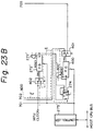
- Figures 23A and 23B are diagrams showing signal routes used when initially setting delay times in the
programmable delay circuits - Figures 24A and 24B are diagrams showing a signal route used in the delay time measuring & setting circuit 27k (k=1 to m) of the construction of Figs. 22A and 22B when measuring a time elapsing while a signal is propagated to a processor connected to one of the delay & switch circuits 25kr (r=1 to n, k=1 to m) in the same row as the delay time measuring & setting circuit 27k (k=1 to m) in the arrangement of Fig. 16;
- Figures 25A and 25B are diagrams showing a signal route used in the delay time measuring & setting circuit 27k (k=1 to m) of the construction of Figs. 22A and 22B when the delay time measuring & setting
circuit 27₁ in Fig. 16 measures a time elapsing while a signal is propagated to another delay time measuring & setting circuit 27k' (k'=2 to m) in the same column as the delay time measuring & settingcircuit 27₁ in the arrangement of Fig. 16; - Figures 26A and 26B are diagrams showing a signal route used in the delay time measuring & setting circuit 27k (k=2 to m-1) of the construction of Figs. 22A and 22B when the delay time measuring & setting
circuit 27₁ in Fig. 16 measures a time elapsing while a signal is propagated to another delay time measuring & setting circuit 27k' (k'=3 to m), where the shown delay time measuring & settingcircuit 27k is in a midway of the signal propagation path in the arrangement of Fig. 16; - Figures 27A and 27B are diagrams showing a signal route used in the delay time measuring & setting circuit 27k (k=2 to m) of the construction of Figs. 22A and 22B when the delay time measuring & setting
circuit 27₁ in Fig. 16 measures a time elapsing while a signal is propagated to the delay time measuring & settingcircuit 27k; and - Figures 28A and 28B are diagrams showing a signal route used in the delay time measuring & setting circuit 27k (k=2 to m) of the construction of Figs. 22A and 22B during a normal operation of the parallel data processing apparatus in the fifth embodiment, where the routes κ1 and κ2 are used by the delay time measuring & setting
circuit 27₁ in Fig. 16, and the routes λ1 and λ2 are used by the delay time measuring & setting circuit 27k (k=2 to m) in the arrangement of Fig. 16. - Before describing the preferred embodiment of the present invention, first the basic principles of the first to third aspects of the present invention are explained below.
- According to the first aspect of the present invention, first, the time which elapses while the signal propagates from the predetermined position to the corresponding data processing unit and then returns from the processor to the predetermined position through each pair of signal paths, is measured by the delay measuring unit. This can be realized by the provision of the plurality of pairs of signal paths where the pairs respectively corresponding to the plurality of data processing units, and the signal paths in each of the plurality of pairs are made symmetrical with regard to the electrical length for a signal propagation. Then, the delays caused by the variable delay unit in all of the signal paths of the plurality of pairs of signal paths are adjusted, based on results of measurement by the delay measuring unit so that times elapsing while the signal is propagated from the predetermined position to the plurality of data processing units through the respective signal paths of the plurality of pairs of signal paths for supplying the signal to the data processing units, are equal.
- According to the second aspect of the present invention, the above provision of the first aspect of the present invention is made for a predetermined one of the clock signal and the asynchronous request signal.
- According to the third aspect of the present invention, the above provision of the first aspect of the present invention is made for both the clock signal and the asynchronous request signal.
- Figure 1 is a block diagram showing a construction of the first embodiment of the present invention. In Fig. 1,
reference numeral 1 denotes a host processor, 2 denotes a parallel data processing apparatus, 3₁, 3₂, ... 3n each denote a processor, 4 denotes a clock generator, 5 denotes a request reception circuit, 6a₁, 6a₂, ... 6an each denote a programmable delay circuit, 7a denotes a delay time measuring & setting circuit, 9a₁, 9a₂, ... 9an each denote a selector, 10a₁, 10a₂, ... 10an each denote a programmable delay circuit, 11a₁, 11a₂, ... 11an each denote a selector, 12a₂ denotes an offset adjusting circuit, 13a and 13a' each denote a waveform shaping circuit, 14a denotes an offset adjusting circuit, 15 denotes a clock signal supply path, 16 denotes a return path corresponding to the clocksignal supply path return path 16. - The construction of Fig. 1 is an embodiment of the above-mentioned second aspect of the present invention. In the construction of Fig. 1, the clock
signal supply path 15 and thereturn path 16 are provided along the plurality ofprocessors signal supply path 15 and thereturn path 16 is connected with theclock generator 4. Further, all other designs in the clocksignal supply path 15 and thecorresponding return path 16 are made symmetrical with regard to a signal propagation. The clocksignal supply path 15 has a branch path 33a₁, 33a₂, ... 33an for each of the plurality ofprocessors signal supply path 15 with a clock input terminal of the corresponding processor. Thereturn path 16 has a branch path 34a₁, 34a₂, ... 34an for each of the plurality ofprocessors return path 16 with the clock input terminal of the corresponding processor. All other designs in the above corresponding branch paths 33a₁, 33a₂, ... 33an and 34a₁, 34a₂, ... 34an are made symmetrical with regard to a signal propagation. One of the programmable delay circuits (variable delay circuits) 6a₁, 6a₂, ... 6an is provided on a corresponding one of the branch paths 33a₁, 33a₂, ... 33an, and one of the programmable delay circuits (variable delay circuits) 10a₁, 10a₂, ... 10an is provided on a corresponding one of the branch paths 34a₁, 34a₂, ... 34an. Thereturn path 16 comprises thereon the plurality of selectors 9a₁, 9a₂, ... 9an. Each of the selectors 9a₁, 9a₂, ... 9an-1 connects at its two input terminals the upstream side of thereturn path 16 and a corresponding one of the branch paths 10a₁, 10a₂, ... 10an, and connects at its output terminal the downstream side of thereturn path 16. In order o symmetrize a path of a signal from theclock generator 4 to the clock input terminal of each processor and a path of the signal from the clock input terminal of the processor to theclock generator 4, the selectors 11a₁, 11a₂, ... 11an are provided on the clocksignal supply path 15 at the locations corresponding to the locations of the selectors 9a₁, 9a₂, ... 9an on thereturn path 16. - Each of the clock
signal supply path 15 and thereturn path 16 comprises awaveform shaping circuit waveform shaping circuits signal supply path 15 and thereturn path 16 are provided in correspondence to each other. The offset adjustingcircuit 14a is provided for the correspondingwaveform shaping circuits waveform shaping circuits waveform shaping circuits - An input terminal of the delay time measuring & setting
circuit 7a is connected to the clocksignal supply path 15 at the clock output terminal of theclock generator 4, and a clock output terminal of the delay time measuring & settingcircuit 7a is connected to thereturn path 16 at the clock input terminal of theclock generator 4. - In the above construction for supplying the clock signal to the
processors waveform shaping circuits circuit 7a to a clock input terminal of a corresponding processor and a corresponding path for returning the clock input terminal of the corresponding processor to the input terminal of the delay time measuring & settingcircuit 7a. Then, the delay time measuring & settingcircuit 7a measures a propagation delay time for a signal to be propagated from the delay time measuring & settingcircuit 7a to the clock input terminal of each processor and then propagated from the clock input terminal of the processor to the delay time measuring & settingcircuit 7a. Then, the delay time measuring & settingcircuit 7a obtains a propagation delay time for a signal to be propagated from the delay time measuring & settingcircuit 7a to the clock input terminal of each processor by dividing the above measured time by two, taking advantage of the above symmetricallity of the paths between the delay time measuring & settingcircuit 7a and each processor. After obtaining the propagation delay times for all of the plurality ofprocessors circuit 7a sets an additional delay time in the corresponding one of the programmable delay circuits 6a₁, 6a₂, ... 6an on the corresponding one of the branch paths 33a₁, 33a₂, ... 33an to each processor so that propagation delay times from the clock output terminal of theclock generator 4 to the input terminals of the plurality ofprocessors programmable delay circuits 253 in the delay & switch circuit 25r (r=1 to n). The above additional time for each programmable delay circuit can be determined as a difference between the maximum of the above obtained propagation delay times to the processors and the obtained propagation delay time to the corresponding processor, as shown in Fig. 2. Thus, an initial setting of the paralleldata processing apparatus 2 of Fig. 1 is completed. - In the operation of the parallel
data processing apparatus 2 of Fig. 1, therequest reception circuit 5 receives an asynchronous request signal supplied from thehost processor 1. The asynchronous request signal is, for example, an interrupt signal, or a hold request signal. When receiving the asynchronous request signal, therequest reception circuit 5 sends a clock frequency down control signal to theclock generator 4 to temporarily lower the frequency of the clock signal output from theclock generator 4. - The
clock generator 4 comprises an oscillator, a frequency divider, and a frequency division rate control circuit for controlling a frequency division rate of the frequency divider. When theclock generator 4 receives the above clock frequency down control signal, the frequency division rate control circuit temporarily lowers the frequency of the clock signal. Then, the frequency division rate control circuit sends a complete signal, which indicates a completion of the lowering operation of the frequency of the clock signal, to therequest reception circuit 5. Upon receiving the complete signal, therequest reception circuit 5 sends the asynchronous request signal to the plurality ofprocessors request signal path 17. When each processor receives the asynchronous request signal, the processor returns an acknowledge signal to therequest reception circuit 5 through the acknowledgesignal path 18. When therequest reception circuit 5 receives the acknowledge signal, therequest reception circuit 5 sends a clock frequency up control signal to theclock generator 4. Upon receiving the clock frequency up control signal, the frequency division rate control circuit temporarily increases the frequency of the clock signal to a predetermined frequency used in a normal operation. Namely, the above reception of the asynchronous request signal by each processor is carried out while the frequency of the clock signal supplied to the processor is lowered, i.e., the clock cycle is lengthened (for example, anormal cycle 30 nsec is increased to 240 nsec), and therefore, the operations in therespective processors - In the above construction, the above asynchronous
request signal path 17 to the plurality ofprocessors - Figure 3 is a block diagram showing a construction of the second embodiment of the present invention. In Fig. 3, reference numeral 2' denotes a parallel data processing apparatus, 5' denotes a request reception circuit, 6b₁, 6b₂, ... 6bn each denote a programmable delay circuit, 7b denotes a delay time measuring & setting circuit, 9b₁, 9b₂, ... 9bn each denote a selector, 10b₁, 10b₂, ... 10bn each denote a programmable delay circuit, 11b₁, 11b₂, ... 11bn each denote a selector, 12b₂ denotes an offset adjusting circuit, 13b and 13b' each denote a waveform shaping circuit, 14b denotes an offset adjusting circuit, 15 denotes a clock signal supply path, 16 denotes a clock signal return path, 17 denotes an asynchronous request signal path, 18 denotes an acknowledge signal path, 19 denotes an asynchronous request signal path, 20 denotes a return path corresponding to the asynchronous
request signal path return path 16. The other elements in Fig. 3 which are denoted by the same reference numerals as in Fig. 1, are respectively the same elements as shown in that figure. - The construction of Fig. 3 is an embodiment of the above-mentioned second aspect of the present invention. In the construction of Fig. 3, a provision for adjusting propagation delay times to the plurality of
processors - Similar to the construction of Fig. 1, the frequency of the clock signal is lowered when an asynchronous request signal is supplied to the plurality of
processors clock generator 4 responding to the reception of the asynchronous request signal from thehost processor 1 and the reception of the acknowledge signal from the processors. The request reception circuit 5' outputs the asynchronous request signal to the plurality ofprocessors clock generator 4, respectively. - Namely, the above reception of the asynchronous request signal by each processor is carried out while the frequency of the clock signal supplied to the processor is lowered, i.e., the clock cycle is lengthened, and therefore, the operations in the
respective processors - In the above construction, the above clock
signal supply path 21 to the plurality ofprocessors - Figure 4 is a block diagram showing a construction of the third embodiment of the present invention. In Fig. 4, reference numeral 2'' denotes a parallel data processing apparatus, and 5'' denotes a request reception circuit. The other elements in Fig. 4, which are denoted by the same reference numerals as Figs. 1 and 2, are respectively the same elements as shown in these figures.
- The construction of Fig. 4 is an embodiment of the above-mentioned third aspect of the present invention. In the construction of Fig. 4, the provision for adjusting propagation delay times to the plurality of
processors - In the construction of Fig. 4, however, no provision is made for lowering the frequency of the clock signal, as since both the asynchronous request signal and the clock signal are respectively supplied to the plurality of
processors - Figure 5 is a block diagram showing a construction of the fourth embodiment of the present invention. In Fig. 5, reference numeral 1' denotes a host processor, 200 denotes a parallel data processing apparatus, 22₁, 22₂, ... 22n each denote a processor, 23 denotes an MPU clock generator, 24 denotes a request reception & clock control circuit, 25₁, 25₂, ... 25n each denote a delay & switch circuit, 27 denotes a delay time measuring & setting circuit, 28 denotes a control bus, 29 denotes an asynchronous request signal path, 30 denotes an acknowledge signal path, 31 denotes a clock signal supply path, and 32 denotes a return path corresponding to the clock
signal supply path 31. The delay & switchcircuits processors circuit 27. - The construction of Fig. 5 is an embodiment of the above-mentioned second aspect of the present invention, and is basically similar to the construction of Fig. 1. The function for supplying the clock signal to the plurality of
processors circuits circuit 27. Details of each of the delay & switchcircuits circuit 27 will be explained later. - Figure 6 is a block diagram showing a construction of the
MPU clock generator 23 in the construction of Fig. 5. In Fig. 6,reference numeral 230 denotes a controller, 231 denotes a frequency division rate counter, and 232 denotes a frequency divider. - The
controller 230 receives an up/down control signal supplied from the request reception &clock control circuit 24, and outputs an up/down signal U/D to the frequencydivision rate counter 231 according to the received up/down control signal. Figure 7 is a state transition diagram of the frequencydivision rate counter 231 in the construction of Fig. 6. The frequencydivision rate counter 231 is initially in the state "S7", where the frequencydivision rate counter 231 outputs a count equal to seven. When the state of the frequencydivision rate counter 231 is in the state "S7" and the above U/D signal indicates a count down, i.e., U/D=0, the state of the frequencydivision rate counter 231 remains in the state "S7". When the state of the frequencydivision rate counter 231 is in the state "S7" and the above U/D signal indicates an instruction to increase the count by one, i.e., U/D=1, the state of the frequencydivision rate counter 231 is shifted one state by one state from the state "S7" to the state "S0", as "S7"→"S6", "S6"→"S5", ... "S1"→"S0", where the frequencydivision rate counter 231 outputs a count equal to i in the state "Si" (r=0 to 7). In the state "S0", the frequencydivision rate counter 231 outputs a COMPLETE signal to the request reception &clock control circuit 24. When the state of the frequencydivision rate counter 231 is in the state "S0" and the above U/D signal indicates a count down, i.e., U/D=0, the state of the frequencydivision rate counter 231 remains in the state "S0". When the state of the frequencydivision rate counter 231 is in the state "S0" and the above U/D signal indicates a count up, i.e., U/D=1, the state of the frequencydivision rate counter 231 is shifted one state by one state from the state "S0" to the state "S7", as "S0"→"S1", "S1"→"S2", ... "S6"→"S7". - Figure 8 is a state transition diagram of the
frequency divider 232 in the construction of Fig. 6. Thefrequency divider 232 is realized by a counter in which the count is increased by one when a leading edge of a master clock signal is supplied thereto from a master oscillator (not shown). In Fig. 8, "Ci" denotes a state of the counter which outputs a count equal to i, where r=0 to 7. As shown in Fig. 8, in the state "Si" of the frequencydivision rate counter 231, the count of the counter is cyclically changed from 0 to i, and a carry signal is output when the count reaches i. When the state of the frequencydivision rate counter 231 is "S0", thefrequency divider 232 outputs an MPU clock signal having a frequency which is the same as the frequency of the master clock signal. Namely, the frequency division rate in thefrequency divider 232 is equal to i+1. - Figure 9 is a state transition diagram of the request reception &
clock control circuit 24 in the construction of Fig. 5. The request reception &clock control circuit 24 is in an initial state "Init" after power is made ON. When an inactive master reset signal
clock control circuit 24 which is in the initial state, from the host processor 1', the state of the request reception & clock control circuit transits to a state ST1. When the request reception &clock control circuit 24 in the state "ST1" receives an active start signal START=1, the state of the request reception &clock control circuit 24 transits to the state "ST2". In the state "ST2", the request reception &clock control circuit 24 outputs an active U/D signal U/D=1 to theMPU clock generator 23, and waits for an asynchronous request signal from the host processor 1'. When the request reception &clock control circuit 24 in the state "ST2" receives an active asynchronous request (interrupt request) signal (
clock control circuit 24 transits to the state "ST1", and outputs an inactive U/D signal U/D=0 to theMPU clock generator 23 to lower the frequency of the MPU clock signal. When the request reception &clock control circuit 24 receives an active complete signal COMPLETE=1 from theMPU clock generator 23, and then receives an active acknowledge signal IACK=1, the request reception &clock control circuit 24 transits to the state "ST2". When an active master reset signal
clock control circuit 24 from the host processor 1', the request reception &clock control circuit 24 transits to the initial state "Init". The timing of an example operation of theMPU clock generator 23 of Fig. 6 is shown in Fig. 10. - Although not shown, generally, a plurality of paths for supplying a plurality of asynchronous request signals to the processors and a plurality of paths for returning a plurality of acknowledge signals corresponding to the plurality of asynchronous request signals to the request reception &
clock control circuit 24 are provided. The plurality of asynchronous request signals may include interrupt signals of a plurality of priority levels, and a hold request signal. Figure 11 is a diagram showing an example sequence in reception of an interrupt request signal by the paralleldata processing apparatus 200 in Fig. 5. - When the host processor 1' sends an interrupt request to the parallel
data processing apparatus 200, the request reception &clock control circuit 24 starts the above-mentioned operation for lowering the frequency of the MPU clock signal. When the operation is completed, the request reception &clock control circuit 24 outputs a LOW SPEED INDICATION to the host processor 1', and outputs an interrupt request signal to the plurality ofprocessors processors 
clock control circuit 24, and the operations according to the interrupt signal are commenced in the respective processors. Upon receiving the active interrupt acknowledge signal
clock control circuit 24 sends an INTERUPT ACKNOWLEDGE INDICATION to the host processor 1', and starts the above-mentioned operation for increasing the frequency of the MPU clock signal to the frequency of the master clock signal. When the operation is completed, the request reception &clock control circuit 24 sends a HIGH SPEED INDICATION to the host processor 1'. - Figure 12 is a diagram showing an example sequence in reception of a hold request signal by the parallel
data processing apparatus 200 in Fig. 5. - When the host processor 1' sends a hold request to the parallel
data processing apparatus 200, the request reception &clock control circuit 24 starts the above-mentioned operation for lowering the frequency of the MPU clock signal. When the operation is completed, the request reception &clock control circuit 24 outputs a LOW SPEED INDICATION to the host processor 1', and outputs a hold signal to the plurality ofprocessors processors 
clock control circuit 24, and theprocessors 
clock control circuit 24 sends a HOLD COMPLETE INDICATION to the host processor 1'. When receiving the HOLD COMPLETE INDICATION, the host processor 1' sends a release request signal to the request reception &clock control circuit 24, and the release request signal is transferred to theprocessors processors 
clock control circuit 24, and theprocessors 
clock control circuit 24 starts the above-mentioned operation for increasing the frequency of the MPU clock signal to the frequency of the master clock signal, and when the operation is completed, the request reception &clock control circuit 24 sends a HIGH SPEED INDICATION to the host processor 1'. - Figure 13 is a block diagram showing a construction of the delay & switch circuit 25r (r=1 to n) of Fig. 5. In Fig. 13,
reference numerals - The MPU clock signal is supplied from the delay time measuring & setting
circuit 27 or one of the delay & switchcircuits buffer amplifier 250 and theselector 251. Theselector 251 corresponds to one of the selectors 11a₁, 11a₂, ... 11an in Fig. 1. The output of theselector 251 is divided into two ways: a way to another (if any) of the delay & switchcircuits buffer amplifier 252 is provided on the way; and a way to a clock input terminal of the corresponding processor through the output port A, and theprogrammable delay circuit 253 and theselector 254 are provided on the way. The output of theselector 254 is further divided into two ways: the above way to the other of the delay & switchcircuits MPU clock generator 23. The loop-back way is connected with an input terminal of theselector 255. A timing signal output from the corresponding processor is applied to the other input terminal of theselector 255 through the input port B of the delay & switch circuit. The output of theselector 255 is applied to theprogrammable delay circuit 256, and the output of theprogrammable delay circuit 256 is applied to one of the input terminal of theselector 258. A signal returned toward theMPU clock generator 23 from the above other (if any) of the delay & switchcircuits buffer amplifier 257. The output of theselector 258 is output through thebuffer amplifier 259 and the output port D. As indicated in Fig. 13, thebuffer amplifier 257 is provided corresponding to thebuffer amplifier 252; theselector 255 is provided corresponding to theselector 254; theprogrammable delay circuit 256 is provided corresponding to theprogrammable delay circuit 253; theselector 258 is provided corresponding to theselector 251; and thebuffer amplifier 259 is provided corresponding to thebuffer amplifier 250; in order to make symmetrical the ways for supplying a signal to the downstream side and for returning the signal from the downstream side to the upstream side. The aboveprogrammable delay circuit 253 corresponds to one of the programmable delay circuits 6a₁, 6a₂, ... 6an in the construction of Fig. 1, and theprogrammable delay circuit 256 corresponds to one of the programmable delay circuits 10a₁, 10a₂, ... 10an in Fig. 1. The delay times in theprogrammable delay circuits control bus 28 in Fig. 5. Although the provision for initially adjusting the delay times in theprogrammable delay circuits - In some parallel data processing apparatuses, a timing signal output from each processor is used for processing data. This timing signal is generated in each processor responding to the MPU clock signal input thereto, for example, by frequency dividing the MPU clock signal. In this case, the times at which the above timing signals are output from all of the
processors selector 255 must select the signal from the input port B in the delay & switch circuit of Fig. 13 when the delay & switch circuit is connected to the processor for which the propagation delay time is to be measured. - Figure 14 is a block diagram showing an example construction of the
programmable delay circuit reference numeral 901 denotes aramp voltage generator 902 denotes a digital to analog converter, and 903 denotes a comparator. Theramp voltage generator 902 generates a ramp voltage when triggered by an input of a leading edge of the MPU clock signal. The ramp voltage increases with a predetermined rate from the time of the above input of the leading edge. The digital to analog converter is a multiplication type digital to analog converter, outputs an analog voltage proportional to a delay time value set thereto and used as a reference voltage in thecomparator 903. Thecomparator 903 compares the above ramp voltage with the above reference voltage. When the ramp voltage exceeds the reference voltage, the output of thecomparator 903 rises. Thus, the programmable delay circuit of Fig. 14 delays the MPU clock signal by an amount determined by the delay time value set in the digital to analog converter. - Since there is an offset in the output voltage of each of the digital to
analog converter 902 and theramp voltage generator 901, the delay time in the programmable delay circuit of Fig. 14 also has an offset. The provision for cancelling the affect of the above offset will be explained in the fifth embodiment of the present invention. - Figure 15 is a block diagram showing an example construction of the delay time measuring & setting
circuit 27 in the construction of Fig. 5. In Fig. 13,reference numerals - A signal supplied from the
MPU clock generator 23 is amplified through thebuffer amplifier 270, and the output of thebuffer amplifier 270 is divided into two ways: a way to the first delay & switchcircuits 25₁ through the output port H, and thebuffer amplifier 271 is provided on the way; and a way to an edge-triggered input terminal of the D-type flip-flop circuit 274. A signal input from the input port I is applied to the data input terminal of the D-type flip-flop circuit 274 through thebuffer amplifier 273, and the Q output of the D-type flip-flop circuit 274 is monitored by thecontroller 275. - Although the provision for initially adjusting the delay times in the
programmable delay circuit 272 is not indicated in Fig. 15, this provision is explained in the fifth embodiment. - After the above initial adjusting operation is completed, the
controller 275 controls theselectors 258 in the delay & switchcircuits selector 254 in one of the delay & switchcircuits circuit 27, where the delay & switch circuit at which the signal is loop-backed is connected to a processor at which the propagation delay time from the delay &switch circuit 27 is to be measured. Then, the delay &switch circuit 27 causes the master clock generator (not shown) to output a single timing pulse having a predetermined width when measuring the aforementioned propagation delay time. This operation is carried out in response to a command from the host processor 1' through the host CPU bus. The Q output of the D-type flip-flop circuit 274 becomes "1" when the timing of the input of the above single timing pulse into the edge-triggered input terminal of the flip-flop circuit 274 and the timing of the input of the above single timing pulse into the D input of the flip-flop circuit 274 coincide. Namely, the Q output of the D-type flip-flop circuit 274 becomes "1" when the delay time caused by theprogrammable delay circuit 272 coincides with the propagation delay time of the signal output from the output port H and then returned through the input port I. Therefore, the propagation delay time can be measured by scanning the delay time set in theprogrammable delay circuit 272 to find the delay time value which makes the Q output of the flip-flop circuit 274 "1". As explained before, the above measurement is carried out for all of theprocessors - Figure 16 is a block diagram showing an arrangement of a plurality of the delay time measuring & setting circuit 27k (k=1 to m) and the delay & switch circuit 25kr (r=1 to n, k=1 to m) in the fifth embodiment of the present invention. As shown later in Figs. 17A and 17B, processors similar to the
processors - As shown in Fig. 16, the delay time measuring & setting circuits 25kr (r=1 to n, k=1 to m) are arrayed in an n×m matrix arrangement. Each of the plurality of delay time measuring & setting circuits 27k (k=1 to m) is connected to the delay & switch circuit 25kr (r=1 to n, k=1 to m) which are arrayed on the j-th row. The delay & switch circuit 25kr (r=1 to n, k=1 to m) on each row are chain connected to the corresponding delay time measuring & setting
circuit 27k as the delay time measuring & settingcircuit - Each of the delay time measuring & setting circuits 27k (k=1 to m) measures propagation delay times to the respective processors in the respective delay & switch circuit 25kr (r=1 to n, k=1 to m) on the same row as the delay time measuring & setting
circuits 27k. Then, the delay time measuring & settingcircuits 27₁ measures propagation delay times to the respective delay time measuring & setting circuits 27k (k=2 to m). The above delay times, which are measured in the respective delay time measuring & setting circuits 27k (k=2 to m), are transferred from controllers 275' (explained later with reference to Figs. 17A, 17B, 22A, and 22B) in the respective delay time measuring & setting circuits 27k (k=2 to m) to the controller in the delay time measuring & settingcircuits 27₁. Thus, the delay time measuring & settingcircuits 27₁ can obtain propagation delay times to the respective processors in the respective delay & switch circuit 25kr (r=1 to n, k=1 to m) on the n×m matrix. Then, the controller 275' in the delay time measuring & settingcircuit 27₁ sets the delay times in the programmable delay circuits on the routes for supplying the MPU clock signal to the processors in all of the delay & switch circuits 25kr (r=1 to n, k=1 to m) in a way similar to that explained, so that the MPU clock signal simultaneously reaches the clock input terminal of the processors in all of the delay & switch circuits 25kr (r=1 to n, k=1 to m). - In Fig. 16, references a, b, c, and d each denote an input or output port of the delay time measuring & setting circuit 27k (k=1 to m), and e, f, g, h, i, and j each denote an input or output port of the delay & switch circuit 25kr (r=1 to n, k=1 to m). In each delay & switch circuit, the MPU clock signal is supplied to the input port a from the corresponding delay time measuring & setting circuit 27k (k=1 to m) or another delay & switch circuit on the upstream side. The MPU clock signal is supplied from the output port c to another delay & switch circuit on the downstream side. The signal returning from the downstream side is input to the delay & switch circuit from the input port d, and the signal returning to the next delay & switch circuit is output from the output port b.
- The MPU clock signal supplied to the delay & switch circuit 25k1 (k=1 to m) is output from the output port f of each delay time measuring & setting circuit. The MPU clock signal returned from the delay & switch circuit 25k1 (k=1 to m) is input from the input port g of each delay time measuring & setting circuit. The MPU clock signal supplied to the delay time measuring & setting circuit 27k (k=2 to m) is output from the output port h of each delay time measuring & setting circuit 27k-1 (k=2 to m). The MPU clock signal returned from the delay time measuring & setting circuit 27k (k=2 to m) is input from the input port i of each delay time measuring & setting circuit 27k-1 (k=2 to m). The MPU clock signal supplied from the delay time measuring & setting circuit 27k (k=1 to m-1) is input from the input port e of each delay time measuring & setting circuit 27k+1 (k=1 to m-1). The MPU clock signal returned from each delay time measuring & setting circuit 27k (k=2 to m) is output from the output port j of the delay time measuring & setting circuit 27k (k=2 to m).
- Details of the delay & switch circuit 25kr (r=1 to n, k=1 to m) and the delay time measuring & setting circuits 27k (k=1 to m) and the operations of these circuits are explained below with reference to Figs. 17A to 28B.
- Figures 17A and 17B are diagrams showing the construction of the delay & switch circuit 25kr (r=1 to n, k=1 to m) in the construction of Fig. 16. In Figs. 17A and 17B,
reference numerals 22₁ to 22₄ each denote a processor, 250', 252', 257', and 259' each denote a buffer amplifier, 251', 252', 254₁ to 254₄, 255₁ to 255₄, 257', 258', 259', 300, 302, 307, 308, 309, and 312 each denote a selector, 253₁ to 253₄, 256', 304, and 305 each denote a programmable delay circuit, 275' denotes a controller, 301₁ to 301₄ and 306 each denote a D-type flip-flop circuit, 303₁ to 303₄ each denote a monostable multivibrator, 310₁ to 310₄ and 311₁ to 311₄ each denote a level converter, 314, 315, 353₁ to 353₄, and 356 each denote an OR circuit. - The
processors 22₁ to 22₄ are those to which the MPU clock signal is to be supplied, and theselector 300 is provided for selecting one of theprocessors 22₁ to 22₄ to measure the propagation delay time from the delay time measuring & settingcircuits 27₁ to the processor. Theprogrammable delay circuits 254₁ to 254₄ each correspond to theprogrammable delay circuit 253 in the construction of Fig. 13, and the programmable delay circuit 256' corresponds to theprogrammable delay circuit 256 in Fig. 13. The D-type flip-flop circuits 301₁ to 301₄ are provided for use in determining initial delay times in theprogrammable delay circuits 253₁ to 253₄. Theselector 302 is provided for selecting one of the routes to be used when initially adjusting the delay times in theprogrammable delay circuits 253₁ to 253₄, and a route to be used when measuring propagation delay times for therespective processors 22₁ to 22₄. - The
level converters 303₁ to 303₄ and 311₁ to 311₄ are provided on both sides of theprocessors 22₁ to 22₄ for converting signal levels between ECL circuitry and TTL circuitry. In this embodiment, the circuitry around theprocessors 22₁ to 22₄ is realized by the TTL circuitry, and the other circuitry for supplying the MPU clock signal to the processors is realized by the ECL circuitry. Themonostable multivibrators 303₁ to 303₄ are provided for supplying an asynchronous request signal having a predetermined duty ratio to theprocessors 22₁ to 22₄ when the circuitry of Figs. 17A and 17B is used for simultaneously supplying the asynchronous request signal to theprocessors 22₁ to 22₄ as in the second and third embodiments of Figs. 3 and 4. Theselectors 254₁ to 254₄ each correspond to theselector 254 in Fig. 13, and theselectors 255₁ to 255₄ each correspond to theselector 255 in Fig. 13. In each processor, X2 denotes an edge-triggered input terminal, and H1 denotes an output terminal for the aforementioned timing signal generated in the processor. - The
programmable delay circuit 304 and theOR circuit 314 constitute a waveform shaping circuit for shaping a signal which passes therethrough, and theprogrammable delay circuit 305 and theOR circuit 315 constitute a waveform shaping circuit for shaping a signal which passes therethrough. These waveform shaping circuits are respectively provided in the path for supplying the MPU clock signal and the path for returning the MPU clock signal toward theMPU clock generator 23 in order to make symmetrical these paths. The D-type flip-flop circuit 306 is provided for use in determining initial delay times in theprogrammable delay circuits circuit 314 receives the output of the correspondingprogrammable delay circuit 304, and a master reset signal which is supplied from the host processor 1', and the output of theOR circuit 314 is applied to a reset input terminal of theprogrammable delay circuit 304. The ORcircuit 315 receives the output of the correspondingprogrammable delay circuit 305, and the master reset signal, and the output of theOR circuit 315 is applied to a reset input terminal of theprogrammable delay circuit 305. The ORcircuits 353₁ to 353₄ are respectively connected to the correspondingprogrammable delay circuits 253₁ to 253₄ in a way similar to the above waveform shaping circuits for shaping waveforms of the signals passing therethrough. - The
selector 307 is provided for selecting one of a route to be used when initially adjusting delay times in theprogrammable delay circuits selector 308 is provided symmetricallity with theselector 300, and theselector 309 is provided for symmetricallity with theselector 302. - The above selectors, the programmable delay circuits, and the flip-flop circuits are controlled and monitored by the controller 275' in the delay time measuring & setting circuit 27k (k=1 to m).
- Figures 18A and 18B are diagrams showing signal routes used when initially setting delay times in the
programmable delay circuits 253₁ to 253₄ in the construction of Figs. 17A and 17B, for making symmetrical each pair of signal paths of the delay time measuring & setting circuit 27k (k=1 to m). In Figs. 18A and 18B, the above routes, respectively provided for initially setting delay times in theprogrammable delay circuits 253₁ to 253₄, are indicated by dashed lines along the corresponding signal lines in Figs. 17A and 17B. - When initially setting delay times in the
programmable delay circuits 253₁ to 253₄, the controller 275' controls the selectors in the construction of Figs. 17A and 17B so that the above indicated routes are realized. Then, the controller 275' causes the master clock generator (not shown) to output a single timing pulse having a predetermined width when measuring the aforementioned propagation delay time. This operation is carried out in response to a command from the host processor 1' through the host CPU bus. - A signal input into the input port a is applied through the buffer amplifier 250', the
selectors programmable delay circuits 253₁ to 253₄. The outputs of theprogrammable delay circuits 253₁ to 253₄ are respectively applied to the edge-triggered input terminal of the corresponding one of the flip-flop circuits 301₁ to 301₄. The output of theselector 308 is applied to one input terminal of theselector 302. The applied signal is selected and is output from theselector 302 to be applied to the edge-triggered input terminal of the programmable delay circuit 256'. The output of the programmable delay circuit 256' is applied to the D input terminal of the flip-flop circuits 301₁ to 301₄. The Q output of each of the D-type flip-flop circuits 301₁ to 301₄ becomes the "1" level when the timing of the input of the above single timing pulse into the edge-triggered input terminal of each flip-flop circuit and the timing of the input of the above single timing pulse into the D input of the flip-flop circuit coincide. Namely, the Q output of each D-type flip-flop circuit becomes "1" when the delay time caused by the correspondingprogrammable delay circuit 253r coincides with the propagation delay time of the signal which propagates through the programmable delay circuit 256'. Thus, the controller 275' initially sets in theprogrammable delay circuit 253r the delay time value which makes the Q output of the flip-flop circuit 253r "1". - Figures 19A and 19B are diagrams showing a signal route used when initially setting delay times in the
programmable delay circuits - The operation for initially setting delay times in the
programmable delay circuits programmable delay circuits 253₁ to 253₄. In the case of Figs. 19A and 19B, the single timing signal input through the input port a is applied through the buffer amplifier 250' and the selector 251' to the edge-triggered input terminal of theprogrammable delay circuit 304 and one input terminal of theselector 307. The above signal is selected by theselector 307 and applied to the edge-triggered input terminal of theprogrammable delay circuit 305. The output of theprogrammable delay circuit 305 is applied to the edge-triggered input terminal of the D-type flip-flop circuit 306. The above output of the selector 251' is also applied to the edge-triggered input terminal of theprogrammable delay circuit 304, and the output of theprogrammable delay circuit 304 is applied to the D input terminal of the flip-flop circuit 306. Thus, the controller 275' initially sets in theprogrammable delay circuit 304 the delay time value which makes the Q output of the flip-flop circuit 304 "1" when the above single timing pulse is input into the circuit of Figs. 19A and 19B. - Figures 20A and 20B are diagrams showing a signal route used when measuring a time elapsing while a signal is propagated to the
processor 22₁, in the delay time measuring & setting circuit 27k (k=1 to m) of the construction of Figs. 17A and 17B. - After the above initial adjusting operations are completed, the controller 275' controls the selectors in the construction of Figs. 17A and 17B so that the signal routes as indicated by dashed lines α, β, and γ are realized, where the route α is a signal route passing from the input port a to the output port c, the route β is a signal route passing from the input port d to the output port b, and the route γ is a signal route inputting from the input port a, loop-backing in the construction of Figs. 20A and 20B, and outputting from the output port b. The signal routes α passes through the buffer amplifier 250', the
selectors programmable delay circuit 253₁, thelevel converter 310₁, theselectors level converter 311₁, theselectors selector 258, and the buffer amplifier 259', the signal routes β passes through the buffer amplifier 250', the selector 251', theprogrammable delay circuit 304, theselector 312, and the buffer amplifier 252', and the signal route γ passes through the buffer amplifier 257', theselector 307, theprogrammable delay circuit 305, theselector 258, and the buffer amplifier 259'. The signal routes α and β are used when measuring the propagation delay time of a signal to one of the processors in the delay & switch circuit which is located on the downstream side of the construction of Figs. 20A and 20B, and the signal route γ is used when measuring the propagation delay time of a signal to one of the processors in the construction of Figs. 20A and 20B. - Figures 21A and 21B are diagrams showing signal routes used for supplying the MPU clock signal during a normal operation of the parallel data processing apparatus in the fifth embodiment, in the delay time measuring & setting circuit 27k (k=1 to m) of the construction of Figs. 17A and 17B.
- In Figs. 21A and 21B, δ1 denotes a signal route of the MPU clock signal to be supplied to a processor in the delay & switch circuit located on the downstream side the construction of Figs. 21A and 21B, and δ2 denotes a signal route of the MPU clock signal to be supplied to a
processor 22₁ in the construction of Figs. 21A and 21B. The signal route δ1 passes through the buffer amplifier 250', the selector 251', theprogrammable delay circuit 304, theselector 312, and the buffer amplifier 252', and the signal routes δ2 passes through the buffer amplifier 250', theselectors programmable delay circuit 253₁, thelevel converter 310₁, themonostable multivibrator 303₁, and theselectors 254₁. - Figures 22A and 22B are diagrams showing the construction of the delay time measuring & setting circuit 27k (k=1 to m) in the construction of Fig. 16. In Figs. 22A and 22B,
reference numerals - In the construction of Figs. 22A and 22B, the buffer amplifiers 271' and 273' respectively correspond to the
buffer amplifiers programmable delay circuit 272 in Fig. 15, the D-type flip-flop circuit 274' corresponds to the D-type flip-flop circuit 274 in Fig. 15, and the controller 275' corresponds to thecontroller 275 in Fig. 15. Theprogrammable delay circuit 400 is provided for initially adjusting a delay time in the programmable delay circuit 272' for compensating the aforementioned offset in the programmable delay circuit 272'. Theselector 401 is provided for selecting one of a route for use when initially adjusting the delay times in the programmable delay circuits 272', and a route for use when measuring the propagation delay times. Theselector 402 is provided for the symmetry with the provision of theselector 401. Theprogrammable delay circuit 403 is provided for adjusting a delay time in a path from the input port for the MPU clock signal or the input port e to the output port f. Theprogrammable delay circuit 404 is provided for initially adjusting a delay time in theprogrammable delay circuit 403. The D-type flip-flop circuit 405 is provided for use when determining initial delay times in theprogrammable delay circuits selector 406 is provided for selecting one of a route to be used when initially adjusting the delay times in theprogrammable delay circuits selector 407 is provided for selecting one of a route to be used when initially adjusting the delay times in theprogrammable delay circuits selector 408 is provided for the symmetry with the provision of theselector 406. Theselector 409 is provided symmetrically with theselector 407. Theprogrammable delay circuit 410 is provided for adjusting a delay time in a path from the input port for the MPU clock signal or the input port e to the output port h, and shaping a waveform of a signal passing therethrough. Theprogrammable delay circuit 411 is provided for adjusting a delay time in a path from the input port i to the output port j, and shaping a wave form of a signal passing therethrough. The D-type flip-flop circuit 412 is provided for determining initial delay times in theprogrammable delay circuits selector 413 is provided for selecting one of a route to be used when initially adjusting the delay times in theprogrammable delay circuits selector 414 is provided for the symmetry with the provision of theselector 413. Theselector 415 is provided for selecting one of a route to be used when measuring the propagation delay times to another delay time measuring & setting circuits below the construction of Figs. 22A and 22B, and a route to be used when measuring the propagation delay times to a processor in one of the delay & switch circuits which are arrayed on the same row as the delay time measuring & setting circuit of Figs. 22A and 22B. Theselector 416 is provided for selecting one of a route to be used for the MPU clock signal from the MPU clock input terminal of the construction of Figs. 22A and 22B, and a route to be used for the MPU clock signal supplied from the delay time measuring & setting circuit located above the construction of Figs. 22A and 22B. - The
programmable delay circuit 403 and theOR circuit 423, theprogrammable delay circuit 404 and theOR circuit 424, theprogrammable delay circuit 410 and theOR circuit 430, and theprogrammable delay circuit 411 and theOR circuit 431, respectively, function as a waveform shaping circuit for shaping a signal which passes therethrough. - The above selectors, the programmable delay circuits, and the flip-flop circuits are controlled and monitored by the controller 275' in the delay time measuring & setting circuit 27k (k=1 to m).
- Figures 23A and 23B are diagrams showing signal routes which are used when initially setting delay times in the
programmable delay circuits programmable delay circuits - When initially setting delay times in the
programmable delay circuits - The route ε is a signal route used when the initial delay times of the
programmable delay circuits 272' and 400 are determined to be set thereto. In this case, the initial delay times are set thereto so that a propagation delay time of a signal which passes through theselector 402 and the programmable delay circuit 272', and a propagation delay time of a signal which passes through theselector 401 and theprogrammable delay circuit 400 are the same. The initial delay times to be set are determined by the controller 275' by setting a certain delay time in one of theprogrammable delay circuits 272' and 400, scanning the delay time in the other of theprogrammable delay circuits 272' and 400, and monitoring the Q output of the D-type flip-flop circuit 274'. - The route ζ is a signal route used when the initial delay times of the
programmable delay circuits selector 409, theprogrammable delay circuit 403, and theselector 408, and a propagation delay time of a signal which passes through theselectors programmable delay circuit 404 are the same. The initial delay times to be set are determined by the controller 275' by setting a certain delay time in one of theprogrammable delay circuits programmable delay circuits flop circuit 405. - The route η is a signal route used when the initial delay times of the
programmable delay circuits programmable delay circuit 410 and theselector 414, and a propagation delay time of a signal which passes through theselector 413 and theprogrammable delay circuit 411 are the same. The initial delay times to be set are determined by the controller 275' by setting a certain delay time in one of theprogrammable delay circuits programmable delay circuits flop circuit 412. - Figures 24A and 24B are diagrams showing a signal route which is used in the delay time measuring & setting circuit 27k (k=1 to m) of the construction of Figs. 22A and 22B when measuring a time elapsing while a signal is propagated to a processor connected to one of the delay & switch circuits 25kr (r=1 to n, k=1 to m) in the same row as the delay time measuring & setting circuit 27k (k=1 to m) in the arrangement of Fig. 16. In Figs. 24A and 24B, the above routes are indicated by dashed lines along the corresponding signal lines in Figs. 22A and 22B.
- As shown in Figs. 24A and 24B, a signal input from the MPU clock input terminal, is propagated in two ways. Namely, the signal on the first way passes through the
selector 402 and the programmable delay circuit 272' to be applied to the edge-triggered input terminal of the flip-flop circuit 274', and the signal propagated on the second way passes through theselectors programmable delay circuit 403 and is output from the output port f to be propagated to a clock input terminal of an objective processor, to be loop-backed at the clock input terminal, and to be returned therefrom. The returned signal is then input from the input port g, and passes through theselector 407, theprogrammable delay circuit 404, theselector 401, and theprogrammable delay circuit 400 to be applied to the D input terminal of the flip-flop circuit 274'. Thus, the controller 275' can measure the propagation delay time value which makes the Q output of the flip-flop circuit 274' "1" when the above single timing pulse is input into the MPU clock input terminal of the circuit of Figs. 22A and 22B. - Figures 25A and 25B are diagrams showing a signal route used in the delay time measuring & setting circuit 27k (k=1 to m) of the construction of Figs. 22A and 22B when the delay time measuring & setting
circuit 27₁ in Fig. 16 measures a time elapsing while a signal is propagated to another delay time measuring & setting circuit 27k' (k'=2 to m) in the same column as the delay time measuring & settingcircuit 27₁ in the arrangement of Fig. 16. In Figs. 25A and 25B, the above routes are indicated by dashed lines along the corresponding signal lines in Figs. 22A and 22B. After the above initial adjusting operations are completed, the controller 275' controls the selectors in the construction of Figs. 22A and 22B so that the signal routes are as indicated by the dashed lines. - As shown in Figs. 25A and 25B, a signal input from the MPU clock input terminal, is propagated in two ways. The signal on the first way passes through the
selector 402 and the programmable delay circuit 272' to be applied to the edge-triggered input terminal of the flip-flop circuit 405, and the signal propagated on the second way passes through theprogrammable delay circuit 410 and theselector 414 and is output from the output port h to be propagated to a clock input terminal of an objective processor, to be loop-backed at the clock input terminal, and to be returned therefrom. The returned signal is then input from the input port i, and passes through theselector 413, theprogrammable delay circuit 411, theselector 415, theselector 401, and theprogrammable delay circuit 400 to be applied to the D input terminal of the flip-flop circuit 274'. Thus, the controller 275' can measure the propagation delay time value which makes the Q output of the flip-flop circuit 274' "1" when the above single timing pulse is input to the MPU clock input terminal of the circuit of Figs. 22A and 22B. - Figures 26A and 26B are diagrams showing a signal route used in the delay time measuring & setting circuit 27k (k=2 to m-1) of the construction of Figs. 22A and 22B when the delay time measuring & setting
circuit 27₁ in Fig. 16 measures a time elapsing while a signal is propagated to another delay time measuring & setting circuit 27k' (k'=3 to m), where the shown delay time measuring & settingcircuit 27k is midway the signal propagation path in the arrangement of Fig. 16. - After the above initial adjusting operations are completed, the controller 275' controls the selectors in the construction of Figs. 22A and 22B so that the signal routes as indicated by dashed lines ϑ and, are realized, where the route ϑ is a signal route passing from the input port e to the output port h, and the route
 is a signal route passing from the input port i to the output port j. The signal route ϑ passes through the
buffer amplifier 276, theselector 416, theprogrammable delay circuit 410, theselector 414, and thebuffer amplifier 277. The signal routepasses through thebuffer amplifier 278, theselector 413, theprogrammable delay circuit 411, theselector 415, and thebuffer amplifier 279. - Figures 27A and 27B are diagrams showing a signal route used in the delay time measuring & setting circuit 27k (k=2 to m) of the construction of Figs. 22A and 22B when the delay time measuring & setting
circuit 27₁ in Fig. 16 measures a time elapsing while a signal is propagated to the delay time measuring & settingcircuit 27k. - After the above initial adjusting operations are completed, the controller 275' controls the selectors in the construction of Figs. 22A and 22B so that the signal route as indicated by a dashed line is realized, where the route ϑ is a signal route passing from the input port e to the output port h, and the routeis a signal route passing from the input port i to the output port j. The signal routes ϑ passes through the
buffer amplifier 276, theselectors programmable delay circuit 403, theselectors programmable delay circuit 404, theselector 415, and thebuffer amplifier 279. - Figures 28A and 28B are diagrams showing a signal route used in the delay time measuring & setting circuit 27k (k=2 to m) of the construction of Figs. 22A and 22B during a normal operation of the parallel data processing apparatus in the fifth embodiment, where the routes κ1 and κ2 are used by the delay time measuring & setting
circuit 27₁ in Fig. 16, and the routes λ1 and λ2 are used by the delay time measuring & setting circuit 27k (k=2 to m) in the arrangement of Fig. 16. - In Figs. 28A and 28B, the MPU clock signal input from the MPU clock input terminal of the delay time measuring & setting
circuit 27₁ passes through theselectors programmable delay circuit 403 and the buffer amplifier 271' (the route κ1), and is output from the output port f to the delay & switch circuits 251r (r=1 to n). In addition, the above MPU clock signal passes through theprogrammable delay circuit 410, theselector 414, and the buffer amplifier 277 (the route κ2), and is output from the output port h to the delay time measuring & setting circuits 27k (k=2 to m). In the other delay time measuring & setting circuits 27k (k=2 to m), the MPU clock signal supplied from one of the delay time measuring & setting circuit 27k-1 (k=2 to m) located above the delay time measuring & setting circuit 27k (k=2 to m), through the input port e and thebuffer amplifier 276. The MPU clock signal output from thebuffer amplifier 276 is propagated on the same ways (λ1 and λ2) as the above routes κ1 and κ2, respectively.
Claims (23)
- An apparatus for supplying a signal to a plurality of data processing units (3₁, 3₂, ... 3n), comprising:
a plurality of pairs of signal paths (15, 16, 33a₁, 33a₂, ... 33an, 34a₁, 34a₂ ... 34an), said pairs respectively correspond to said plurality of data processing units (3₁, 3₂, ... 3n), one signal path (15, 33a₁, 33a₂, ... 33an) of each of the plurality of pairs is provided for supplying said signal from a predetermined position which is common to all of the plurality of pairs of signal paths, to a corresponding data processing unit, the other signal path (16, 34a₁, 34a₂, ... 34an) of each of the plurality of pairs is provided for returning said signal from the corresponding data processing unit to said predetermined position, and the signal paths (15, 16, 33a₁, 33a₂, ... 33an, 34a₁, 34a₂, ... 34an) in each of the plurality of pairs are made symmetrical with regard to electrical length for a signal propagation, where each of said plurality of pairs of signal paths comprises variable delay means (6a₁, 6a₂, ... 6an, 10a₁, 10a₂, ... 10an) for delaying a propagation of a signal through the signal path;
delay measuring means (7a) for measuring time elapsing while said signal is propagated from said predetermined position to the corresponding data processing unit and then returned from the data processing unit to the predetermined position through each pair of signal paths; and
delay adjusting means (7a) for adjusting the delays caused by the variable delay means (6a₁, 6a₂, ... 6an, 10a₁, 10a₂, ... 10an) in all of the signal paths of the plurality of pairs of signal paths, based on results of measurement by the delay measuring means (7a), so that times which elapse while said signal propagates from said predetermined position to the plurality of data processing units through the respective signal paths (15, 33a₁, 33a₂, ... 33an) of the plurality of pairs of signal paths for supplying the signal to the data processing units, are equal. - A parallel data processing apparatus according to claim 1, further comprising initial symmetrical means (12a) for setting delays caused by the variable delay means in all of the signal paths of the plurality of pairs of signal paths before the operation of said delay adjusting means, so that the signal paths in each of the plurality of pairs cause the same delay in signal propagation.
- A parallel data processing apparatus comprising:
a plurality of processors (3₁, 3₂, ... 3n) for processing data in parallel, in synchronization with a common clock signal, and starting an operation thereof upon receiving a common asynchronous request signal;
clock generating means (4) for generating said common clock signal to said plurality of processors;
a plurality of pairs of signal paths (15, 16, 33a₁, 33a₂, ... 33an, 34a₁, 34a₂, ... 34an), said pairs respectively corresponding to said plurality of processors, one signal path (15, 33a₁, 33a₂, ... 33an) of each of the plurality of pairs being provided for supplying said predetermined one of said clock signal and said asynchronous request signal from a predetermined position common to all of the plurality of pairs of signal paths, to a corresponding processor, the other signal path (16, 34a₁, 34a₂, ... 34an) of each of the plurality of pairs being provided for returning said predetermined one of said clock signal and said asynchronous request signal from the corresponding processor to said predetermined position, and the signal paths (15, 16, 33a₁, 33a₂, ... 33an, 34a₁, 34a₂, ... 34an) in each of the plurality of pairs are made symmetrical with regard to an electrical length for a signal propagation, where each of said plurality of pairs of signal paths (33a₁, 33a₂, ... 33an) comprises a variable delay means (6a₁, 6a₂, ... 6an, 10a₁, 10a₂, ... 10an) for delaying a propagation of a predetermined one of said clock signal and said asynchronous request signal through the signal path;
a plurality of signal paths (17) for respectively supplying the other of said clock signal and said asynchronous request signal to said plurality of processors;
delay measuring means (7a) for measuring a time elapsing while said predetermined one of said clock signal and said asynchronous request signal are propagated from said predetermined position to the corresponding processor and then returned from the processor to the predetermined position through each pair of signal paths; and
delay adjusting means (7a) for adjusting the delays caused by the variable delay means in all of the signal paths of the plurality of pairs of signal paths, based on results of a measurement by the delay measuring means, so that times elapsing while said predetermined one of said clock signal and said asynchronous request signal are propagated from said predetermined position to the plurality of processors through the respective signal paths of the plurality of pairs of signal paths for supplying the predetermined one of said clock signal and said asynchronous request signal to the processors, are equal. - A parallel data processing apparatus according to claim 3, wherein said plurality of signal paths (17) are realized by equal-length wiring so that times elapsing while said other of said clock signal and said asynchronous request signal are propagated to the processors from a predetermined position common to all of the plurality of processors, to the processors, are equal.
- A parallel data processing apparatus according to claim 3 or 4, further comprising:
asynchronous request signal reception control means (24) for receiving the asynchronous request signal supplied from outside of said parallel data processing apparatus; and
clock frequency controlling means (23) for temporarily lowering a frequency of the clock signal when said asynchronous request signal reception control means receives the asynchronous request signal supplied from outside of said parallel data processing apparatus;
said asynchronous request signal reception control means (24) supplying said asynchronous request signal to all of the plurality of processors when the frequency of the clock signal is lowered to a predetermined frequency. - A parallel data processing apparatus according to any of claims 3 to 5, wherein all of the signal paths (15, 33a₁, 33a₂, ... 33an) for supplying said predetermined one of said clock signal and said asynchronous request signal to the plurality of processors share a common supply-side path (15), and each comprise branch means for branching the predetermined one of said clock signal and said asynchronous request signal from the common supply-side path to the corresponding processor, and a supply-side branch path (33a₁, 33a₂, ... 33an) for propagating said predetermined one of said clock signal and said asynchronous request signal, from the branch means to the corresponding processor, and
all of the signal paths (16, 34a₁, 34a₂, ... 34an) for returning said predetermined one of said clock signal and said asynchronous request signal from the plurality of processors share a common return-side path, and each comprise a return-side branch path (34a₁, 34a₂, ... 34an) for propagating said predetermined one of said clock signal and said asynchronous request signal from the corresponding processor to the common return-side path (16), and joining means (9a₁, 9a₂, ... 9an) for joining the return-side branch path to the common return-side path; and
said variable delay means (6a₁, 6a₂, ... 6an) is provided on each supply-side branch path. - A parallel data processing apparatus according to any of claims 3 to 6, wherein said plurality of processors (3₁, 3₂, ... 3n) are arranged in a predetermined order, said common return-side path (16) is arranged along the plurality of processors, and said joining means (9a₁, 9a₂, ... 9an) corresponding to each processor comprises a selector for receiving a signal propagated from said return-side branch path, and a signal propagated from said common return-side path of the upstream side, selecting one of the received signals, and outputting the selected signal onto the said common return-side path of the downstream side.
- A parallel data processing apparatus according to claim 6 or 7, further comprising variable delay means in each return-side branch path.
- A parallel data processing apparatus according to any of claims 3 to 8, further comprising initial symmetrical means (12a₁, 12a₂, ... 12an) for setting the delays caused by the variable delay means in all of the signal paths of the plurality of pairs of signal paths before the operation of said delay adjusting means, so that the signal paths in each of the plurality of pairs cause the same delay in signal propagation.
- A parallel data processing apparatus according to any of claims 6 to 9, further comprising variable delay means (10a₁, 10a₂, ... 10an) in said common return-side path.
- A parallel data processing apparatus according to claim 10, further comprising initial symmetrical means (12a₁, 12a₂, ... 12an) for initially setting delays caused by the variable delay means in all of the signal paths of the plurality of pairs of signal paths before the operation of said delay adjusting means, so that the signal paths in each of the plurality of pairs cause the same delay in signal propagation.
- A parallel data processing apparatus according to any of claims 3 to 11, further comprising waveform shaping means (2₁, 2₂, ... 2n) in each signal path of the plurality of pairs of signal paths.
- A parallel data processing apparatus according to claim 12, further comprising initial symmetrical means (14a) for initially adjusting the delays caused by the waveform shaping means in the signal paths in each pair of the plurality of pairs so that the signal paths in each of the plurality of pairs cause the same delay in signal propagation before the operation of said delay adjusting means.
- A parallel data processing apparatus comprising:
a plurality of processors (3₁, 3₂, ... 3n) for processing data in parallel, in synchronization with a common clock signal, and starting an operation thereof upon receiving a common asynchronous request signal;
clock generating means (4) for generating said common clock signal to said plurality of processors;
a first plurality of pairs of signal paths (15, 16, 33a₁, 33a₂, ... 33an, 34a₁, 34a₂, ... 34an), said pairs respectively corresponding to said plurality of processors, one signal path of each of the first plurality of pairs being provided for supplying said clock signal from a first predetermined position common to all of the first plurality of pairs of signal paths, to a corresponding processor, the other signal path of each of the first plurality of pairs being provided for returning said clock signal from the corresponding processor to said first predetermined position, and the signal paths in each of the first plurality of pairs are made symmetrical with regard to an electrical length for a signal propagation, where each of said first plurality of pairs of signal paths comprises first variable delay means (6a₁, 6a₂, ... 6an, 10a₁, 10a₂, ... 10an) for delaying a propagation of a clock signal through the signal path;
first delay measuring means (7a) for measuring a time elapsing while said clock signal is propagated from said first predetermined position to the corresponding processor and then returned from the processor to said first predetermined position through each pair of signal paths;
first delay adjusting means (7a) for adjusting the delays caused by the first variable delay means in all of the signal paths of the first plurality of pairs of signal paths, based on results of a measurement by the first delay measuring means, so that times elapsing while said clock signal is propagated from said first predetermined position to the plurality of processors through the respective signal paths of the first plurality of pairs of signal paths for supplying the clock signal to the processors, are equal;
a second plurality of pairs of signal paths (19, 20, 33b₁, 33b₂, ... 33bn, 34b₁, 34b₂, ... 34bn), said pairs respectively corresponding to said plurality of processors, one signal path (19, 33b₁, 33b₂, ... 33bn) of each of the second plurality of pairs being provided for supplying said asynchronous request signal from a second predetermined position common to all of the second plurality of pairs of signal paths to a corresponding processor, the other signal path (20, 34b₁, 34b₂, ... 34bn) of each of the second plurality of pairs being provided for returning said asynchronous request signal from the corresponding processor to said second predetermined position, and the signal paths in each of the second plurality of pairs are made symmetrical with regard to an electrical length for a signal propagation, where each of said second plurality of pairs of signal paths comprises second variable delay means for delaying a propagation of a asynchronous request signal through the signal path;
second delay measuring means (7b) for measuring a time elapsing while said asynchronous request signal is propagated from said second predetermined position to the corresponding processor and then returned from the processor to said second predetermined position through each pair of signal paths; and
second delay adjusting means (7b) for adjusting the delays caused by the second variable delay means in all of the signal paths of the second plurality of pairs of signal paths, based on results of a measurement by the second delay measuring means, so that times elapsing while said asynchronous request signal is propagated from said second predetermined position to the plurality of processors through the respective signal paths of the second plurality of pairs of signal paths for supplying the asynchronous request signal to the processors, are equal. - A parallel data processing apparatus according to claim 14, further comprising:
asynchronous request signal reception control means (24) for receiving the asynchronous request signal supplied from outside of said parallel data processing apparatus; and
clock frequency controlling means (23) for temporarily lowering a frequency of the clock signal when said asynchronous request signal reception control means receives the asynchronous request signal which is supplied from outside of said parallel data processing apparatus;
said asynchronous request signal reception control means (24) supplying said asynchronous request signal to all of the plurality of processors when the frequency of the clock signal is lowered to a predetermined frequency. - A parallel data processing apparatus according to claim 14 or 15, wherein all of the signal paths for supplying said clock signal to the plurality of processors share a first common supply-side path (15), and each comprise first branch means for branching the clock signal from the first common supply-side path to the corresponding processor, and a first supply-side branch path (33a₁, 33a₂, ... 33an) for propagating said clock signal, from the first branch means to the corresponding processor;
all of the signal paths for returning said clock signal from the plurality of processors share a first common return-side path (16), and each comprise a first return-side branch path (34a₁, 34a₂, ... 34an) for propagating said clock signal from the corresponding processor to the first common return-side path, and first joining means (9a₁, 9a₂, ... 9an) for joining the first return-side branch path to the first common return-side path;
all of the signal paths for supplying said asynchronous request signal to the plurality of processors share a second common supply-side path, and each comprise second branch means for branching said asynchronous request signal from the common supply-side path to the corresponding processor, and a second supply-side branch path for propagating said asynchronous request signal, from the second branch means to the corresponding processor;
all of the signal paths for returning said asynchronous request signal from the plurality of processors share a second common return-side path (20), and each comprise a second return-side branch path (34b₁, 34b₂, ... 34bn) for propagating said asynchronous request signal from the corresponding processor to the second common return-side path, and joining means (9b₁, 9b₂, ... 9bn) for joining the second return-side branch path to the second common return-side path; and
said variable delay means (6a₁, 6a₂, ... 6an, 6b₁, 6b₂, ... 6bn) being provided on each of the supply-side branch paths. - A parallel data processing apparatus according to claim 16, wherein said plurality of processors (3₁, 3₂, ... 3n) are arranged in a predetermined order, said first common return-side path (16) is arranged along the plurality of processors, and said first joining means (9a₁, 9a₂, ... 9an) corresponding to each processor comprises a selector for receiving a signal propagated from said first return-side branch path, and a signal propagated from said first common return-side path of the upstream side, selecting one of the received signals, and outputting the selected signal onto the said first common return-side path of the downstream side; and
said second common return-side path (20) is arranged along the plurality of processors, and said second joining means (9b₁, 9b₂, ... 9bn) corresponding to each processor comprises a selector for receiving a signal propagated from said second return-side branch path, and a signal propagated from said second common return-side path of the upstream side, selecting one of the received signals, and outputting the selected signal onto the said second common return-side path of the downstream side. - A parallel data processing apparatus according to claim 16 or 17, further comprising variable delay means (10a₁, 10a₂, ... 10an, 10b₁, 10b₂, ... 10bn) in each of the first and second return-side branch paths (34a₁, 34a₂, ... 34an, 34b₁, 34b₂, ... 34bn).
- A parallel data processing apparatus according to any of claims 14 to 18, further comprising initial symmetrical means (12a₁, 12a₂, ... 12an) for setting the delays caused by the variable delay means in all of the signal paths of the first and second plurality of pairs of signal paths before the operation of said first and second delay adjusting means, so that the signal paths in each of the first plurality of pairs cause the same delay in signal propagation, and the signal paths in each of the second plurality of pairs cause the same delay in signal propagation.
- A parallel data processing apparatus according to claim 16, further comprising variable delay means (10a₁, 10a₂, ... 10an, 10b₁, 10b₂, ... 10bn) in each of said first and second common return-side paths (34a₁, 34a₂, ... 34an, 34b₁, 34b₂, ... 34bn).
- A parallel data processing apparatus according to claim 20, further comprising initial symmetrical means (12a₁, 12a₂, ... 12an) for initially setting the delays caused by the variable delay means in all of the signal paths of the plurality of pairs of signal paths before the operation of said delay adjusting means, so that the signal paths in each of the plurality of pairs cause the same delay in signal propagation.
- A parallel data processing apparatus according to any of claims 14 to 21, further comprising waveform shaping means (13a, 13a', 13b, 13b') in each signal path of the first and second plurality of pairs of signal paths.
- A parallel data processing apparatus according to claim 22, further comprising initial symmetrical means (14a) for initially adjusting the delays caused by the waveform shaping means in the signal paths in each pair of the first and second plurality of pairs so that the signal paths in each of the first plurality of pairs cause the same delay in signal propagation, and the signal paths in each of the second plurality of pairs cause the same delay in signal propagation before the respective operations of said first and second delay adjusting means.
Applications Claiming Priority (3)
| Application Number | Priority Date | Filing Date | Title |
|---|---|---|---|
| JP2171069A JP2507677B2 (en) | 1990-06-28 | 1990-06-28 | Distributed data processor |
| JP171069/90 | 1990-06-28 | ||
| JP17106990 | 1990-06-28 |
Publications (3)
| Publication Number | Publication Date |
|---|---|
| EP0464632A2 true EP0464632A2 (en) | 1992-01-08 |
| EP0464632A3 EP0464632A3 (en) | 1993-08-25 |
| EP0464632B1 EP0464632B1 (en) | 1999-12-08 |
Family
ID=15916461
Family Applications (1)
| Application Number | Title | Priority Date | Filing Date |
|---|---|---|---|
| EP91110561A Expired - Lifetime EP0464632B1 (en) | 1990-06-28 | 1991-06-26 | Parallel data processing apparatus and method with signal skew compensation |
Country Status (6)
| Country | Link |
|---|---|
| US (1) | US5220660A (en) |
| EP (1) | EP0464632B1 (en) |
| JP (1) | JP2507677B2 (en) |
| AU (1) | AU636768B2 (en) |
| DE (1) | DE69131822T2 (en) |
| FI (1) | FI913114A (en) |
Families Citing this family (27)
| Publication number | Priority date | Publication date | Assignee | Title |
|---|---|---|---|---|
| US5577214A (en) * | 1992-05-18 | 1996-11-19 | Opti, Inc. | Programmable hold delay |
| US5572722A (en) * | 1992-05-28 | 1996-11-05 | Texas Instruments Incorporated | Time skewing arrangement for operating random access memory in synchronism with a data processor |
| JPH0793386A (en) * | 1993-09-28 | 1995-04-07 | Fujitsu Ltd | Lsi package designing system |
| US5467465A (en) * | 1993-11-17 | 1995-11-14 | Umax Data System Inc. | Two clock method for synchronizing a plurality of identical processors connected in parallel |
| JPH07248847A (en) * | 1994-03-11 | 1995-09-26 | Fujitsu Ltd | Method and device for adjusting clock signal |
| US5768620A (en) * | 1996-04-09 | 1998-06-16 | International Business Machines Corporation | Variable timeout method in a missing-interrupt-handler for I/O requests issued by the same operating system |
| US6115769A (en) * | 1996-06-28 | 2000-09-05 | Lsi Logic Corporation | Method and apparatus for providing precise circuit delays |
| US6557066B1 (en) | 1999-05-25 | 2003-04-29 | Lsi Logic Corporation | Method and apparatus for data dependent, dual level output driver |
| US6294937B1 (en) | 1999-05-25 | 2001-09-25 | Lsi Logic Corporation | Method and apparatus for self correcting parallel I/O circuitry |
| DE10006236C2 (en) * | 2000-02-11 | 2001-12-20 | Infineon Technologies Ag | Arrangement for generating signal pulses with defined pulse lengths in a module with a BIST function |
| JP3628265B2 (en) * | 2001-02-21 | 2005-03-09 | 株式会社半導体理工学研究センター | Multiprocessor system unit |
| KR100414943B1 (en) * | 2001-12-28 | 2004-01-16 | 엘지전자 주식회사 | Apparatus and Method for Distribution Clock in Multiple Processing System based on Compact Peripheral Component Interconnect |
| US7043649B2 (en) * | 2002-11-20 | 2006-05-09 | Portalplayer, Inc. | System clock power management for chips with multiple processing modules |
| US7698490B2 (en) * | 2005-12-21 | 2010-04-13 | Nvidia Corporation | Passive USB power configuration switching |
| US7414550B1 (en) | 2006-06-30 | 2008-08-19 | Nvidia Corporation | Methods and systems for sample rate conversion and sample clock synchronization |
| US9209792B1 (en) | 2007-08-15 | 2015-12-08 | Nvidia Corporation | Clock selection system and method |
| US9088176B2 (en) * | 2007-12-17 | 2015-07-21 | Nvidia Corporation | Power management efficiency using DC-DC and linear regulators in conjunction |
| US8327173B2 (en) * | 2007-12-17 | 2012-12-04 | Nvidia Corporation | Integrated circuit device core power down independent of peripheral device operation |
| US9411390B2 (en) | 2008-02-11 | 2016-08-09 | Nvidia Corporation | Integrated circuit device having power domains and partitions based on use case power optimization |
| US9423846B2 (en) | 2008-04-10 | 2016-08-23 | Nvidia Corporation | Powered ring to maintain IO state independent of the core of an integrated circuit device |
| US8762759B2 (en) * | 2008-04-10 | 2014-06-24 | Nvidia Corporation | Responding to interrupts while in a reduced power state |
| JP5604799B2 (en) * | 2009-03-06 | 2014-10-15 | 日本電気株式会社 | Fault tolerant computer |
| JP5800752B2 (en) * | 2012-04-25 | 2015-10-28 | 三菱電機株式会社 | Signal source synchronization circuit |
| US9395799B2 (en) | 2012-08-09 | 2016-07-19 | Nvidia Corporation | Power management techniques for USB interfaces |
| US9471395B2 (en) | 2012-08-23 | 2016-10-18 | Nvidia Corporation | Processor cluster migration techniques |
| US20140062561A1 (en) | 2012-09-05 | 2014-03-06 | Nvidia Corporation | Schmitt receiver systems and methods for high-voltage input signals |
| EP2775655B1 (en) * | 2013-03-08 | 2020-10-28 | Pro Design Electronic GmbH | Method of distributing a clock signal, a clock distributing system and an electronic system comprising a clock distributing system |
Citations (3)
| Publication number | Priority date | Publication date | Assignee | Title |
|---|---|---|---|---|
| US4063308A (en) * | 1975-06-27 | 1977-12-13 | International Business Machines Corporation | Automatic clock tuning and measuring system for LSI computers |
| US4847516A (en) * | 1986-11-26 | 1989-07-11 | Hitachi, Ltd. | System for feeding clock signals |
| US4868522A (en) * | 1988-12-13 | 1989-09-19 | Gazelle Microcircuits, Inc. | Clock signal distribution device |
Family Cites Families (4)
| Publication number | Priority date | Publication date | Assignee | Title |
|---|---|---|---|---|
| US4769558A (en) * | 1986-07-09 | 1988-09-06 | Eta Systems, Inc. | Integrated circuit clock bus layout delay system |
| US4805196A (en) * | 1987-04-29 | 1989-02-14 | Gte Laboratories Incorporated | Line delay compensation for digital transmission systems utilizing low power line drivers |
| US5086500A (en) * | 1987-08-07 | 1992-02-04 | Tektronix, Inc. | Synchronized system by adjusting independently clock signals arriving at a plurality of integrated circuits |
| US5041966A (en) * | 1987-10-06 | 1991-08-20 | Nec Corporation | Partially distributed method for clock synchronization |
-
1990
- 1990-06-28 JP JP2171069A patent/JP2507677B2/en not_active Expired - Fee Related
-
1991
- 1991-06-25 AU AU79273/91A patent/AU636768B2/en not_active Ceased
- 1991-06-26 FI FI913114A patent/FI913114A/en unknown
- 1991-06-26 DE DE69131822T patent/DE69131822T2/en not_active Expired - Fee Related
- 1991-06-26 EP EP91110561A patent/EP0464632B1/en not_active Expired - Lifetime
- 1991-06-27 US US07/722,198 patent/US5220660A/en not_active Expired - Lifetime
Patent Citations (3)
| Publication number | Priority date | Publication date | Assignee | Title |
|---|---|---|---|---|
| US4063308A (en) * | 1975-06-27 | 1977-12-13 | International Business Machines Corporation | Automatic clock tuning and measuring system for LSI computers |
| US4847516A (en) * | 1986-11-26 | 1989-07-11 | Hitachi, Ltd. | System for feeding clock signals |
| US4868522A (en) * | 1988-12-13 | 1989-09-19 | Gazelle Microcircuits, Inc. | Clock signal distribution device |
Also Published As
| Publication number | Publication date |
|---|---|
| EP0464632B1 (en) | 1999-12-08 |
| DE69131822D1 (en) | 2000-01-13 |
| US5220660A (en) | 1993-06-15 |
| DE69131822T2 (en) | 2000-04-06 |
| FI913114A0 (en) | 1991-06-26 |
| FI913114A (en) | 1991-12-29 |
| AU636768B2 (en) | 1993-05-06 |
| EP0464632A3 (en) | 1993-08-25 |
| JPH0460742A (en) | 1992-02-26 |
| AU7927391A (en) | 1992-03-26 |
| JP2507677B2 (en) | 1996-06-12 |
Similar Documents
| Publication | Publication Date | Title |
|---|---|---|
| EP0464632A2 (en) | Parallel data processing apparatus with signal skew compensation | |
| US5184027A (en) | Clock signal supply system | |
| KR920005305B1 (en) | Clock-pulse generator and method therefor | |
| KR100472292B1 (en) | Signal deskew system of synchronous logic circuit | |
| US8819472B1 (en) | Method and system for clock edge synchronization of multiple clock distribution integrated circuits by configuring master device to produce at least one gated clock output signal | |
| JPH0431451B2 (en) | ||
| US7236035B2 (en) | Semiconductor device adapted to minimize clock skew | |
| EP0872070A1 (en) | Signal distribution system | |
| US3745472A (en) | Synchronous digital system having a clock distribution system | |
| EP1139565A1 (en) | Synchronous delay circuit | |
| JPS5921045B2 (en) | Adjustment method of clock signal distribution circuit | |
| JP2012181724A (en) | Clock synchronizing circuit and semiconductor integrated circuit | |
| EP0282735B1 (en) | Clock signal supply system | |
| TWI473432B (en) | Multiphase clock divider | |
| JP3869406B2 (en) | Clock phase difference detection circuit, clock distribution circuit, and large-scale integrated circuit | |
| JP2901657B2 (en) | Clock signal supply device | |
| JPH09134226A (en) | Clock distribution system | |
| US8901938B2 (en) | Delay line scheme with no exit tree | |
| KR20040076977A (en) | Clock tree synthesis apparatus and method | |
| JP3789598B2 (en) | Circuit and semiconductor device for reducing multiple types of skew | |
| JPS63181515A (en) | Automatic delay time adjusting system | |
| JP4553428B2 (en) | Phase-locked loop (PLL) clock generator with programmable offset and frequency | |
| JPS6128132B2 (en) | ||
| JPS63147253A (en) | Inter-device data transfer system | |
| JPH05275988A (en) | Method and device for signal delay and circuit for this device |
Legal Events
| Date | Code | Title | Description |
|---|---|---|---|
| PUAI | Public reference made under article 153(3) epc to a published international application that has entered the european phase |
Free format text: ORIGINAL CODE: 0009012 |
|
| AK | Designated contracting states |
Kind code of ref document: A2 Designated state(s): DE FR GB |
|
| PUAL | Search report despatched |
Free format text: ORIGINAL CODE: 0009013 |
|
| AK | Designated contracting states |
Kind code of ref document: A3 Designated state(s): DE FR GB |
|
| 17P | Request for examination filed |
Effective date: 19940218 |
|
| 17Q | First examination report despatched |
Effective date: 19970813 |
|
| GRAG | Despatch of communication of intention to grant |
Free format text: ORIGINAL CODE: EPIDOS AGRA |
|
| GRAG | Despatch of communication of intention to grant |
Free format text: ORIGINAL CODE: EPIDOS AGRA |
|
| GRAH | Despatch of communication of intention to grant a patent |
Free format text: ORIGINAL CODE: EPIDOS IGRA |
|
| GRAH | Despatch of communication of intention to grant a patent |
Free format text: ORIGINAL CODE: EPIDOS IGRA |
|
| GRAA | (expected) grant |
Free format text: ORIGINAL CODE: 0009210 |
|
| AK | Designated contracting states |
Kind code of ref document: B1 Designated state(s): DE FR GB |
|
| PG25 | Lapsed in a contracting state [announced via postgrant information from national office to epo] |
Ref country code: FR Free format text: LAPSE BECAUSE OF FAILURE TO SUBMIT A TRANSLATION OF THE DESCRIPTION OR TO PAY THE FEE WITHIN THE PRESCRIBED TIME-LIMIT Effective date: 19991208 |
|
| REF | Corresponds to: |
Ref document number: 69131822 Country of ref document: DE Date of ref document: 20000113 |
|
| EN | Fr: translation not filed | ||
| PLBE | No opposition filed within time limit |
Free format text: ORIGINAL CODE: 0009261 |
|
| STAA | Information on the status of an ep patent application or granted ep patent |
Free format text: STATUS: NO OPPOSITION FILED WITHIN TIME LIMIT |
|
| 26N | No opposition filed | ||
| REG | Reference to a national code |
Ref country code: GB Ref legal event code: IF02 |
|
| PGFP | Annual fee paid to national office [announced via postgrant information from national office to epo] |
Ref country code: GB Payment date: 20060621 Year of fee payment: 16 |
|
| PGFP | Annual fee paid to national office [announced via postgrant information from national office to epo] |
Ref country code: DE Payment date: 20060622 Year of fee payment: 16 |
|
| GBPC | Gb: european patent ceased through non-payment of renewal fee |
Effective date: 20070626 |
|
| PG25 | Lapsed in a contracting state [announced via postgrant information from national office to epo] |
Ref country code: DE Free format text: LAPSE BECAUSE OF NON-PAYMENT OF DUE FEES Effective date: 20080101 |
|
| PG25 | Lapsed in a contracting state [announced via postgrant information from national office to epo] |
Ref country code: GB Free format text: LAPSE BECAUSE OF NON-PAYMENT OF DUE FEES Effective date: 20070626 |