EP0462599A2 - Vorrichtung und Verfahren zum Messen der Ätzgeschwindigkeit - Google Patents
Vorrichtung und Verfahren zum Messen der Ätzgeschwindigkeit Download PDFInfo
- Publication number
- EP0462599A2 EP0462599A2 EP91110089A EP91110089A EP0462599A2 EP 0462599 A2 EP0462599 A2 EP 0462599A2 EP 91110089 A EP91110089 A EP 91110089A EP 91110089 A EP91110089 A EP 91110089A EP 0462599 A2 EP0462599 A2 EP 0462599A2
- Authority
- EP
- European Patent Office
- Prior art keywords
- etch rate
- light
- collecting
- monitoring
- lens
- Prior art date
- Legal status (The legal status is an assumption and is not a legal conclusion. Google has not performed a legal analysis and makes no representation as to the accuracy of the status listed.)
- Granted
Links
Images


Classifications
-
- G—PHYSICS
- G01—MEASURING; TESTING
- G01B—MEASURING LENGTH, THICKNESS OR SIMILAR LINEAR DIMENSIONS; MEASURING ANGLES; MEASURING AREAS; MEASURING IRREGULARITIES OF SURFACES OR CONTOURS
- G01B11/00—Measuring arrangements characterised by the use of optical techniques
- G01B11/02—Measuring arrangements characterised by the use of optical techniques for measuring length, width or thickness
- G01B11/06—Measuring arrangements characterised by the use of optical techniques for measuring length, width or thickness for measuring thickness ; e.g. of sheet material
- G01B11/0616—Measuring arrangements characterised by the use of optical techniques for measuring length, width or thickness for measuring thickness ; e.g. of sheet material of coating
- G01B11/0683—Measuring arrangements characterised by the use of optical techniques for measuring length, width or thickness for measuring thickness ; e.g. of sheet material of coating measurement during deposition or removal of the layer
-
- H10P74/00—
-
- G—PHYSICS
- G01—MEASURING; TESTING
- G01B—MEASURING LENGTH, THICKNESS OR SIMILAR LINEAR DIMENSIONS; MEASURING ANGLES; MEASURING AREAS; MEASURING IRREGULARITIES OF SURFACES OR CONTOURS
- G01B11/00—Measuring arrangements characterised by the use of optical techniques
- G01B11/22—Measuring arrangements characterised by the use of optical techniques for measuring depth
Definitions
- This invention relates to techniques for monitoring etch rate on semiconductor or other wafers during processing in an etch chamber and especially to an etch rate monitor.
- the preceding and other shortcomings of the prior art are addressed and overcome by the present invention that provides an etch rate monitor for wafer processing, according to independent claim 1 and a method of monitoring the etch rate according to independent claim 9. Further advantageous features and details of the invention are evident from the dependent claims, the description and the drawings.
- the claims are intended to be understood as a first non-limiting approach of defining the invention in general terms.
- the invention therefore provides an etch rate monitor for wafer processing, having means for applying a collimated light beam of normal incidence to the surface of a masked wafer in an etch chamber, means for collecting light diffracted therefrom, and means for monitoring the etch rate in the chamber in accordance with the time varying intensity of the collected light.
- the present invention provides a method for monitoring etch rate during wafer processing by applying a collimated light beam of normal incidence to the surface of a masked wafer being processed, collecting light diffracted therefrom and monitoring the etch rate in accordance with the time varying intensity of the collected light.
- Fig. 1 is an illustration of a portion of etch chamber 10 including semiconductor wafer 12 .
- etching processes in which different materials are etched or protected by resist or mask or resist-mask, but the following description will serve as a common example thereof in order to properly describe the present invention.
- Semiconductor wafer 12 is formed of silicon crystal base 14 on which is grown a layer of material, such as silicon dioxide 16 , to be etched during processing in etch chamber 10.
- a pattern of etch resistant material, such as resist pattern 18, is formed in a desired, repetitive masking pattern on a layer to be etched, such as silicon dioxide layer 16. The repetitions of the masking pattern represent portions of semiconductor wafer 12 to be separated in a subsequent process into separate semiconductor dies, such as die 13 .
- an etching process is used to etch away and remove portions of silicon dioxide layer 16 , such as portions 20, 22 and 24 , which are not protected by resist pattern 18 .
- the system can also be used for monitoring the etch rate of other wafer processes including single crystal and recessed polysilicon processes.
- Etch chamber 10 includes window 26 through which the etching processes may be viewed.
- light source 28 provides incident collimated light beam 30 whose diameter, d incident , is preferably slightly larger than the largest dimension of die 13 . If, for example, die 13 is a rectangular die, d incident should be only slightly larger than the diagonal dimension of die 13 in order not to compete with the collection of the diffraction orders emerging from window 26.
- Light source 28, and associated light source optics 32 are mounted with respect to etch chamber 10 so that collimated light beam 30 passes through the opening in collection optics 36 discussed above and is of normal incidence to the surface of semiconductor wafer 12. Incident collimated light beam 30 preferably enters window 26 close to its perimeter in order to maximize the collection of diffraction orders.
- Light source optics 32 includes stressed fiber beam homogenizer 37 positioned between light source 28, which may conveniently be an optical laser, and variable focal length collimating lens 39 so that the light in incident collimated light beam 30 may be made as uniform as possible.
- the diameter of incident collimated light beam 30 may be adjusted by moving variable focal length collimating lens 39 with respect to stressed fiber beam homogenizer 37 as indicated by arrow A.
- Repetitive resist pattern 18 serves as a diffraction grating and reflects many diffraction orders as a result of incident collimated light beam 30. Many diffraction orders emerge from window 26. Several such diffraction orders emerge through window 26 along reflection path 34 to collection optics 36 as will be discussed below with reference to Fig. 2. Semiconductor wafer 12 should be positioned as close as possible to window 26 to allow at least one quadrant of the diffraction orders to emerge from window 26 .
- Collection optics 36 is a large diameter, short focal length lens, such as a Fresnel lens or a positive lens, not shown, in order to collect as many diffraction orders as possible.
- the positive lens would provide better quality diffracted light to detector 38 than a Fresnel lens which tends to scatter light because of its construction.
- the positive lens however, would have to be very thick and therefore both heavy and cumbersome.
- the very thickness of the lens would result in partial attenuation of absorbed light.
- the Fresnel lens is thinner and easier to work with, but the resultant light scattering may not be acceptable for some applications. Alternate embodiments are shown in Fig.s 3 and 4, below, which reduce these problems.
- Collection optics 36 includes a hole or other opening for permitting incident collimated light beam 30 to reach semiconductor wafer 12 without obstruction. Collection optics 36 serves to redirect diffraction orders emerging along reflection path 34 to detector 38, positioned along the optical axis of collection optics 36. Detector 38 may be conventional photodetection apparatus and is used, with electronic systems not shown, for monitoring etch rate in etch chamber 10.
- the etch rate, R may be determined by monitoring the intensity of the collected portion of the light diffracted by resist pattern 18. This intensity varies in a repeating pattern as a function of etching depth. As will be discussed in greater detail below with reference to Fig. 2, the light intensity varies from a maxima to a minima every time the depth of the etch, called feature depth d, increases by one half wavelength of incident light.
- collimated light beam 30 is of normal incidence to resist pattern 18 .
- the etching process causes etched surface 35 of silicon dioxide layer 16, to be etched away and recede further and further below the surface of resist pattern 18. Etching therefore increases the length of the path from light source 28 to etched surface 35, represented by ray 33.
- the path length of light source 28 to pattern 18 is represented by ray 31 and will not change as a result of the etching process.
- the length of ray 33 will therefore exceed the length of ray 31 by feature depth d.
- Interference filter 40 requires the light beam to be of normal incidence.
- collimating lens 42 is placed between collection optics 36 and interference filter 40. Collimating lens 42 may conveniently be a plano-concave lens with a negative focal point.
- light source 28 it is desirable to select light source 28 so that the smallest convenient wavelength light may be used in order to most easily monitor the smallest possible change in feature depth.
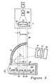
- Fig. 3 is an illustration of an etch rate monitor in accordance with the present invention in which reflective optical system, such as concave spherical mirror 44, is used in lieu of collection optics 36 , shown in Fig. 1, to converge the diffracted light from semiconductor wafer 12 onto collimating lens 42, interference filters 40 and detector 38.
- Concave mirror 44 is provided with an opening, not shown, which permits unobstructed passage of incident collimated light beam 30 from light source optics 32 through window 26 to semiconductor wafer 12.
- Spherical concave mirror 44 provides the same quality of light collection as a positive lens used as collection optics 36 as shown in Fig. 1 and substantially superior quality of light collection than a Fresnel lens would under the same circumstances.
- concave mirror 44 does not have the attenuation and losses associated with a very thick positive lens, nor the weight. Because concave mirror 44 permits the diffraction orders to be redirected by reflection to collimating lens 42, interference filters 40 and detector 38, these devices may be mounted closer to etch chamber 10 making the resultant device more compact and enclosable.
- Fig. 4 is an illustration of still another embodiment of an etch rate monitor in accordance with the present invention in which photodetector 46 is used in lieu of collection optics 36, shown in Fig. 1, or concave mirror 44, shown in Fig. 3, to collect and detect the diffracted light from semiconductor wafer 12.
- Interference filters 40 may conveniently be positioned between photodetector 46 and window 26.
- Heat transfer requirements for photodetector 46 and/or etch chamber 10 may be conveniently handled by positioning heat exchanger 48 on the surface of photodetector 46 opposite interference filters 40.
- Heat exchanger 48 may be a liquid cooled heat exchanger ensuring consistent performance of photodetector 46 and be provided with coolant in flow port 50 and out flow port 52.
- Photodetector 46, and heat exchanger 48 must be provided with an opening, not shown, which permits unobstructed passage of incident collimated light beam 30 from light source optics 32 through window 26 to semiconductor wafer 12.
- Interference filters 40 permit passage of light with the wavelengths in incident collimated light beam 30 and reject light with wavelengths different therefrom so that an opening within interference filters 40 for passage of incident collimated light beam 30 is not required.
- Photodetector 46 may be a single photodetector or an array of such photodetectors, depending upon the application.
- the advantages of photodetector 46 over concave mirror 44 shown in Fig. 2 or collection optics 36 shown in Fig. 1 are simplicity, compactness and convenience.
Landscapes
- Physics & Mathematics (AREA)
- General Physics & Mathematics (AREA)
- Drying Of Semiconductors (AREA)
- Testing Or Measuring Of Semiconductors Or The Like (AREA)
Applications Claiming Priority (2)
| Application Number | Priority Date | Filing Date | Title |
|---|---|---|---|
| US54066090A | 1990-06-19 | 1990-06-19 | |
| US540660 | 1990-06-19 |
Publications (3)
| Publication Number | Publication Date |
|---|---|
| EP0462599A2 true EP0462599A2 (de) | 1991-12-27 |
| EP0462599A3 EP0462599A3 (en) | 1992-08-12 |
| EP0462599B1 EP0462599B1 (de) | 1996-02-14 |
Family
ID=24156415
Family Applications (1)
| Application Number | Title | Priority Date | Filing Date |
|---|---|---|---|
| EP91110089A Expired - Lifetime EP0462599B1 (de) | 1990-06-19 | 1991-06-19 | Vorrichtung und Verfahren zum Messen der Ätzgeschwindigkeit |
Country Status (4)
| Country | Link |
|---|---|
| EP (1) | EP0462599B1 (de) |
| JP (1) | JP3065380B2 (de) |
| KR (1) | KR100226002B1 (de) |
| DE (1) | DE69117103T2 (de) |
Cited By (4)
| Publication number | Priority date | Publication date | Assignee | Title |
|---|---|---|---|---|
| WO2002077715A3 (en) * | 2001-03-21 | 2003-05-22 | Intel Corp | Method of fabrication to sharpen corners of waveguide y-branches in integrated optical components |
| WO2005020294A3 (en) * | 2003-08-20 | 2005-06-02 | Boc Group Inc | “control of etch and deposition processes” |
| ES2540921A1 (es) * | 2015-03-06 | 2015-07-14 | Universidad Complutense De Madrid | Dispositivo opto-electrónico y métodos para colimar y determinar el grado de colimación de un haz de luz |
| WO2024091628A1 (en) * | 2022-10-28 | 2024-05-02 | Applied Materials, Inc. | Methods of geometry parameters measurement for optical gratings |
Families Citing this family (2)
| Publication number | Priority date | Publication date | Assignee | Title |
|---|---|---|---|---|
| US6687015B1 (en) | 1999-06-28 | 2004-02-03 | Fraunhofer Gesellschaft Zur Forderung Der Angewandten Forschung E.V. | Method and device for measuring the thickness of a layer |
| JP5920255B2 (ja) * | 2013-03-18 | 2016-05-18 | 株式会社デンソー | 半導体装置の製造方法およびそれに用いられるドライエッチング装置 |
Family Cites Families (3)
| Publication number | Priority date | Publication date | Assignee | Title |
|---|---|---|---|---|
| US4927485A (en) * | 1988-07-28 | 1990-05-22 | Applied Materials, Inc. | Laser interferometer system for monitoring and controlling IC processing |
| US4873430A (en) * | 1988-10-25 | 1989-10-10 | International Business Machines Corporation | Method and apparatus for optically measuring characteristics of a thin film by directing a P-polarized beam through an integrating sphere at the brewster's angle of the film |
| JPH088242B2 (ja) * | 1989-10-31 | 1996-01-29 | 株式会社東芝 | エッチング深さ測定装置 |
-
1991
- 1991-06-19 DE DE69117103T patent/DE69117103T2/de not_active Expired - Fee Related
- 1991-06-19 JP JP3147323A patent/JP3065380B2/ja not_active Expired - Fee Related
- 1991-06-19 EP EP91110089A patent/EP0462599B1/de not_active Expired - Lifetime
- 1991-06-19 KR KR1019910010173A patent/KR100226002B1/ko not_active Expired - Fee Related
Cited By (7)
| Publication number | Priority date | Publication date | Assignee | Title |
|---|---|---|---|---|
| WO2002077715A3 (en) * | 2001-03-21 | 2003-05-22 | Intel Corp | Method of fabrication to sharpen corners of waveguide y-branches in integrated optical components |
| US6730988B2 (en) | 2001-03-21 | 2004-05-04 | Intel Corporation | Method of fabrication to sharpen corners of Y-branches in integrated optical components and other micro-devices |
| US6818559B2 (en) | 2001-03-21 | 2004-11-16 | Intel Corporation | Method of fabrication to sharpen corners of Y-branches in integrated optical components and other micro-devices |
| WO2005020294A3 (en) * | 2003-08-20 | 2005-06-02 | Boc Group Inc | “control of etch and deposition processes” |
| ES2540921A1 (es) * | 2015-03-06 | 2015-07-14 | Universidad Complutense De Madrid | Dispositivo opto-electrónico y métodos para colimar y determinar el grado de colimación de un haz de luz |
| WO2016142558A1 (es) * | 2015-03-06 | 2016-09-15 | Universidad Complutense De Madrid | Dispositivo opto-electrónico y método para colimar y determinar el grado de colimación de un haz de luz |
| WO2024091628A1 (en) * | 2022-10-28 | 2024-05-02 | Applied Materials, Inc. | Methods of geometry parameters measurement for optical gratings |
Also Published As
| Publication number | Publication date |
|---|---|
| JP3065380B2 (ja) | 2000-07-17 |
| JPH04297028A (ja) | 1992-10-21 |
| EP0462599A3 (en) | 1992-08-12 |
| KR100226002B1 (ko) | 1999-10-15 |
| EP0462599B1 (de) | 1996-02-14 |
| KR920001667A (ko) | 1992-01-30 |
| DE69117103D1 (de) | 1996-03-28 |
| DE69117103T2 (de) | 1996-06-27 |
Similar Documents
| Publication | Publication Date | Title |
|---|---|---|
| US5337144A (en) | Etch rate monitor using collimated light and method of using same | |
| EP0352740B1 (de) | Laserinterferometersystem zum Überwachen und Regeln der Bearbeitung von integrierten Schaltungen | |
| US7134933B2 (en) | Wafer thickness control during backside grind | |
| EP0566217B1 (de) | Verfahren und Gerät zum Fokussieren eines Strahls elektromagnetischer Energie | |
| US6100991A (en) | Near normal incidence optical assaying method and system having wavelength and angle sensitivity | |
| EP0718595B1 (de) | Automatische Unterdrückung von Diffraktionseffekten in Dünnfilmmessungen | |
| EP0168988B1 (de) | Durch einen eine Kristallstruktur aufweisenden Kolloid gebildeter Schmalbandstrahlungsfilter | |
| US4823169A (en) | Reflection density measuring system | |
| EP0899548B1 (de) | Kreuzkorrelationsverfahren und Vorrichtung zur Unterdrückung der Effekte von Mehrfachstreuung | |
| US20080202209A1 (en) | Sensor | |
| EP0632256B1 (de) | Mikropolarimeter, Mikrosensorsystem und Methode zum charakterisieren Dünner Filme | |
| JPH04303745A (ja) | 干渉光放射検出方法及びそのための装置 | |
| US6184985B1 (en) | Spectrometer configured to provide simultaneous multiple intensity spectra from independent light sources | |
| US4815856A (en) | Method and apparatus for measuring the absolute thickness of dust defocus layers | |
| EP0462599A2 (de) | Vorrichtung und Verfahren zum Messen der Ätzgeschwindigkeit | |
| WO2005020294A2 (en) | “control of etch and deposition processes” | |
| US5199058A (en) | X-ray monochromator and spectral measurement apparatus using the x-ray monochromator | |
| US4835381A (en) | Wide field of view radiant energy receiver | |
| JP2000506274A (ja) | ホログラフィーガス分析器 | |
| EP0059836B1 (de) | Optischer Strahlenteiler | |
| GB2075706A (en) | Grazing incidence spectrometer | |
| US5521995A (en) | Segmented waveguide gratings used as optical tilt and displacement sensors | |
| JP3338118B2 (ja) | 半導体装置の製造方法 | |
| EP0844465B1 (de) | Verfahren und Vorrichtung zum Überwachen einer ausgedehnten Strahlungsquelle mit Einzelelement-Detetektor-Messung mittels räumlicher Filterung und unter Ausnutzung der chromatischen Aberration der Abbildungsoptik | |
| WO1996024034A1 (en) | Method for improving optical measurement of rough samples in ellipsometry and reflectometry |
Legal Events
| Date | Code | Title | Description |
|---|---|---|---|
| PUAI | Public reference made under article 153(3) epc to a published international application that has entered the european phase |
Free format text: ORIGINAL CODE: 0009012 |
|
| AK | Designated contracting states |
Kind code of ref document: A2 Designated state(s): DE FR GB IT NL |
|
| PUAL | Search report despatched |
Free format text: ORIGINAL CODE: 0009013 |
|
| AK | Designated contracting states |
Kind code of ref document: A3 Designated state(s): DE FR GB IT NL |
|
| 17P | Request for examination filed |
Effective date: 19921204 |
|
| 17Q | First examination report despatched |
Effective date: 19940118 |
|
| ITF | It: translation for a ep patent filed | ||
| GRAA | (expected) grant |
Free format text: ORIGINAL CODE: 0009210 |
|
| AK | Designated contracting states |
Kind code of ref document: B1 Designated state(s): DE FR GB IT NL |
|
| REF | Corresponds to: |
Ref document number: 69117103 Country of ref document: DE Date of ref document: 19960328 |
|
| ET | Fr: translation filed | ||
| PLBE | No opposition filed within time limit |
Free format text: ORIGINAL CODE: 0009261 |
|
| STAA | Information on the status of an ep patent application or granted ep patent |
Free format text: STATUS: NO OPPOSITION FILED WITHIN TIME LIMIT |
|
| 26N | No opposition filed | ||
| PGFP | Annual fee paid to national office [announced via postgrant information from national office to epo] |
Ref country code: GB Payment date: 19970610 Year of fee payment: 7 |
|
| PGFP | Annual fee paid to national office [announced via postgrant information from national office to epo] |
Ref country code: FR Payment date: 19970620 Year of fee payment: 7 |
|
| PGFP | Annual fee paid to national office [announced via postgrant information from national office to epo] |
Ref country code: DE Payment date: 19970627 Year of fee payment: 7 |
|
| PGFP | Annual fee paid to national office [announced via postgrant information from national office to epo] |
Ref country code: NL Payment date: 19970630 Year of fee payment: 7 |
|
| PG25 | Lapsed in a contracting state [announced via postgrant information from national office to epo] |
Ref country code: GB Free format text: LAPSE BECAUSE OF NON-PAYMENT OF DUE FEES Effective date: 19980619 |
|
| PG25 | Lapsed in a contracting state [announced via postgrant information from national office to epo] |
Ref country code: NL Free format text: LAPSE BECAUSE OF NON-PAYMENT OF DUE FEES Effective date: 19990101 |
|
| GBPC | Gb: european patent ceased through non-payment of renewal fee |
Effective date: 19980619 |
|
| PG25 | Lapsed in a contracting state [announced via postgrant information from national office to epo] |
Ref country code: FR Free format text: LAPSE BECAUSE OF NON-PAYMENT OF DUE FEES Effective date: 19990226 |
|
| NLV4 | Nl: lapsed or anulled due to non-payment of the annual fee |
Effective date: 19990101 |
|
| PG25 | Lapsed in a contracting state [announced via postgrant information from national office to epo] |
Ref country code: DE Free format text: LAPSE BECAUSE OF NON-PAYMENT OF DUE FEES Effective date: 19990401 |
|
| REG | Reference to a national code |
Ref country code: FR Ref legal event code: ST |
|
| PG25 | Lapsed in a contracting state [announced via postgrant information from national office to epo] |
Ref country code: IT Free format text: LAPSE BECAUSE OF NON-PAYMENT OF DUE FEES;WARNING: LAPSES OF ITALIAN PATENTS WITH EFFECTIVE DATE BEFORE 2007 MAY HAVE OCCURRED AT ANY TIME BEFORE 2007. THE CORRECT EFFECTIVE DATE MAY BE DIFFERENT FROM THE ONE RECORDED. Effective date: 20050619 |