EP0461648B1 - Metal-insulator-metal type matrix liquid cristal display free from image sticking - Google Patents
Metal-insulator-metal type matrix liquid cristal display free from image sticking Download PDFInfo
- Publication number
- EP0461648B1 EP0461648B1 EP91109700A EP91109700A EP0461648B1 EP 0461648 B1 EP0461648 B1 EP 0461648B1 EP 91109700 A EP91109700 A EP 91109700A EP 91109700 A EP91109700 A EP 91109700A EP 0461648 B1 EP0461648 B1 EP 0461648B1
- Authority
- EP
- European Patent Office
- Prior art keywords
- mim
- metal
- electrode
- lcd
- characteristic
- Prior art date
- Legal status (The legal status is an assumption and is not a legal conclusion. Google has not performed a legal analysis and makes no representation as to the accuracy of the status listed.)
- Expired - Lifetime
Links
- 229910052751 metal Inorganic materials 0.000 title claims description 9
- 239000002184 metal Substances 0.000 title claims description 9
- 239000011159 matrix material Substances 0.000 title description 4
- PEDCQBHIVMGVHV-UHFFFAOYSA-N Glycerine Chemical compound OCC(O)CO PEDCQBHIVMGVHV-UHFFFAOYSA-N 0.000 title 2
- 239000007788 liquid Substances 0.000 title 1
- 239000004973 liquid crystal related substance Substances 0.000 claims description 33
- 239000000758 substrate Substances 0.000 claims description 29
- 239000011521 glass Substances 0.000 description 27
- 239000010410 layer Substances 0.000 description 21
- 238000000034 method Methods 0.000 description 21
- 238000000206 photolithography Methods 0.000 description 19
- 238000000059 patterning Methods 0.000 description 15
- XOLBLPGZBRYERU-UHFFFAOYSA-N tin dioxide Chemical compound O=[Sn]=O XOLBLPGZBRYERU-UHFFFAOYSA-N 0.000 description 14
- 229910052581 Si3N4 Inorganic materials 0.000 description 11
- HQVNEWCFYHHQES-UHFFFAOYSA-N silicon nitride Chemical compound N12[Si]34N5[Si]62N3[Si]51N64 HQVNEWCFYHHQES-UHFFFAOYSA-N 0.000 description 11
- VYPSYNLAJGMNEJ-UHFFFAOYSA-N Silicium dioxide Chemical compound O=[Si]=O VYPSYNLAJGMNEJ-UHFFFAOYSA-N 0.000 description 10
- 239000011241 protective layer Substances 0.000 description 10
- 238000010586 diagram Methods 0.000 description 7
- BLRPTPMANUNPDV-UHFFFAOYSA-N Silane Chemical compound [SiH4] BLRPTPMANUNPDV-UHFFFAOYSA-N 0.000 description 5
- 238000000354 decomposition reaction Methods 0.000 description 5
- 229920006332 epoxy adhesive Polymers 0.000 description 5
- 239000003365 glass fiber Substances 0.000 description 5
- 238000007789 sealing Methods 0.000 description 5
- 125000006850 spacer group Chemical group 0.000 description 5
- 229910052681 coesite Inorganic materials 0.000 description 4
- 229910052906 cristobalite Inorganic materials 0.000 description 4
- 239000000377 silicon dioxide Substances 0.000 description 4
- 229910052682 stishovite Inorganic materials 0.000 description 4
- 229910052905 tridymite Inorganic materials 0.000 description 4
- 239000000463 material Substances 0.000 description 2
- HBMJWWWQQXIZIP-UHFFFAOYSA-N silicon carbide Chemical compound [Si+]#[C-] HBMJWWWQQXIZIP-UHFFFAOYSA-N 0.000 description 2
- 229910010271 silicon carbide Inorganic materials 0.000 description 2
- 229910052814 silicon oxide Inorganic materials 0.000 description 2
- CMSGUKVDXXTJDQ-UHFFFAOYSA-N 4-(2-naphthalen-1-ylethylamino)-4-oxobutanoic acid Chemical compound C1=CC=C2C(CCNC(=O)CCC(=O)O)=CC=CC2=C1 CMSGUKVDXXTJDQ-UHFFFAOYSA-N 0.000 description 1
- 229910004205 SiNX Inorganic materials 0.000 description 1
- 230000000694 effects Effects 0.000 description 1
- 238000005516 engineering process Methods 0.000 description 1
- 238000001704 evaporation Methods 0.000 description 1
- AMGQUBHHOARCQH-UHFFFAOYSA-N indium;oxotin Chemical compound [In].[Sn]=O AMGQUBHHOARCQH-UHFFFAOYSA-N 0.000 description 1
- 238000001459 lithography Methods 0.000 description 1
- 238000004519 manufacturing process Methods 0.000 description 1
- 238000005457 optimization Methods 0.000 description 1
- 239000007787 solid Substances 0.000 description 1
Images


Classifications
-
- G—PHYSICS
- G09—EDUCATION; CRYPTOGRAPHY; DISPLAY; ADVERTISING; SEALS
- G09G—ARRANGEMENTS OR CIRCUITS FOR CONTROL OF INDICATING DEVICES USING STATIC MEANS TO PRESENT VARIABLE INFORMATION
- G09G3/00—Control arrangements or circuits, of interest only in connection with visual indicators other than cathode-ray tubes
- G09G3/20—Control arrangements or circuits, of interest only in connection with visual indicators other than cathode-ray tubes for presentation of an assembly of a number of characters, e.g. a page, by composing the assembly by combination of individual elements arranged in a matrix no fixed position being assigned to or needed to be assigned to the individual characters or partial characters
- G09G3/34—Control arrangements or circuits, of interest only in connection with visual indicators other than cathode-ray tubes for presentation of an assembly of a number of characters, e.g. a page, by composing the assembly by combination of individual elements arranged in a matrix no fixed position being assigned to or needed to be assigned to the individual characters or partial characters by control of light from an independent source
- G09G3/36—Control arrangements or circuits, of interest only in connection with visual indicators other than cathode-ray tubes for presentation of an assembly of a number of characters, e.g. a page, by composing the assembly by combination of individual elements arranged in a matrix no fixed position being assigned to or needed to be assigned to the individual characters or partial characters by control of light from an independent source using liquid crystals
- G09G3/3611—Control of matrices with row and column drivers
- G09G3/367—Control of matrices with row and column drivers with a nonlinear element in series with the liquid crystal cell, e.g. a diode, or M.I.M. element
-
- G—PHYSICS
- G02—OPTICS
- G02F—OPTICAL DEVICES OR ARRANGEMENTS FOR THE CONTROL OF LIGHT BY MODIFICATION OF THE OPTICAL PROPERTIES OF THE MEDIA OF THE ELEMENTS INVOLVED THEREIN; NON-LINEAR OPTICS; FREQUENCY-CHANGING OF LIGHT; OPTICAL LOGIC ELEMENTS; OPTICAL ANALOGUE/DIGITAL CONVERTERS
- G02F1/00—Devices or arrangements for the control of the intensity, colour, phase, polarisation or direction of light arriving from an independent light source, e.g. switching, gating or modulating; Non-linear optics
- G02F1/01—Devices or arrangements for the control of the intensity, colour, phase, polarisation or direction of light arriving from an independent light source, e.g. switching, gating or modulating; Non-linear optics for the control of the intensity, phase, polarisation or colour
- G02F1/13—Devices or arrangements for the control of the intensity, colour, phase, polarisation or direction of light arriving from an independent light source, e.g. switching, gating or modulating; Non-linear optics for the control of the intensity, phase, polarisation or colour based on liquid crystals, e.g. single liquid crystal display cells
- G02F1/133—Constructional arrangements; Operation of liquid crystal cells; Circuit arrangements
- G02F1/136—Liquid crystal cells structurally associated with a semi-conducting layer or substrate, e.g. cells forming part of an integrated circuit
- G02F1/1362—Active matrix addressed cells
- G02F1/1365—Active matrix addressed cells in which the switching element is a two-electrode device
-
- G—PHYSICS
- G02—OPTICS
- G02F—OPTICAL DEVICES OR ARRANGEMENTS FOR THE CONTROL OF LIGHT BY MODIFICATION OF THE OPTICAL PROPERTIES OF THE MEDIA OF THE ELEMENTS INVOLVED THEREIN; NON-LINEAR OPTICS; FREQUENCY-CHANGING OF LIGHT; OPTICAL LOGIC ELEMENTS; OPTICAL ANALOGUE/DIGITAL CONVERTERS
- G02F1/00—Devices or arrangements for the control of the intensity, colour, phase, polarisation or direction of light arriving from an independent light source, e.g. switching, gating or modulating; Non-linear optics
- G02F1/01—Devices or arrangements for the control of the intensity, colour, phase, polarisation or direction of light arriving from an independent light source, e.g. switching, gating or modulating; Non-linear optics for the control of the intensity, phase, polarisation or colour
- G02F1/13—Devices or arrangements for the control of the intensity, colour, phase, polarisation or direction of light arriving from an independent light source, e.g. switching, gating or modulating; Non-linear optics for the control of the intensity, phase, polarisation or colour based on liquid crystals, e.g. single liquid crystal display cells
- G02F1/133—Constructional arrangements; Operation of liquid crystal cells; Circuit arrangements
- G02F1/136—Liquid crystal cells structurally associated with a semi-conducting layer or substrate, e.g. cells forming part of an integrated circuit
- G02F1/1362—Active matrix addressed cells
- G02F1/13624—Active matrix addressed cells having more than one switching element per pixel
-
- G—PHYSICS
- G09—EDUCATION; CRYPTOGRAPHY; DISPLAY; ADVERTISING; SEALS
- G09G—ARRANGEMENTS OR CIRCUITS FOR CONTROL OF INDICATING DEVICES USING STATIC MEANS TO PRESENT VARIABLE INFORMATION
- G09G2300/00—Aspects of the constitution of display devices
- G09G2300/08—Active matrix structure, i.e. with use of active elements, inclusive of non-linear two terminal elements, in the pixels together with light emitting or modulating elements
- G09G2300/0809—Several active elements per pixel in active matrix panels
-
- G—PHYSICS
- G09—EDUCATION; CRYPTOGRAPHY; DISPLAY; ADVERTISING; SEALS
- G09G—ARRANGEMENTS OR CIRCUITS FOR CONTROL OF INDICATING DEVICES USING STATIC MEANS TO PRESENT VARIABLE INFORMATION
- G09G3/00—Control arrangements or circuits, of interest only in connection with visual indicators other than cathode-ray tubes
- G09G3/20—Control arrangements or circuits, of interest only in connection with visual indicators other than cathode-ray tubes for presentation of an assembly of a number of characters, e.g. a page, by composing the assembly by combination of individual elements arranged in a matrix no fixed position being assigned to or needed to be assigned to the individual characters or partial characters
- G09G3/2007—Display of intermediate tones
- G09G3/2014—Display of intermediate tones by modulation of the duration of a single pulse during which the logic level remains constant
Definitions
- the present invention relates liquid crystal display which employs a metal-insulator-metal (referred to as MIM hereinafter) element, as mentioned in the introductory portion of claim 1.
- MIM metal-insulator-metal
- LCDS liquid crystal displays
- MIMs metal-Insulator-Metal Nonlinear Devices for Use in Multiplexed Liquid Crystal Displays
- S. Morozumi, et al. "Lateral MIM-LCD with 250x240 Pixels,” Technical Reports of Television Society of Japan (IPD83-8), pp. 39-44, December, 1983.
- JP-A-1 076 038 discloses an MIM-element and a resistance element connected in series between a row electrode and a picture element electrode in an electrooptical device.
- the prior art JP-A-63 303 322 discloses the use of liquid crystal as the electrooptical medium in display devices comprising nonlinear resistance elements, picture electrodes, row electrodes and column electrodes.
- FIG. 1 An equivalent circuit per pixel of the prior art MIM-LCD is shown in Fig. 1.
- a liquid crystal element 5 and an MIM element 18 are connected in series between a lead electrode 9 and a transparent counter electrode 15.
- the MIM element 18 operates as a nonlinear resistor element.
- I-V current-voltage
- a constant resistor element 22 is connected between an MIM element 18 and a liquid crystal element 5.
- the I-V characteristic of the circuit in which the constant resistor element 22 and the MIM element 18 are connected in series is as shown in Fig. 4.
- the above-mentioned I-V characteristic is determined by the I-V characteristic of the MIM element 18 (region 30), while for the high values of the voltage V the I-V characteristic is determined by the I-V characteristic of the constant resistance element (region 31).
- the driving voltage Vd of the liquid crystal element 5 is chosen within the region 31, the voltage applied to the liquid crystal element 5 will not change even though the I-V characteristic of the MIM element 18 is changed, and the display characteristic of the liquid crystal will not change either.
- pixels 12 are arranged in a matrix form on a lower glass substrate 6.
- the pixels of each row are respectively connected to a lead electrode 9 for each row via MIM elements (not shown), and one end of the lead electrode 9 is connected to a terminal part 19.
- the terminal part 19 is connected to a driver circuit (not shown).
- a transparent counter electrode 15 Over the pixels of each column there is provided a transparent counter electrode 15 that is placed on an upper glass substrate 16.
- the lower glass substrate 6 is coated with a glass protective layer 21 of SiO 2 or the like. Since the protective layer 21 is not absolutely necessary it may be omitted if so desired.
- a Cr layer with thickness of 300 to 600 ⁇ is formed as a lower electrode, and an MIM element connecting electrode 17 which is to become the lower electrode of the MIM element is formed by the ordinary photolithography.
- a silicon nitride layer with thickness of 800 to 2000 ⁇ is formed as a nonlinear resistor 8 by a glow discharge decomposition method that uses SiH 4 gas and N 2 gas.
- a Cr layer with thickness of 1000 ⁇ is formed, and a lead electrode 9 and a constant resistor connecting electrode 7 are formed through patterning by the photolithography method.
- the silicon nitride layer is patterned by photolithography.
- a Ta layer with thickness of about 100 ⁇ is formed, and a constant resistor 10 is formed by patterning it in a slender meandering shape by photolithography. Then, an indium tin oxide (referred to as ITO hereinafter) film is formed as a pixel electrode 12 by patterning.
- ITO indium tin oxide
- an ITO film is formed on the upper glass substrate 16, and patterned it to form a transparent counter electrode 15.
- the lower glass substrate 6 and the upper glass substrate 16 are subjected to an orientation treatment, then laminated via a spacer such as glass fiber, and sealed with an ordinary epoxy adhesive, The thickness of the cell is set at 5 ⁇ m.
- a TN type liquid crystal is injected to form a liquid crystal layer 13.
- An MIM-LCD is completed by sealing the liquid crystal layer 13.
- nonlinear resistor 8 is constructed by using silicon nitride in the present embodiment, it may be constructed by using silicon carbide, silicon oxide, or the like.
- the nonlinear resistor 8 is formed on the MIM element connecting electrode 17, and on top of the nonlinear resistor 8 there are formed the lead electrode 9 and the constant resistor connecting electrode 7 on both ends of the connecting electrode 17 in the form to perpendicularly crossing the connecting electrode 17 so as to have equal crossing areas with the connecting electrode. Accordingly, by connecting a first MIM element consisting of the lead electrode 9, the nonlinear resistor 8 and the MIM element connecting electrode 17, and a second MIM element consisting of the constant resistor connecting element 7, the nonlinear resistor 8 and the MIM element connecting electrode 17, back-to-back in series between the lead electrode 9 and the constant resistor connecting electrode 7, it is possible to remove asymmetry based on the polarity change. Further, the constant resistor connecting electrode 7 is connected to the pixel electrode 12 through the constant resistor 10. As a result, there is obtained a structure that connects in series two MIM elements and the constant resistor 10 and the pixel electrode 12.
- an MIM-LCD is fabricated by switching the material for the constant resistor 10 from Ta to Sb-doped SnO 2 (usually referred to as an NESA film). Since the basic structure of the MIM-LCD obtained is the same as that shown in Figs. 5 to 7, its plan view alone is shown in Fig. 8.
- An Sb-doped SnO 2 film having resistivity of 5 x 10 -2 ⁇ cm is formed to a thickness of 100 ⁇ by an evaporation method, then a constant resistor 10 with resistance 1.1 x 10 7 ⁇ is formed by patterning the SnO 2 film so as to have a line width of 4 ⁇ m and a length of 883 ⁇ m.
- the nonlinear resistor 8 is formed of a silicon nitride film of thickness 1100 ⁇ .
- the I-V characteristic of the series connection of the MIM element 18 and the constant resistor 10 is as shown in Fig. 9. If the driving voltage Vd of the MIM-LCD is assumed to be 33 V, then it means that the I-V characteristic of the MIM-LCD is to use the region 31 which is dominated by the I-V characteristic of the constant resistor 10. Therefore, the voltage that is applied to the liquid crystal element is not changed and hence the display characteristic of the liquid crystal is not changed either even though there occurs a change in the I-V characteristic of the MIM element itself.
- the I-V characteristic in the range of the driving voltage of the MIM-LCD as a whole will not be changed even when the I-V characteristic of the MIM element changes. Consequently, the display characteristics of the liquid crystal is scarcely changed even though the I-V characteristic of the MIM element itself is changed.
- the I-V characteristic of a system obtained by connecting in series a first MIM element 1 having an I-V characteristic as shown in Fig. 10 and a first constant resistor 2 having an I-V characteristic as shown in Fig. 11 becomes as shown in Fig. 12.
- the I-V characteristic of a system obtained by connecting in series a second MIM element 3 having an I-V characteristic as shown in Fig. 13 and a second constant resistor 4 having an I-V characteristic as shown in Fig. 14 becomes as shown in Fig. 15.
- FIG. 17 An equivalent circuit for a nonlinear resistance element formed by connecting in parallel two sets of serially-connected MIM element and constant resistor is as shown in Fig. 17, and its I-V characteristic is as shown in Fig. 16.
- the regions of 0V-Va, Va-Vb, Vb-Vc and above Vc are determined by the I-V characteristics of the first MIM element 1, first constant resistor 2, second MIM element 3 and second constant resistor 4, respectively.
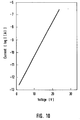
- the driving waveform is as shown in Fig. 18.
- the liquid crystal is turned on when the voltage is Ve, and is turned off when it is Vf.
- the gradation is controlled by changing the width of the pulse that is applied between the lead electrode 9 and the transparent counter electrode 15.
- the I-V characteristic in the vicinity of the driving voltage Ve and Vf will not change even if the I-V characteristics of the first MIM element 1 and the second MIM element 3 are changed. Accordingly, the changes in the I-V characteristic of the MIM elements does not appear as image stickings in the display of the pixel.
- Figs. 19 and 20 are a sectional view and a plan view on the surface of the lower substrate, respectively, of one pixel of the MIM-LCD obtained as a first application of the present embodiment.
- the lower glass substrate 6 is coated with a glass protective layer 21 made of SnO 2 or the like. Since this protective layer is not in dispensable, it may be omitted.
- a Cr film with thickness of 300 - 600 ⁇ or so is formed as a lower electrode, and a constant resistor connecting electrode 7 which become the lower electrodes of the MIM element and pixel connecting electrodes 11 are formed by the ordinary photolithography.
- an MIM element 8 of silicon nitride layer with thickness of 800 - 2000 ⁇ or so is formed by a glow discharge decomposition method that uses SiH 4 gas and N 2 gas, and a first MIM element 1 and a second MIM element 3 are formed by patterning the silicon nitride layer.
- a Cr film with thickness of 1000 ⁇ is formed as an upper electrode, and a lead electrode 9 is formed through patterning of the Cr film by a photolithography method.
- the area of the overlapped portion of the lower electrode and the upper electrode which represents the element area of the second MIM element 3 is so adjusted to be 1/40 to 1/20 of the element area of the first MIM element 1.
- a Ta film with a thickness of about 100 ⁇ which is to become the constant resistors 10 are formed, and a first constant resistor 2 and a second constant resistor 4 which has a width equal to, and a length 1/10 to 1/5 of, those of the first constant resistor 2, patterned in a slender and meandering shape are formed by a photolithography method.
- Pixel electrodes 12 are formed by patterning an ITO film.
- An ITO film is formed on an upper glass substrate 16, and a transparent counter electrode 15 is formed by patterning the film.
- the lower glass substrate 6 and the upper glass substrate 16 are subjected to an orientation treatment to form oriented films 14, laminated via a spacer such as glass fiber, then sealed with an ordinary epoxy adhesive.
- the thickness of the cell is set to be 5 ⁇ m.
- a TN type liquid crystal is injected to form a liquid crystal layer 13.
- An MIM-LCD is completed by sealing the liquid crystal layer. After a driving of the MIM-LCD for 10000 hours there was observed no image sticking.
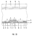
- Figs. 21 and 22 are a sectional view and a plan view on the lower substrate surface, respectively, of one pixel of the MIM-LCD obtained as a second application of the present embodiment.
- the lower glass substrate 6 is coated with a glass protective layer 21 made of SiO 2 .
- This protective layer 21 may be omitted since it is not absolutely necessary.
- a Cr film with thickness of 300 to 600 ⁇ or so is formed as a lower electrode, and MIM element connecting electrodes 17 which are to become the lower electrodes of the MIM element are formed by an ordinary photolithography method.
- an MIM element 8 made of a silicon nitride layer with thickness of 800 to 1500 ⁇ or so is formed by a glow discharge decomposition method that uses SiH 4 gas and N 2 gas, and a first MIM element 1 and a second MIM element 3 are patterned by an ordinary photolithography method.
- a Cr film with thickness of 1000 ⁇ is formed as an upper electrode, and a lead electrode 9 pixel connecting electrodes 11 and constant resistor connecting electrodes 7 are patterned by an ordinary photolithography method.
- the area of the overlapped portion of the lower electrode and the upper electrode which forms the element area of the second MIM element 3 is adjusted to be 1/40 to 1/20 of the element area of the first MIM element 1.
- a Ta film with thickness of about 100 ⁇ which becomes the constant resistors 10 is formed, and a constant resistor 2 and a second constant resistor 4, which has a width equal to, and a legnth 1/10 to 1/5 of, those of the first constant resistor 2, patterned in a slender and meandering shape are formed by a photolithography method.
- Pixel electrodes 12 are formed by patterning an ITO film.
- An ITO film is formed on an upper glass substrate 16, and a transparent counter electrode 15 is formed by patterning the film.
- the lower glass substrate 6 and the upper glass substrate 16 are subjected to an orientation treatment to form oriented films 14, laminated via a spacer such as glass fiber, then sealed with an ordinary epoxy adhesive.
- the thickness of the cell is set to be 5 ⁇ m.
- a TN type liquid crystal is injected to form a liquid crystal layer 13.
- An MIM-LCD is completed by sealing the liquid crystal layer. After a driving of the MIM-LCD for 10000 hours there was observed no image sticking.
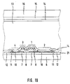
- Figs. 23 and 24 are a sectional view and a plan view on the lower substrate surface, respectively, of one pixel of the MIM-LCD obtained as a third application of the present embodiment.
- the lower glass substrate 6 is coated with a glass protective layer 21 made of SiO 2 .
- This protective layer 21 may be omitted since it is not absolutely necessary.
- a Cr film with thickness of 300 to 600 ⁇ or so is formed as a lower electrode, and constant resistor connecting electrodes 7 which is to become the lower electrodes of an MIM element and pixel connecting electrodes 11 are formed by an ordinary photolithography method.
- an MIM element 8 made of a silicon nitride layer with thickness of 800 to 2000 ⁇ or so is formed by an glow discharge decomposition method that uses SiH 4 gas and N 2 gas, and a first MIM element 1 and a second MIM element 3 are patterned by a photolithography method.
- a Cr film with thickness of 1000 ⁇ is formed as an upper electrode, and a lead electrode 9 is patterned by a photolithography method.
- the area of the overlapped portion of the lower electrode and the upper electrode which forms the element area of the second MIM element 3 is adjusted to be 1/40 to 1/20 of the element area of the first MIM element 1.
- an ITO film with thickness of about 300 ⁇ is formed, and a first constant resistor 2, a second constant resistor 4, which has a width equal to, and a length 1/10 to 1/5 of, those of the first constant resistor 2, and pixel electrodes 12 are formed by patterning the ITO film by the photolithography method.
- An ITO film is formed on an upper glass substrate 16, and a transparent counter electrode 15 is formed by patterning the film.
- the lower glass substrate 6 and the upper glass substrate 16 are subjected to an orientation treatment to form oriented films 14, laminated via a spacer such as glass fiber, then sealed with an ordinary epoxy adhesive.
- the thickness of the cell is set to be 5 ⁇ m.
- a TN type liquid crystal is injected fo form a liquid crystal layer 13.
- An MIM-LCD is completed by sealing the liquid crystal layer. After a driving of the MIM-LCD for 10000 hours there was observed no image sticking.
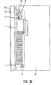
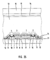
- Figs. 25 and 26 are a sectional view and a plan view on the lower substrate surface, respectively, of one pixel of the MIM-LCD obtained as a fourth application of the present embodiment.
- the lower glass substrate 6 is coated with a glass protective layer 21 made of SiO 2 . This protective layer 21 may be omitted since it is not absolutely necessary.
- a Cr film with thickness of 300 to 600 ⁇ or so is formed as a lower electrode, and MIM element connecting electrodes 17 that are to form the lower electrodes of an MIM element are formed by an ordinary photolithography method.
- an MIM element 8 made of silicon nitride layer with thickness of 800 to 1500 ⁇ or so is formed by the glow discharge decomposition method that uses SiH 4 gas and N 2 gas, and a first MIM element 1 and a second MIM element 3 are patterned by an ordinary photolithography method.
- a Cr film with a thickness of 1000 ⁇ is formed as an upper electrode, and a lead electrode 9, pixel connecting electrodes 11 and constant resistor connecting electrodes 7 are patterned by a photolithography method.
- the area of the overlapped portion of the lower electrode and the upper electrode which forms the element area of the second MIM element 3 is adjusted to be 1/40 to 1/20 of the element area of the first MIM element 1.
- an ITO film with a thcikness of about 300 ⁇ is formed, and a first constant resistor 2, a second constant resistor 4, which has a width equal to, and a length 1/10 to 1/5 of, those of the first constant resistor 2, and pixel electrodes 12 are formed by patterning the ITO film by 9 photolithography method.
- An ITO film is formed on an upper glass substrate 16 and a transparent counter electrode 15 is formed by patterning the film.
- the lower glass substrate 6 and the upper glass substrate 16 are subjected to an orientation treatment to form oriented films 14, laminated via a spacer such as glass fiber, then sealed with an ordinary epoxy adhesive,
- the thickness of the cell is set to be 5 ⁇ m.
- a TN type liquid crystal is injected to form a liquid crystal layer 13.
- An MIM-LCD is completed by sealing the liquid crystal layer. After a driving of the MIM-LCD for 10000 hours there was observed no image sticking.
- the MIM element 8 was constructed by using silicon nitride, but a similar effect can be obtained by constructing the element by using silicon carbide, silicon oxide, or the like.
- the I-V characteristic in the range of the voltages used for graduation display be pulse width modulation, will not change even if the I-V characteristic of the MIM elements is changed due to driving of the display over a long period of time. Therefore, there will occur no sticking of the display.
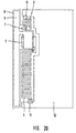
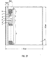
- an MIM-LCD as a fifth application of the present embodiment is manufactured by switching the material for the constant resistor 10 from Ta to Sb-doped SnO 2 .
- a plan view of the obtained device is shown in Fig. 27.
- a film with a thickness of 50 ⁇ of Sb-doped SnO 2 having resistivity of 5 x 10 -2 ⁇ cm is formed, then by patterning the film a first constant resistor with resistance 7.3 x 10 7 ⁇ and having line width of 2 ⁇ m and length of 1470 um, and a second constant resistor 4 with resistance 1.1 x 10 7 ⁇ and having line width of 2 ⁇ m and length of 220 ⁇ m, are formed.
- the I-V characteristic of the circuit consisting of a first and a second MIM elements 1 and 3, and a first and a second constant resistors 2 and 4 is as shown in Fig. 28.
Description
- The present invention relates liquid crystal display which employs a metal-insulator-metal (referred to as MIM hereinafter) element, as mentioned in the introductory portion of
claim 1. - As the past examples of liquid crystal displays (referred to as LCDS hereinafter) that employs MIMs, there may be mentioned those disclosed in D.R. Baraff, et al., "The Optimization of Metal-Insulator-Metal Nonlinear Devices for Use in Multiplexed Liquid Crystal Displays," IEEE Trans. Electron Devices, Vol. ED-28, pp. 736-739 (1981), and S. Morozumi, et al., "Lateral MIM-LCD with 250x240 Pixels," Technical Reports of Television Society of Japan (IPD83-8), pp. 39-44, December, 1983.
- In addition, an active matrix LCD which uses silicon nitride of small dielectric constant as a nonlinear resistor for MIM element is disclosed in M. Suzuki, et al. "A New Active Diode Matrix LCD Using Off-Stoichiometric SiNx Layers "Proceedings of the SID, Vol. 28, pp. 101-104 (1987).
- Further MIMs in an electrooptical device and LCDs are disclosed in the prior art JP-A 076 038 and JP-A-63-303 322.
- The prior art JP-A-1 076 038 discloses an MIM-element and a resistance element connected in series between a row electrode and a picture element electrode in an electrooptical device.
- The prior art JP-A-63 303 322 discloses the use of liquid crystal as the electrooptical medium in display devices comprising nonlinear resistance elements, picture electrodes, row electrodes and column electrodes.
- An equivalent circuit per pixel of the prior art MIM-LCD is shown in Fig. 1. A
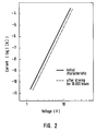
liquid crystal element 5 and anMIM element 18 are connected in series between alead electrode 9 and atransparent counter electrode 15. TheMIM element 18 operates as a nonlinear resistor element. When a voltage is applied for a long time between thelead electrode 9 and thetransparent counter electrode 15 in order to drive such an MIM-LCD over a long period of time, there occurs a change in the current-voltage (referred to as I-V hereinafter) characteristic as shown in Fig. 2. In Fig. 2, the solid and the broken lines represent the initial characteristic and the characteristic after drive for 10000 hours, respectively. With such a change in the I-V characteristic, even when a voltage which is the same as that before the change is applied between thelead electrode 9 and thetransparent counter electrode 15, the voltage applied to theliquid crystal 5 becomes different from that before the change, and its display characteristic is accordingly changed. This phenomenon is called image sticking. - It is, therefore, a major object of the present invention to provide an MIM-LCD which is free from image sticking.
- In accordance with the present invention, said object is obtained with the features of the characterizing portion of
claim 1. - The above and further objects, features and advantages of the present invention will become more apparent from the following detailed description taken in conjunction with the accompanying drawings, wherein:
- Fig. 1 is an equivalent circuit per pixel of the prior art MIM-LCD;
- Fig. 2 is a diagram for explaining an I-V characteristic of an MIM element;
- Fig. 3 is an equivalent circuit for explaining the MIM-LCD according to a first embodiment of the present invention;
- Fig. 4 is a diagram for I-V characteristic for explaining the MIM-LCD according to the first embodiment of the present invention;
- Fig. 5 is a plan view for explaining the first and a second embodiments of the present invention;
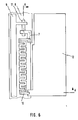
- Fig. 6 is a partial plan view for explaining the MIM-LCD of the first embodiment of the present invention;
- Fig. 7 is a sectional view taken along the AA line in Fig. 6;
- Fig. 8 is a plan view for explaining the MIM-LCD in which Sb-doped SnO2 is used as the constant resistor, presented as an application of the first embodiment of the present invention;
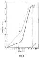
- Fig. 9 is the diagram for I-V characteristic of the MIM-LCD shown in Fig. 8;
- Figs. 10 to 16 are I-V characteristic diagrams for explaining the second embodiment of the present invention;
- Fig. 17 is an equivalent circuit diagram for explaining the MIM-LCD of the second embodiment of the present invention;
- Fig. 18 is a waveform diagram for driving the MIM-LCD of the second embodiment of the present invention;
- Fig. 19 is a sectional view of the MIM-LCD obtained as a first application of the second embodiment of the present invention;
- Fig. 20 is a plan view of the MIM-LCD obtained as the first application of the second embodiment of the present invention;
- Fig. 21 is a sectional view of the MIM-LCD obtained as a second application of the second embodiment of the present invention;
- Fig. 22 is a plan view of the MIM-LCD obtained as the second application of the second embodiment of the present invention;
- Fig. 23 is a sectional view of the MIM-LCD obtained as a third application of the second embodiment of the present invention;
- Fig. 24 is a plan view of the MIM-LCD obtained as the third application of the second embodiment of the present invention;
- Fig. 25 is a sectional view of the MIM-LCD obtained as a fourth application of the second embodiment of the present invention;
- Fig. 26 is a plan view of the MIM-LCD obtained as the fourth application of the second embodiment of the present invention;
- Fig. 27 is a plan view of the MIM-LCD obtained as a fifth application of the second embodiment of the present invention; and
- Fig. 28 is a diagram for I-V characteristic of the MIM-LCD shown in Fig. 27
- Referrint to Fig. 3, a
constant resistor element 22 is connected between anMIM element 18 and aliquid crystal element 5. The I-V characteristic of the circuit in which theconstant resistor element 22 and theMIM element 18 are connected in series is as shown in Fig. 4. For the low values of the voltage V the above-mentioned I-V characteristic is determined by the I-V characteristic of the MIM element 18 (region 30), while for the high values of the voltage V the I-V characteristic is determined by the I-V characteristic of the constant resistance element (region 31). When the driving voltage Vd of theliquid crystal element 5 is chosen within theregion 31, the voltage applied to theliquid crystal element 5 will not change even though the I-V characteristic of theMIM element 18 is changed, and the display characteristic of the liquid crystal will not change either. - Further, the driving voltage that is applied to the
liquid crystal element 5 is determined not by the I-V characteristic of theMIM element 18 but by the I-V characteristic of theconstant resistor element 22, so that the nonuniformity of display within the panel can also be improved. This is due to the following reasons. The variation in the I-V characteristic of theMIM element 18 is generated due mainly to the fluctuation in its film thickness. Since it is difficult to restrain the variation of the film thickness within the panel to within a certain predetermined range, it is accordingly difficult to improve the uniformity or display within the panel. On the other hand, the variation in the I-V characteristic of theconstant resistor element 22 is mainly due to the fluctuation in the accuracy of the length and width, namely, the accuracy of the planar processing of theelement 22. According to the presently available lithography technology it is relatively easy to confine the fluctuation in the planar dimensions within the panel to below predetermined values. Accordingly, it is possible to improve the nonuniformity of display within the panel by controlling the variation of theconstant resistor element 22 within the panel. - Next, referring to Figs. 5 to 7, the structure and the method of fabrication of the MIM-LCD according to the first embodiment of the present invention is described.
- Referring to Fig. 5,
pixels 12 are arranged in a matrix form on alower glass substrate 6. The pixels of each row are respectively connected to alead electrode 9 for each row via MIM elements (not shown), and one end of thelead electrode 9 is connected to aterminal part 19. Theterminal part 19 is connected to a driver circuit (not shown). Over the pixels of each column there is provided atransparent counter electrode 15 that is placed on anupper glass substrate 16. - Referring to Figs. 6 and 7, the
lower glass substrate 6 is coated with a glassprotective layer 21 of SiO2 or the like. Since theprotective layer 21 is not absolutely necessary it may be omitted if so desired. Next, a Cr layer with thickness of 300 to 600 Å is formed as a lower electrode, and an MIMelement connecting electrode 17 which is to become the lower electrode of the MIM element is formed by the ordinary photolithography. - Next, a silicon nitride layer with thickness of 800 to 2000 Å is formed as a
nonlinear resistor 8 by a glow discharge decomposition method that uses SiH4 gas and N2 gas. Following that, a Cr layer with thickness of 1000 Å is formed, and alead electrode 9 and a constantresistor connecting electrode 7 are formed through patterning by the photolithography method. Then, the silicon nitride layer is patterned by photolithography. - Next, a Ta layer with thickness of about 100 Å is formed, and a
constant resistor 10 is formed by patterning it in a slender meandering shape by photolithography. Then, an indium tin oxide (referred to as ITO hereinafter) film is formed as apixel electrode 12 by patterning. - Further, an ITO film is formed on the
upper glass substrate 16, and patterned it to form atransparent counter electrode 15. Thelower glass substrate 6 and theupper glass substrate 16 are subjected to an orientation treatment, then laminated via a spacer such as glass fiber, and sealed with an ordinary epoxy adhesive, The thickness of the cell is set at 5 µm. - Then, a TN type liquid crystal is injected to form a
liquid crystal layer 13. An MIM-LCD is completed by sealing theliquid crystal layer 13. - Although the
nonlinear resistor 8 is constructed by using silicon nitride in the present embodiment, it may be constructed by using silicon carbide, silicon oxide, or the like. - In an MIM element fabricated as in the above, the
nonlinear resistor 8 is formed on the MIMelement connecting electrode 17, and on top of thenonlinear resistor 8 there are formed thelead electrode 9 and the constantresistor connecting electrode 7 on both ends of the connectingelectrode 17 in the form to perpendicularly crossing the connectingelectrode 17 so as to have equal crossing areas with the connecting electrode. Accordingly, by connecting a first MIM element consisting of thelead electrode 9, thenonlinear resistor 8 and the MIMelement connecting electrode 17, and a second MIM element consisting of the constantresistor connecting element 7, thenonlinear resistor 8 and the MIMelement connecting electrode 17, back-to-back in series between thelead electrode 9 and the constantresistor connecting electrode 7, it is possible to remove asymmetry based on the polarity change. Further, the constantresistor connecting electrode 7 is connected to thepixel electrode 12 through theconstant resistor 10. As a result, there is obtained a structure that connects in series two MIM elements and theconstant resistor 10 and thepixel electrode 12. - Next, an MIM-LCD is fabricated by switching the material for the
constant resistor 10 from Ta to Sb-doped SnO2 (usually referred to as an NESA film). Since the basic structure of the MIM-LCD obtained is the same as that shown in Figs. 5 to 7, its plan view alone is shown in Fig. 8. An Sb-doped SnO2 film having resistivity of 5 x 10⁻² Ω·cm is formed to a thickness of 100 Å by an evaporation method, then aconstant resistor 10 with resistance 1.1 x 10⁷ Ω is formed by patterning the SnO2 film so as to have a line width of 4 µm and a length of 883 µm. Thenonlinear resistor 8 is formed of a silicon nitride film of thickness 1100 Å. The I-V characteristic of the series connection of theMIM element 18 and theconstant resistor 10 is as shown in Fig. 9. If the driving voltage Vd of the MIM-LCD is assumed to be 33 V, then it means that the I-V characteristic of the MIM-LCD is to use theregion 31 which is dominated by the I-V characteristic of theconstant resistor 10. Therefore, the voltage that is applied to the liquid crystal element is not changed and hence the display characteristic of the liquid crystal is not changed either even though there occurs a change in the I-V characteristic of the MIM element itself. - Namely, if the present embodiment is applied, the I-V characteristic in the range of the driving voltage of the MIM-LCD as a whole will not be changed even when the I-V characteristic of the MIM element changes. Consequently, the display characteristics of the liquid crystal is scarcely changed even though the I-V characteristic of the MIM element itself is changed.
- The MIM-LCD in accordance with the present embodiment will be described based on Figs. 10 to 16 that show the I-V characteristics of the various MIM elements and constant resistors and Fig. 17 that shows an equivalent circuit for one pixel.
- When two resistors are connected in series, the resistance of the resultant system becomes equal to the resistance of the higher of the two resistors, whereas when they are connected in parallel, the resistance of the resultant system becomes equal to the resistance of the lower of the two resistors. The I-V characteristic of a system obtained by connecting in series a
first MIM element 1 having an I-V characteristic as shown in Fig. 10 and a firstconstant resistor 2 having an I-V characteristic as shown in Fig. 11 becomes as shown in Fig. 12. The I-V characteristic of a system obtained by connecting in series asecond MIM element 3 having an I-V characteristic as shown in Fig. 13 and a secondconstant resistor 4 having an I-V characteristic as shown in Fig. 14 becomes as shown in Fig. 15. An equivalent circuit for a nonlinear resistance element formed by connecting in parallel two sets of serially-connected MIM element and constant resistor is as shown in Fig. 17, and its I-V characteristic is as shown in Fig. 16. In this I-V chart, the regions of 0V-Va, Va-Vb, Vb-Vc and above Vc are determined by the I-V characteristics of thefirst MIM element 1, firstconstant resistor 2,second MIM element 3 and secondconstant resistor 4, respectively. When the gradation display is performed by pulse width modulation, the driving waveform is as shown in Fig. 18. The liquid crystal is turned on when the voltage is Ve, and is turned off when it is Vf. The gradation is controlled by changing the width of the pulse that is applied between thelead electrode 9 and thetransparent counter electrode 15. When the resistances of the MIM elements and the constant resistors are so determined as to have the voltages of Ve and Vf of the driving waveform fall above Vc and within the range of Va to Vb, respectively, the I-V characteristic in the vicinity of the driving voltage Ve and Vf will not change even if the I-V characteristics of thefirst MIM element 1 and thesecond MIM element 3 are changed. Accordingly, the changes in the I-V characteristic of the MIM elements does not appear as image stickings in the display of the pixel. - Figs. 19 and 20 are a sectional view and a plan view on the surface of the lower substrate, respectively, of one pixel of the MIM-LCD obtained as a first application of the present embodiment. The
lower glass substrate 6 is coated with a glassprotective layer 21 made of SnO2 or the like. Since this protective layer is not in dispensable, it may be omitted. Next, a Cr film with thickness of 300 - 600 Å or so is formed as a lower electrode, and a constantresistor connecting electrode 7 which become the lower electrodes of the MIM element andpixel connecting electrodes 11 are formed by the ordinary photolithography. Then, anMIM element 8 of silicon nitride layer with thickness of 800 - 2000 Å or so is formed by a glow discharge decomposition method that uses SiH4 gas and N2 gas, and afirst MIM element 1 and asecond MIM element 3 are formed by patterning the silicon nitride layer. Following that, a Cr film with thickness of 1000 Å is formed as an upper electrode, and alead electrode 9 is formed through patterning of the Cr film by a photolithography method. In this process the area of the overlapped portion of the lower electrode and the upper electrode which represents the element area of thesecond MIM element 3 is so adjusted to be 1/40 to 1/20 of the element area of thefirst MIM element 1. Further, a Ta film with a thickness of about 100 Å which is to become theconstant resistors 10 are formed, and a firstconstant resistor 2 and a secondconstant resistor 4 which has a width equal to, and alength 1/10 to 1/5 of, those of the firstconstant resistor 2, patterned in a slender and meandering shape are formed by a photolithography method.Pixel electrodes 12 are formed by patterning an ITO film. - An ITO film is formed on an
upper glass substrate 16, and atransparent counter electrode 15 is formed by patterning the film. Thelower glass substrate 6 and theupper glass substrate 16 are subjected to an orientation treatment to form orientedfilms 14, laminated via a spacer such as glass fiber, then sealed with an ordinary epoxy adhesive. The thickness of the cell is set to be 5 µm. - Then, a TN type liquid crystal is injected to form a
liquid crystal layer 13. An MIM-LCD is completed by sealing the liquid crystal layer. After a driving of the MIM-LCD for 10000 hours there was observed no image sticking. - Figs. 21 and 22 are a sectional view and a plan view on the lower substrate surface, respectively, of one pixel of the MIM-LCD obtained as a second application of the present embodiment. The
lower glass substrate 6 is coated with a glassprotective layer 21 made of SiO2. Thisprotective layer 21 may be omitted since it is not absolutely necessary. Next, a Cr film with thickness of 300 to 600 Å or so is formed as a lower electrode, and MIMelement connecting electrodes 17 which are to become the lower electrodes of the MIM element are formed by an ordinary photolithography method. Next, anMIM element 8 made of a silicon nitride layer with thickness of 800 to 1500 Å or so is formed by a glow discharge decomposition method that uses SiH4 gas and N2 gas, and afirst MIM element 1 and asecond MIM element 3 are patterned by an ordinary photolithography method. Following that, a Cr film with thickness of 1000 Å is formed as an upper electrode, and alead electrode 9pixel connecting electrodes 11 and constantresistor connecting electrodes 7 are patterned by an ordinary photolithography method. At this time, the area of the overlapped portion of the lower electrode and the upper electrode which forms the element area of thesecond MIM element 3 is adjusted to be 1/40 to 1/20 of the element area of thefirst MIM element 1. Further, a Ta film with thickness of about 100 Å which becomes theconstant resistors 10 is formed, and aconstant resistor 2 and a secondconstant resistor 4, which has a width equal to, and alegnth 1/10 to 1/5 of, those of the firstconstant resistor 2, patterned in a slender and meandering shape are formed by a photolithography method.Pixel electrodes 12 are formed by patterning an ITO film. - An ITO film is formed on an
upper glass substrate 16, and atransparent counter electrode 15 is formed by patterning the film. Thelower glass substrate 6 and theupper glass substrate 16 are subjected to an orientation treatment to form orientedfilms 14, laminated via a spacer such as glass fiber, then sealed with an ordinary epoxy adhesive. The thickness of the cell is set to be 5 µm. - Then, a TN type liquid crystal is injected to form a
liquid crystal layer 13. An MIM-LCD is completed by sealing the liquid crystal layer. After a driving of the MIM-LCD for 10000 hours there was observed no image sticking. - Figs. 23 and 24 are a sectional view and a plan view on the lower substrate surface, respectively, of one pixel of the MIM-LCD obtained as a third application of the present embodiment. The
lower glass substrate 6 is coated with a glassprotective layer 21 made of SiO2. Thisprotective layer 21 may be omitted since it is not absolutely necessary. Next, a Cr film with thickness of 300 to 600 Å or so is formed as a lower electrode, and constantresistor connecting electrodes 7 which is to become the lower electrodes of an MIM element andpixel connecting electrodes 11 are formed by an ordinary photolithography method. Next, anMIM element 8 made of a silicon nitride layer with thickness of 800 to 2000 Å or so is formed by an glow discharge decomposition method that uses SiH4 gas and N2 gas, and afirst MIM element 1 and asecond MIM element 3 are patterned by a photolithography method. Following that, a Cr film with thickness of 1000 Å is formed as an upper electrode, and alead electrode 9 is patterned by a photolithography method. At this time, the area of the overlapped portion of the lower electrode and the upper electrode which forms the element area of thesecond MIM element 3 is adjusted to be 1/40 to 1/20 of the element area of thefirst MIM element 1. Further, an ITO film with thickness of about 300 Å is formed, and a firstconstant resistor 2, a secondconstant resistor 4, which has a width equal to, and alength 1/10 to 1/5 of, those of the firstconstant resistor 2, andpixel electrodes 12 are formed by patterning the ITO film by the photolithography method. - An ITO film is formed on an
upper glass substrate 16, and atransparent counter electrode 15 is formed by patterning the film. Thelower glass substrate 6 and theupper glass substrate 16 are subjected to an orientation treatment to form orientedfilms 14, laminated via a spacer such as glass fiber, then sealed with an ordinary epoxy adhesive. The thickness of the cell is set to be 5 µm. - Then, a TN type liquid crystal is injected fo form a
liquid crystal layer 13. An MIM-LCD is completed by sealing the liquid crystal layer. After a driving of the MIM-LCD for 10000 hours there was observed no image sticking. - Figs. 25 and 26 are a sectional view and a plan view on the lower substrate surface, respectively, of one pixel of the MIM-LCD obtained as a fourth application of the present embodiment. The
lower glass substrate 6 is coated with a glassprotective layer 21 made of SiO2. Thisprotective layer 21 may be omitted since it is not absolutely necessary. Next, a Cr film with thickness of 300 to 600 Å or so is formed as a lower electrode, and MIMelement connecting electrodes 17 that are to form the lower electrodes of an MIM element are formed by an ordinary photolithography method. Next, anMIM element 8 made of silicon nitride layer with thickness of 800 to 1500 Å or so is formed by the glow discharge decomposition method that uses SiH4 gas and N2 gas, and afirst MIM element 1 and asecond MIM element 3 are patterned by an ordinary photolithography method. Following that, a Cr film with a thickness of 1000 Å is formed as an upper electrode, and alead electrode 9,pixel connecting electrodes 11 and constantresistor connecting electrodes 7 are patterned by a photolithography method. At this time, the area of the overlapped portion of the lower electrode and the upper electrode which forms the element area of thesecond MIM element 3 is adjusted to be 1/40 to 1/20 of the element area of thefirst MIM element 1. Further, an ITO film with a thcikness of about 300 Å is formed, and a firstconstant resistor 2, a secondconstant resistor 4, which has a width equal to, and alength 1/10 to 1/5 of, those of the firstconstant resistor 2, andpixel electrodes 12 are formed by patterning the ITO film by 9 photolithography method. - An ITO film is formed on an
upper glass substrate 16 and atransparent counter electrode 15 is formed by patterning the film. Thelower glass substrate 6 and theupper glass substrate 16 are subjected to an orientation treatment to form orientedfilms 14, laminated via a spacer such as glass fiber, then sealed with an ordinary epoxy adhesive, The thickness of the cell is set to be 5 µm. - Then, a TN type liquid crystal is injected to form a
liquid crystal layer 13. An MIM-LCD is completed by sealing the liquid crystal layer. After a driving of the MIM-LCD for 10000 hours there was observed no image sticking. - In the present embodiment, the
MIM element 8 was constructed by using silicon nitride, but a similar effect can be obtained by constructing the element by using silicon carbide, silicon oxide, or the like. - It was confirmed that by the application of the present embodiment, the I-V characteristic in the range of the voltages used for graduation display be pulse width modulation, will not change even if the I-V characteristic of the MIM elements is changed due to driving of the display over a long period of time. Therefore, there will occur no sticking of the display.
- Next, an MIM-LCD as a fifth application of the present embodiment is manufactured by switching the material for the
constant resistor 10 from Ta to Sb-doped SnO2. A plan view of the obtained device is shown in Fig. 27. A film with a thickness of 50 Å of Sb-doped SnO2 having resistivity of 5 x 10⁻² Ω·cm is formed, then by patterning the film a first constant resistor with resistance 7.3 x 10⁷ Ω and having line width of 2 µm and length of 1470 um, and a secondconstant resistor 4 with resistance 1.1 x 10⁷ Ω and having line width of 2 µm and length of 220 µm, are formed. The I-V characteristic of the circuit consisting of a first and asecond MIM elements constant resistors
Claims (1)
- A liquid crystal display element comprising a lower substrate (6) provided with a lead electrode (9), a pixel electrode (11) and a first metal-insulator-metal element (1) connected between said lead electrode (9) and said pixel electrode (11), an upper substrate (16) provided with a transparent counter electrode (15), and a liquid crystal sandwiched between said upper and said lower substrates, said liquid crystal display element being
characterized in that
an end of said first metal-insulator-metal element (1) and an end of a first constant resistor (2) are connected in series, an end of a second metal-insulator-metal element (3) having a higher resistance than that of said first metal-insulator-metal element (1) and an end of a second constant resistor (4) having a lower resistance than that of said first constant resistor (2) are connected in series, and the other end of said first metal-insulator-metal element (1) and the other end of said second metal-insulator-metal element (3) are connected to one of a lead electrode and a pixel electrode, and the other end of said first constant resistor (2) and the other end of said second constant resistor (4) are connected to the other of the lead electrode and the pixel electrode.
Applications Claiming Priority (4)
| Application Number | Priority Date | Filing Date | Title |
|---|---|---|---|
| JP2154574A JPH0445427A (en) | 1990-06-13 | 1990-06-13 | Liquid crystal display element |
| JP154574/90 | 1990-06-13 | ||
| JP103260/91 | 1991-02-26 | ||
| JP10326091A JP2743612B2 (en) | 1991-02-26 | 1991-02-26 | Liquid crystal display device |
Publications (3)
| Publication Number | Publication Date |
|---|---|
| EP0461648A2 EP0461648A2 (en) | 1991-12-18 |
| EP0461648A3 EP0461648A3 (en) | 1992-07-08 |
| EP0461648B1 true EP0461648B1 (en) | 1997-02-12 |
Family
ID=26443899
Family Applications (1)
| Application Number | Title | Priority Date | Filing Date |
|---|---|---|---|
| EP91109700A Expired - Lifetime EP0461648B1 (en) | 1990-06-13 | 1991-06-13 | Metal-insulator-metal type matrix liquid cristal display free from image sticking |
Country Status (3)
| Country | Link |
|---|---|
| US (1) | US5299040A (en) |
| EP (1) | EP0461648B1 (en) |
| DE (1) | DE69124642T2 (en) |
Families Citing this family (5)
| Publication number | Priority date | Publication date | Assignee | Title |
|---|---|---|---|---|
| JPH05273595A (en) * | 1992-03-27 | 1993-10-22 | Seiko Epson Corp | Electrooptical device |
| JP2915732B2 (en) * | 1993-02-01 | 1999-07-05 | シャープ株式会社 | Active matrix substrate |
| US5694146A (en) * | 1994-10-14 | 1997-12-02 | Energy Conversion Devices, Inc. | Active matrix LCD array employing thin film chalcogenide threshold switches to isolate individual pixels |
| US5757446A (en) * | 1994-10-14 | 1998-05-26 | Energy Conversion Devices, Inc. | Liquid crystal display matrix array employing ovonic threshold switching devices to isolate individual pixels |
| KR100925471B1 (en) * | 2003-10-29 | 2009-11-06 | 삼성전자주식회사 | Thin film diode panel for trans-reflect liquid crystal display |
Family Cites Families (9)
| Publication number | Priority date | Publication date | Assignee | Title |
|---|---|---|---|---|
| FR2505070B1 (en) * | 1981-01-16 | 1986-04-04 | Suwa Seikosha Kk | NON-LINEAR DEVICE FOR A LIQUID CRYSTAL DISPLAY PANEL AND METHOD FOR MANUFACTURING SUCH A DISPLAY PANEL |
| JPS58126518A (en) * | 1982-01-25 | 1983-07-28 | Seiko Epson Corp | Liquid crystal display |
| JPS59105616A (en) * | 1982-12-09 | 1984-06-19 | Seiko Epson Corp | Liquid crystal display device |
| JPS60164724A (en) * | 1984-02-07 | 1985-08-27 | Seiko Epson Corp | Electro-optical device |
| JPS61269121A (en) * | 1985-05-24 | 1986-11-28 | Sony Corp | Liquid crystal display device |
| JPS63303322A (en) * | 1987-06-03 | 1988-12-09 | Alps Electric Co Ltd | Liquid crystal display device |
| JPS6476038A (en) * | 1987-09-17 | 1989-03-22 | Seiko Instr & Electronics | Electrooptical device |
| JPH01271728A (en) * | 1988-04-25 | 1989-10-30 | Seiko Epson Corp | Liquid crystal display device |
| JPH03107122A (en) * | 1989-09-20 | 1991-05-07 | Seiko Instr Inc | Electrooptical device |
-
1991
- 1991-06-13 US US07/714,967 patent/US5299040A/en not_active Expired - Lifetime
- 1991-06-13 DE DE69124642T patent/DE69124642T2/en not_active Expired - Lifetime
- 1991-06-13 EP EP91109700A patent/EP0461648B1/en not_active Expired - Lifetime
Also Published As
| Publication number | Publication date |
|---|---|
| EP0461648A2 (en) | 1991-12-18 |
| EP0461648A3 (en) | 1992-07-08 |
| US5299040A (en) | 1994-03-29 |
| DE69124642D1 (en) | 1997-03-27 |
| DE69124642T2 (en) | 1997-09-18 |
Similar Documents
| Publication | Publication Date | Title |
|---|---|---|
| GB2091468A (en) | Matrix liquid crystal display device and method of manufacturing the same | |
| EP0388986A3 (en) | Active matrix type liquid crystal display device and method of manufacturing it | |
| JP2816549B2 (en) | Electro-optical device | |
| JP2518388B2 (en) | Active matrix liquid crystal display device | |
| US5204764A (en) | Electro-optical device having a first and a second nonlinear resistance element formed on each pixel electrode | |
| EP0461648B1 (en) | Metal-insulator-metal type matrix liquid cristal display free from image sticking | |
| US5295008A (en) | Color LCD panel | |
| EP0182484B1 (en) | Liquid crystal display device | |
| US5539549A (en) | Active matrix substrate having island electrodes for making ohmic contacts with MIM electrodes and pixel electrodes | |
| JP2743612B2 (en) | Liquid crystal display device | |
| JP2543696B2 (en) | Electro-optical device | |
| JP3052361B2 (en) | Active matrix liquid crystal display device and manufacturing method thereof | |
| JP2684835B2 (en) | Liquid crystal display device and method of manufacturing the same | |
| JP2540957B2 (en) | Thin film two-terminal element type active matrix liquid crystal display device and manufacturing method thereof | |
| JP2578942B2 (en) | Driving method of active matrix liquid crystal display device | |
| JP2578941B2 (en) | Driving method of active matrix liquid crystal display device | |
| JP2737975B2 (en) | Active matrix liquid crystal display device with thin film two-terminal device | |
| JP2995335B2 (en) | Two-terminal element | |
| JPH05188404A (en) | Liquid crystal display panel | |
| JPH02168239A (en) | Thin-film two-terminal element type active matrix liquid crystal display device | |
| JP2654644B2 (en) | Horizontal two-terminal element | |
| EP0306338A1 (en) | Electro-optical device | |
| JP2926340B2 (en) | Electro-optical device | |
| JPH02168237A (en) | Thin-film two-terminal element type active matrix liquid crystal display device | |
| JPH03107122A (en) | Electrooptical device |
Legal Events
| Date | Code | Title | Description |
|---|---|---|---|
| PUAI | Public reference made under article 153(3) epc to a published international application that has entered the european phase |
Free format text: ORIGINAL CODE: 0009012 |
|
| AK | Designated contracting states |
Kind code of ref document: A2 Designated state(s): DE FR GB |
|
| PUAL | Search report despatched |
Free format text: ORIGINAL CODE: 0009013 |
|
| AK | Designated contracting states |
Kind code of ref document: A3 Designated state(s): DE FR GB |
|
| 17P | Request for examination filed |
Effective date: 19930216 |
|
| 17Q | First examination report despatched |
Effective date: 19941027 |
|
| GRAG | Despatch of communication of intention to grant |
Free format text: ORIGINAL CODE: EPIDOS AGRA |
|
| GRAH | Despatch of communication of intention to grant a patent |
Free format text: ORIGINAL CODE: EPIDOS IGRA |
|
| GRAH | Despatch of communication of intention to grant a patent |
Free format text: ORIGINAL CODE: EPIDOS IGRA |
|
| GRAA | (expected) grant |
Free format text: ORIGINAL CODE: 0009210 |
|
| RIN1 | Information on inventor provided before grant (corrected) |
Inventor name: MIZOBATA, EISHI, C/O NEC CORPORATION |
|
| AK | Designated contracting states |
Kind code of ref document: B1 Designated state(s): DE FR GB |
|
| REF | Corresponds to: |
Ref document number: 69124642 Country of ref document: DE Date of ref document: 19970327 |
|
| ET | Fr: translation filed | ||
| PLBE | No opposition filed within time limit |
Free format text: ORIGINAL CODE: 0009261 |
|
| STAA | Information on the status of an ep patent application or granted ep patent |
Free format text: STATUS: NO OPPOSITION FILED WITHIN TIME LIMIT |
|
| 26N | No opposition filed | ||
| REG | Reference to a national code |
Ref country code: GB Ref legal event code: IF02 |
|
| PGFP | Annual fee paid to national office [announced via postgrant information from national office to epo] |
Ref country code: FR Payment date: 20100709 Year of fee payment: 20 |
|
| PGFP | Annual fee paid to national office [announced via postgrant information from national office to epo] |
Ref country code: DE Payment date: 20100610 Year of fee payment: 20 Ref country code: GB Payment date: 20100609 Year of fee payment: 20 |
|
| REG | Reference to a national code |
Ref country code: DE Ref legal event code: R071 Ref document number: 69124642 Country of ref document: DE |
|
| REG | Reference to a national code |
Ref country code: DE Ref legal event code: R071 Ref document number: 69124642 Country of ref document: DE |
|
| REG | Reference to a national code |
Ref country code: GB Ref legal event code: PE20 Expiry date: 20110612 |
|
| REG | Reference to a national code |
Ref country code: GB Ref legal event code: 732E Free format text: REGISTERED BETWEEN 20110728 AND 20110803 |
|
| PG25 | Lapsed in a contracting state [announced via postgrant information from national office to epo] |
Ref country code: GB Free format text: LAPSE BECAUSE OF EXPIRATION OF PROTECTION Effective date: 20110612 |
|
| REG | Reference to a national code |
Ref country code: FR Ref legal event code: TP Owner name: GETNER FOUNDATION LLC, US Effective date: 20110905 |
|
| REG | Reference to a national code |
Ref country code: DE Ref legal event code: R082 Ref document number: 69124642 Country of ref document: DE Representative=s name: MUELLER-BORE & PARTNER, PATENTANWAELTE, EUROPE, DE |
|
| REG | Reference to a national code |
Ref country code: DE Ref legal event code: R081 Ref document number: 69124642 Country of ref document: DE Owner name: GETNER FOUNDATION LLC, US Free format text: FORMER OWNER: NEC CORP., TOKYO, JP Effective date: 20120109 Ref country code: DE Ref legal event code: R082 Ref document number: 69124642 Country of ref document: DE Representative=s name: MUELLER-BORE & PARTNER PATENTANWAELTE, EUROPEA, DE Effective date: 20120109 Ref country code: DE Ref legal event code: R081 Ref document number: 69124642 Country of ref document: DE Owner name: GETNER FOUNDATION LLC, DOVER, US Free format text: FORMER OWNER: NEC CORP., TOKYO, JP Effective date: 20120109 Ref country code: DE Ref legal event code: R082 Ref document number: 69124642 Country of ref document: DE Representative=s name: MUELLER-BORE & PARTNER PATENTANWAELTE PARTG MB, DE Effective date: 20120109 |
|
| PG25 | Lapsed in a contracting state [announced via postgrant information from national office to epo] |
Ref country code: DE Free format text: LAPSE BECAUSE OF EXPIRATION OF PROTECTION Effective date: 20110614 |