EP0459927B1 - Verfahren zur Messung der Belastung eines Multiplexers sowie Schaltung zur Durchführung des Verfahrens - Google Patents
Verfahren zur Messung der Belastung eines Multiplexers sowie Schaltung zur Durchführung des Verfahrens Download PDFInfo
- Publication number
- EP0459927B1 EP0459927B1 EP91460031A EP91460031A EP0459927B1 EP 0459927 B1 EP0459927 B1 EP 0459927B1 EP 91460031 A EP91460031 A EP 91460031A EP 91460031 A EP91460031 A EP 91460031A EP 0459927 B1 EP0459927 B1 EP 0459927B1
- Authority
- EP
- European Patent Office
- Prior art keywords
- input
- value
- output
- register
- reg
- Prior art date
- Legal status (The legal status is an assumption and is not a legal conclusion. Google has not performed a legal analysis and makes no representation as to the accuracy of the status listed.)
- Expired - Lifetime
Links
- 238000000034 method Methods 0.000 title claims description 16
- 238000005259 measurement Methods 0.000 claims description 10
- 238000005070 sampling Methods 0.000 claims description 2
- 230000000737 periodic effect Effects 0.000 claims 1
- 238000004891 communication Methods 0.000 description 7
- 230000010354 integration Effects 0.000 description 3
- 230000000694 effects Effects 0.000 description 2
- 230000004913 activation Effects 0.000 description 1
- 230000005540 biological transmission Effects 0.000 description 1
- 230000008030 elimination Effects 0.000 description 1
- 238000003379 elimination reaction Methods 0.000 description 1
- 238000012423 maintenance Methods 0.000 description 1
- 238000000691 measurement method Methods 0.000 description 1
- 230000011664 signaling Effects 0.000 description 1
Images
Classifications
-
- H—ELECTRICITY
- H04—ELECTRIC COMMUNICATION TECHNIQUE
- H04L—TRANSMISSION OF DIGITAL INFORMATION, e.g. TELEGRAPHIC COMMUNICATION
- H04L12/00—Data switching networks
- H04L12/54—Store-and-forward switching systems
- H04L12/56—Packet switching systems
- H04L12/5601—Transfer mode dependent, e.g. ATM
- H04L12/5602—Bandwidth control in ATM Networks, e.g. leaky bucket
-
- H—ELECTRICITY
- H04—ELECTRIC COMMUNICATION TECHNIQUE
- H04L—TRANSMISSION OF DIGITAL INFORMATION, e.g. TELEGRAPHIC COMMUNICATION
- H04L12/00—Data switching networks
- H04L12/54—Store-and-forward switching systems
- H04L12/56—Packet switching systems
- H04L12/5601—Transfer mode dependent, e.g. ATM
- H04L2012/5629—Admission control
- H04L2012/5631—Resource management and allocation
- H04L2012/5636—Monitoring or policing, e.g. compliance with allocated rate, corrective actions
Definitions
- the present invention relates to a load measurement method of a multiplex, particularly in a network for switching asynchronous cells or packets, and a circuit for implementing the method of the invention.
- asynchronous time switching allows cells or packets belonging to different virtual circuits to be transmitted on the same medium, that is to say asynchronous time multiplexing.
- the allocation of resources is generally based on statistics of the activity rates of the various emitting sources so that there is a non-zero risk of loss of information by overflowing of queues due to overloads instant. Obviously, these losses must be minimized.
- One method described in the document FR-A-2 616 024 consists in measuring the packet rate of each communication and, when it is found to be above a maximum threshold rate, to trigger a signaling which causes the elimination of packets belonging to the communication concerned who are in excess compared to this maximum threshold flow before they are taken over by the switching device.
- An object of the invention is to provide a method for measuring the load of a multiplex which is extremely simple and rapid.
- Another object of the invention consists in providing a simple circuit intended to implement the method of the invention.
- a method for measuring the load of an asynchronous multiplex in which, at each cell transmitted on the multiplex, a value is recorded which is divided by a predetermined number, said value forming the first operand of a subtraction and the result of the division forming the second operand of said subtraction, the result of said subtraction being added a predetermined fixed value when said transmitted cell contains, in its header, a particular identifier and a null value otherwise, the result of the subtraction followed by the addition constituting the new value to be recorded, which also represents the load measurement.
- said identifier identifies a non-empty cell.
- said predetermined number is smaller than the maximum recordable value and said predetermined fixed value is less than said predetermined number.
- the recorded value is a binary value comprising p bits and the predetermined number is a binary number comprising n bits, with n less than p , the predetermined fixed value being equal to 2 (pn) .
- a circuit for implementing the method of the invention comprises a subtractor, an adder, a register and a divider, the clock input of the register receiving the cell clock signal of the multiplex, l the register signal input being connected to the output of the adder and the register signal output being connected, in parallel, to the first operand input of the subtractor, to the input of the divider and to the output of the circuit , the output of the divider being connected to the input of the second operand of the subtractor, the output of the subtractor being connected to the first input of the adder whose second input receives a signal representative of the predetermined fixed value when the current cell of the multiplex contains, in its header, the particular identifier and a zero value in other cases, the output of the adder being connected to the input of the register.
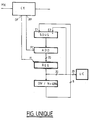
- FIG. single shows a load measuring circuit according to the invention.
- the measurement circuit includes a SUB subtractor, an ADD adder, a REG register and a divider-by-N DIV.
- This circuit is intended for measuring the load of the MX multiplex on which is mounted a CE cell multiplex alignment circuit.
- Such an alignment circuit is described in document EP-A-113 307. It is recalled that this alignment circuit delivers a signal DF of level "1" each time that it detects a cell start byte and a signal PP of level "1" each time the cell being treated is not empty.
- the clock input H of the register REG is connected to the output DF of the alignment circuit CE.
- the parallel signal input of the REG register is connected to the output of the adder ADD and its parallel signal output is connected to the signal input of the divider-by-N DIV.
- the REG register is a p- bit register and p has been chosen equal to 20.
- the output of the divider DIV is connected to the measurement output of the measurement circuit.
- the divider DIV divides the value of the content of the register REG by N, where N is, in the example described, chosen equal to 2 n .
- N is, in the example described, chosen equal to 2 n .
- the SOUS subtractor performs the subtraction of two operands: E2 minus E1. It has a first input to which the operand E2 is applied and which is connected to the parallel signal output of the register REG, a second input to which the operand E1 is applied and which is connected to the (pn) wires, i.e. eight wires, least significant of the REG register output signal.
- the output of the subtractor SUB is connected to the first input of the adder ADD, the second input of which is connected to the output PP of the alignment circuit CE.
- the content of the register REG is transmitted to the divider DIV and at the input E2, the division is made, then the subtraction and the addition, then the result of the addition is recorded in the REG register which keeps it until the next clock pulse.
- the value of the content of the register REG tends towards a value which corresponds to the load of the multiplex.
- the value of this charge referred to a maximum value equal to "1" is given, in binary form, by the integer part "0" followed by the twenty bits of the register REG, these bits corresponding to the decimal part of the charge.
- the processor CPU performs a sampling with a period of the order of a second, the frequency of knowledge of the load of the multiplex facilitates the admission of a new call and the management and maintenance operations.
- the useful cells of the multiplex have been taken into account in the ADD adder, regardless of their belonging to such or such such virtual circuit.
- this criterion can be provided by a memory (not shown) for analyzing the VCI (Virtual Channel Identifier, which translates to Virtual Circuit Identifier), the analysis memory existing in each switch and the corresponding criterion, by example, to the identifier contained in the header of the cell.
Landscapes
- Engineering & Computer Science (AREA)
- Computer Networks & Wireless Communication (AREA)
- Signal Processing (AREA)
- Data Exchanges In Wide-Area Networks (AREA)
- Use Of Switch Circuits For Exchanges And Methods Of Control Of Multiplex Exchanges (AREA)
Claims (8)
- Verfahren zur Messung der Belastung eines Multiplexers, insbesondere in einem Kommutationsnetz mit asynchronen Zellen oder Paketen, dadurch gekennzeichnet, daß bei jeder über den Multiplexer übertragenen Zelle ein Wert eingefügt wird, der durch eine vorbestimmte Zahl (N) geteilt wird, daß der Wert den ersten Operanden (E2) einer Subtraktion bildet und das Ergebnis der Division den zweiten Operanden (E1) der Subtraktion bildet, daß dem Ergebnis der Subtraktion ein fester vorbestimmter Wert hinzugefügt wird, wenn die übertragene Zelle in ihrem Kopfteil einen besonderen Identifikator und im gegenteiligen Fall einen Nullwert aufweist, und daß das Ergebnis der von der Addition gefolgten Subtraktion den neuen einzufügenden Wert bildet, der ebenso das Maß der Belastung darstellt.
- Verfahren nach Anspruch 1, dadurch gekennzeichnet, daß der Identifikator eine nicht leere Zelle identifiziert.
- Verfahren nach Anspruch 1 oder 2, dadurch gekennzeichnet, daß die vorbestimmte Zahl (N) kleiner als der maximale einzufügende Wert (2p) und der vorbestimmte feste Wert kleiner ist als die vorbestimmte Zahl (N).
- Verfahren nach einem der Ansprüche 1 - 3, dadurch gekennzeichnet, daß der eingefügte Wert eine binäre Zahl mit p Bit und die vorbestimmte Zahl (N) eine binäre Zahl mit n Bit ist, wobei n kleiner als p und der feste vorbestimmte Wert gleich 2(p-n) ist.
- Schaltung zur Durchführung des Verfahrens nach einem der Ansprüche 1 - 4 zum Messen der Belastung eines Multiplexers, insbesondere in einem Kommutationsnetz mit asynchronen Zellen oder Paketen, dadurch gekennzeichnet, daß die Schaltung einen Subtrahierer (SOUS) und einen Addierer (ADD), ein Register (REG) und einen Dividierer (DIV) enthält, daß der Takteingang (H) des Registers (REG) das Taktsignal der Zelle des Multiplexers empfängt, daß der Signaleingang des Registers (REG) mit dem Ausgang des Addierers (ADD) und der Signalausgang des Registers (REG) parallel mit dem Eingang des ersten Operanden (E2) des Subtrahierers (SOUS), mit dem Eingang des Dividierers (DIV) und mit dem Ausgang der Schaltung und der Ausgang des Dividierers (DIV) mit dem Eingang des zweiten Operanden (E1) des Subtrahierers (SOUS) und der Ausgang des Subtrahierers (SOUS) mit dem ersten Eingang des Addierers (ADD) verbunden ist, dessen zweiter Eingang ein den vorbestimmten festen Wert darstellendes Signal empfängt, wenn die laufende Zelle des Multiplexers in ihrem Kopfteil den besonderen Identifikator enthält, und in den anderen Fällen einen Nullwert, wobei der Ausgang des Addierers (ADD) mit dem Eingang des Registers (REG) verbunden ist.
- Schaltung nach Anspruch 5, dadurch gekennzeichnet, daß das den verbestimmten festen Wert darstellende Signal das Signal ist, welches anzeigt, daß die Zelle nicht leer ist.
- Schaltung nach Anspruch 6, dadurch gekennzeichnet, daß der Takteingang (H) des Registers (REG) mit dem Ausgang der Taktzelle (DF) einer Schaltung zum Aneinanderreihen (CE) verbunden ist, die in Reihe mit dem Multiplexer (MX) geschaltet ist, wobei der zweite Eingang des Addierers (ADD) mit dem Ausgang (PC) für die Anwesenheit der nicht leeren Zelle der Schaltung zum Aneinanderreihen (CE) verbunden ist.
- Schaltung nach einem der Ansprüche 5 - 7, dadurch gekennzeichnet, daß der Ausgang des Registers (REG) mit einem Eingang eines Prozessors (UC) verbunden ist, der eine periodische Abtastung des Wertes der Belastungsmessung ermöglicht.
Applications Claiming Priority (2)
| Application Number | Priority Date | Filing Date | Title |
|---|---|---|---|
| FR9006828A FR2662886B1 (fr) | 1990-05-29 | 1990-05-29 | Methode de mesure de la charge d'un multiplex et circuit pour sa mise en óoeuvre. |
| FR9006828 | 1990-05-29 |
Publications (2)
| Publication Number | Publication Date |
|---|---|
| EP0459927A1 EP0459927A1 (de) | 1991-12-04 |
| EP0459927B1 true EP0459927B1 (de) | 1994-10-19 |
Family
ID=9397175
Family Applications (1)
| Application Number | Title | Priority Date | Filing Date |
|---|---|---|---|
| EP91460031A Expired - Lifetime EP0459927B1 (de) | 1990-05-29 | 1991-05-24 | Verfahren zur Messung der Belastung eines Multiplexers sowie Schaltung zur Durchführung des Verfahrens |
Country Status (6)
| Country | Link |
|---|---|
| US (1) | US5233601A (de) |
| EP (1) | EP0459927B1 (de) |
| JP (1) | JP3070991B2 (de) |
| DE (1) | DE69104649T2 (de) |
| ES (1) | ES2062732T3 (de) |
| FR (1) | FR2662886B1 (de) |
Families Citing this family (3)
| Publication number | Priority date | Publication date | Assignee | Title |
|---|---|---|---|---|
| FR2674084B1 (fr) * | 1991-03-13 | 1993-12-24 | Michel Servel | Dispositif de declenchement de temporisations multiples. |
| EP0576750B1 (de) * | 1992-06-30 | 1998-09-09 | Siemens Aktiengesellschaft | Modifiziertes Leaky-Bucket-Verfahren |
| US7676492B2 (en) * | 2006-04-07 | 2010-03-09 | International Business Machines Corporation | Migration of database using serialized objects |
Family Cites Families (8)
| Publication number | Priority date | Publication date | Assignee | Title |
|---|---|---|---|---|
| DE310173C (de) * | ||||
| FR2538976A1 (fr) * | 1982-12-29 | 1984-07-06 | Servel Michel | Systeme de commutation de paquets synchrones de longueur fixe |
| FR2616024B1 (fr) * | 1987-05-26 | 1989-07-21 | Quinquis Jean Paul | Systeme et methode de controle de flux de paquets |
| FR2616025B1 (fr) * | 1987-05-26 | 1989-07-21 | Lespagnol Albert | Methode et systeme de controle de flux de paquets |
| DE3732937A1 (de) * | 1987-09-30 | 1989-04-20 | Philips Patentverwaltung | Schaltungsanordnung zur vermeidung von ueberlast in einem breitband-vermittlungssystem |
| WO1990000331A1 (en) * | 1988-06-30 | 1990-01-11 | Alcatel N.V. | Statistical measurement equipment and communication system using same |
| SE462360B (sv) * | 1988-10-28 | 1990-06-11 | Ellemtel Utvecklings Ab | Foerfarande och anordning foer att foerhindra att det paa en gemensam oeverfoeringslaenk saends datapaket med hoegre intensitet aen ettfoerutbestaemt vaerdesitet aen ett foerutbestaemt vaerde |
| FR2643532B1 (fr) * | 1989-02-17 | 1991-05-10 | France Etat | Procede de reservation de debits et commutateurs temporels de paquets asynchrones |
-
1990
- 1990-05-29 FR FR9006828A patent/FR2662886B1/fr not_active Expired - Lifetime
-
1991
- 1991-05-17 US US07/703,475 patent/US5233601A/en not_active Expired - Lifetime
- 1991-05-24 DE DE69104649T patent/DE69104649T2/de not_active Expired - Lifetime
- 1991-05-24 ES ES91460031T patent/ES2062732T3/es not_active Expired - Lifetime
- 1991-05-24 EP EP91460031A patent/EP0459927B1/de not_active Expired - Lifetime
- 1991-05-29 JP JP22813491A patent/JP3070991B2/ja not_active Expired - Fee Related
Also Published As
| Publication number | Publication date |
|---|---|
| DE69104649D1 (de) | 1994-11-24 |
| FR2662886A1 (fr) | 1991-12-06 |
| DE69104649T2 (de) | 1995-03-02 |
| JP3070991B2 (ja) | 2000-07-31 |
| EP0459927A1 (de) | 1991-12-04 |
| FR2662886B1 (fr) | 1992-08-14 |
| JPH0730542A (ja) | 1995-01-31 |
| ES2062732T3 (es) | 1994-12-16 |
| US5233601A (en) | 1993-08-03 |
Similar Documents
| Publication | Publication Date | Title |
|---|---|---|
| Kamitake et al. | Evaluation of an admission control scheme for an ATM network considering fluctuations in cell loss rate | |
| US6625155B1 (en) | Model-based admission control adjustment in data networks | |
| EP0162174B1 (de) | Puffereinrichtung für ein Sprachübertragungsnetzwerk | |
| FR2797369A1 (fr) | Recepteur optique independant du debit de bits et procede pour celui-ci | |
| EP0490440B1 (de) | Anordnung zur Übertragung von mehreren Kanälen mit verschiedenen Bitraten über einer zeitmultiplexierten Übertragungsstrecke | |
| EP0383660B1 (de) | Ratenreservierung in einem asynchronen Paketnetzwerk | |
| US20090238575A1 (en) | Ultra high-speed adaptive and all-optical method for data packet rate multiplication compatible with multiple data rates | |
| EP0112953A1 (de) | Verfahren zur dynamischen Zuweisung von Geschwindigkeiten in einem Multiplexübertragungssystem | |
| US6628612B1 (en) | Derivation of equivalent bandwidth of an information flow | |
| EP0693841A1 (de) | Bandbreitenreservierung in Vermittlungsstellen eines asynchronen Netzes | |
| EP0459927A1 (de) | Verfahren zur Messung der Belastung eines Multiplexers sowie Schaltung zur Durchführung des Verfahrens | |
| US6570694B1 (en) | System and method for low-jitter asynchronous optical regeneration using wavelength sampling | |
| EP0658994B1 (de) | Verfahren und Vorrichtung zur Feinsynchronisation von ATM-Zellen in einem optischen ATM-Knoten | |
| EP0612172B1 (de) | Optisch-elektronische Satellitenzentrale zur Verbindung von optischen Teilnehmerleitungen an ein ATM-Netz | |
| EP0874533A1 (de) | Gleichmässige Paketenablauffolgeplanung | |
| Harb | Performance evaluation of OBS WDM core node using queuing theory | |
| EP2606655B1 (de) | Verfahren zur umschaltung eines optischen datenstroms, computerprogrammprodukt sowie zugehörige speichervorrichtung und knoten | |
| Callegati | Which packet length for a transparent optical network? | |
| FR2685592A1 (fr) | Procede et un systeme de transmission d'information sur une liaison de transmission par blocs de donnees de longueur variable en multiplexage temporel de type asynchrone. | |
| EP0605267B1 (de) | Rahmen mit mehreren Übertragungsraten und Anordnung zur Multiplexierung von nicht-ganzzahligen Bitraten | |
| Guillemot et al. | KEOPS optical packet switch demonstrator: architecture and testbed performance | |
| Rogiest et al. | Quantifying the impact of wavelength conversion on the performance of fiber delay line buffers | |
| EP0981879B1 (de) | Verfahren und vorrichtung zur kontrolle der bitratenkonformität von datumzellen | |
| Shuaib et al. | Empirical evaluation of ATM CBR traffic transported under diverse operating conditions | |
| KR0168232B1 (ko) | 광대역종합정보통신망용 비동기전송모드 교환기내 멀티플렉서의 버퍼관리 블럭 설계 방법 |
Legal Events
| Date | Code | Title | Description |
|---|---|---|---|
| PUAI | Public reference made under article 153(3) epc to a published international application that has entered the european phase |
Free format text: ORIGINAL CODE: 0009012 |
|
| AK | Designated contracting states |
Kind code of ref document: A1 Designated state(s): DE ES GB IT |
|
| 17P | Request for examination filed |
Effective date: 19920408 |
|
| 17Q | First examination report despatched |
Effective date: 19940322 |
|
| GRAA | (expected) grant |
Free format text: ORIGINAL CODE: 0009210 |
|
| ITF | It: translation for a ep patent filed | ||
| AK | Designated contracting states |
Kind code of ref document: B1 Designated state(s): DE ES GB IT |
|
| REF | Corresponds to: |
Ref document number: 69104649 Country of ref document: DE Date of ref document: 19941124 |
|
| GBT | Gb: translation of ep patent filed (gb section 77(6)(a)/1977) |
Effective date: 19941103 |
|
| REG | Reference to a national code |
Ref country code: ES Ref legal event code: FG2A Ref document number: 2062732 Country of ref document: ES Kind code of ref document: T3 |
|
| PLBE | No opposition filed within time limit |
Free format text: ORIGINAL CODE: 0009261 |
|
| STAA | Information on the status of an ep patent application or granted ep patent |
Free format text: STATUS: NO OPPOSITION FILED WITHIN TIME LIMIT |
|
| 26N | No opposition filed | ||
| REG | Reference to a national code |
Ref country code: GB Ref legal event code: IF02 |
|
| PGFP | Annual fee paid to national office [announced via postgrant information from national office to epo] |
Ref country code: ES Payment date: 20100511 Year of fee payment: 20 |
|
| PGFP | Annual fee paid to national office [announced via postgrant information from national office to epo] |
Ref country code: DE Payment date: 20100428 Year of fee payment: 20 Ref country code: IT Payment date: 20100503 Year of fee payment: 20 |
|
| PGFP | Annual fee paid to national office [announced via postgrant information from national office to epo] |
Ref country code: GB Payment date: 20100429 Year of fee payment: 20 |
|
| REG | Reference to a national code |
Ref country code: DE Ref legal event code: R071 Ref document number: 69104649 Country of ref document: DE |
|
| REG | Reference to a national code |
Ref country code: GB Ref legal event code: PE20 Expiry date: 20110523 |
|
| PG25 | Lapsed in a contracting state [announced via postgrant information from national office to epo] |
Ref country code: GB Free format text: LAPSE BECAUSE OF EXPIRATION OF PROTECTION Effective date: 20110523 |
|
| REG | Reference to a national code |
Ref country code: ES Ref legal event code: FD2A Effective date: 20120110 |
|
| PG25 | Lapsed in a contracting state [announced via postgrant information from national office to epo] |
Ref country code: ES Free format text: LAPSE BECAUSE OF EXPIRATION OF PROTECTION Effective date: 20110525 |
|
| PG25 | Lapsed in a contracting state [announced via postgrant information from national office to epo] |
Ref country code: DE Free format text: LAPSE BECAUSE OF EXPIRATION OF PROTECTION Effective date: 20110525 |