EP0459618B1 - Polycrystalline silicon resistors for integrated circuits - Google Patents
Polycrystalline silicon resistors for integrated circuits Download PDFInfo
- Publication number
- EP0459618B1 EP0459618B1 EP91303596A EP91303596A EP0459618B1 EP 0459618 B1 EP0459618 B1 EP 0459618B1 EP 91303596 A EP91303596 A EP 91303596A EP 91303596 A EP91303596 A EP 91303596A EP 0459618 B1 EP0459618 B1 EP 0459618B1
- Authority
- EP
- European Patent Office
- Prior art keywords
- polycrystalline silicon
- region
- resistor
- layer
- insulating layer
- Prior art date
- Legal status (The legal status is an assumption and is not a legal conclusion. Google has not performed a legal analysis and makes no representation as to the accuracy of the status listed.)
- Expired - Lifetime
Links
Images


Classifications
-
- H—ELECTRICITY
- H10—SEMICONDUCTOR DEVICES; ELECTRIC SOLID-STATE DEVICES NOT OTHERWISE PROVIDED FOR
- H10D—INORGANIC ELECTRIC SEMICONDUCTOR DEVICES
- H10D84/00—Integrated devices formed in or on semiconductor substrates that comprise only semiconducting layers, e.g. on Si wafers or on GaAs-on-Si wafers
-
- H—ELECTRICITY
- H10—SEMICONDUCTOR DEVICES; ELECTRIC SOLID-STATE DEVICES NOT OTHERWISE PROVIDED FOR
- H10D—INORGANIC ELECTRIC SEMICONDUCTOR DEVICES
- H10D1/00—Resistors, capacitors or inductors
- H10D1/40—Resistors
- H10D1/47—Resistors having no potential barriers
-
- H—ELECTRICITY
- H10—SEMICONDUCTOR DEVICES; ELECTRIC SOLID-STATE DEVICES NOT OTHERWISE PROVIDED FOR
- H10B—ELECTRONIC MEMORY DEVICES
- H10B10/00—Static random access memory [SRAM] devices
-
- H—ELECTRICITY
- H10—SEMICONDUCTOR DEVICES; ELECTRIC SOLID-STATE DEVICES NOT OTHERWISE PROVIDED FOR
- H10B—ELECTRONIC MEMORY DEVICES
- H10B10/00—Static random access memory [SRAM] devices
- H10B10/15—Static random access memory [SRAM] devices comprising a resistor load element
Definitions
- the present invention relates generally to integrated circuits, and more specifically to a method for fabricating polycrystalline silicon resistor structures therein.
- IBM Tech Disclosure Bulletin Vol 26, No 2, July 1983 pages 623-625 relates to a process for making high value polysilicon resistors.
- a silicon dioxide layer is formed over an insulating layer. Rectangular windows are etched in the SiO 2 layer using a mask.
- a layer of doped poly is deposited, and a blanket RIE is used to form sidewalls. The sidewalls form the body of the resistor.
- CMOS SRAMs often use a four transistor cell design having resistive load devices. This design is used in order to save chip layout area over the traditional six transistor cell design. Two N-channel transistors are used to form a cross-coupled latch, while two additional N-channel transistors are used to provide access to the cell for reading and writing data. Two load devices are connected between the N-channel transistors in the latch and the power supply.
- the resistive load devices are formed after formation of the transistors. After the transistors have been formed, a dielectric layer is deposited and contact openings are formed to the substrate. A second polycrystalline silicon layer is deposited and lightly doped N-type to achieve a resistivity in the range of 10 6 to 10 13 ohms/square. This blanket implant determines the load resistor value.
- the resistivity of the load resistors must be low enough to supply ample current to compensate for transistor leakages, but high enough to allow for sufficient standby currents for proper device operation under adverse conditions.
- Resistance of the polycrystalline silicon load structures is a function of four variables. These are: the grain structure of the polycrystalline silicon used to form the resistor structure, the impurity levels used to dope the polycrystalline silicon; the cross-sectional area of the resistive device; and the length of the device. Impurity levels and polycrystalline silicon grain structure can be controlled only to limits determined by the process technology being used. If cross-sectional area of the structure could be reduced, length of the load resistor could also be reduced to preserve a given resistance for a small overall structure.
- a method for fabricating polycrystalline silicon resistor structure includes steps directed to the provision of a polycrystalline silicon structure having a decreased width. Sidewall spacers are used to narrow a region in which the polycrystalline silicon resistors are formed. This technique provides a reduced cross-section for the resistor structures, allowing shorter resistors to be used, or providing increased resistance for longer resistors.
- a method for fabricating a resistor structure in an integrated circuit device comprising the steps of:
- an integrated circuit device structure comprising: an insulating layer having a resistor structure region between two contact regions, said resistor structure region having substantially vertical side walls; insulating side wall regions along the side walls of the resistor structure region, defining a narrowed region therebetween; and a polycrystalline silicon region located in the narrowed region, wherein said polycrystalline silicon region forms a resistor.
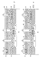
- integrated circuit devices are formed in a substrate 10.
- Field oxide regions 12, 14 separate and define active areas within the substrate 10.
- Polycrystalline silicon signal line 16 is used to conduct signals on the device.
- Signal line 16 is separated from the substrate 10 by gate oxide layer 18.
- Sidewall oxide spacers 20 are formed on either side of the signal line 16 as known in the art.
- signal line 16 can be a non-gate signal line which is utilized in a shared contact region.
- Signal line 16 will be so used as will be described further below.
- Active regions 22, 24 function as the source/drain regions of the field effect device if polycrystalline silicon signal line 16 actually functions as a field effect gate. In a shared contact layout, the active areas 22, 24 may actually be connected out of the plane of the drawing, so that the signal line 16 does not function as a gate.
- Polycrystalline silicon signal line 26 rests on field oxide region 14 .
- Oxide sidewall spacers 28 are formed thereon at the same time as sidewall spacers 20 .
- dielectric layer 30 is deposited over the surface of the integrated circuit device.
- This layer 30 is preferably LPCVD/APCVD/LTO silicon dioxide followed by a deposited layer of LPCVD silicon nitride as known in the art.
- Other insulating layers may be used if desired.
- insulating layer 32 is deposited over the surface of the device.
- Layer 32 is preferably a dielectric which can be easily planarized.
- Layer 32 may be a reflow glass, for example, BPSG which is deposited and heated to reflow as known in the art. If BPSG is used, the reflow is preferably performed in an ambient atmosphere including steam. The reflow cycle, or other planarization step, results in a near planar surface as shown in Figure 1.
- an insulating layer 34 is deposited over the surface of the device.
- Insulating layer 34 is preferably an LPCVD silicon nitride layer deposited to a depth of approximately 2000-4000 angstroms.
- Nitride layer 34 is then patterned and etched to define a region 36 in which polycrystalline silicon resistors are to be formed.
- the insulating layer used to form the spacers 38 may be an oxide layer and is preferably an LPCVD/LTO silicon oxide layer.
- the oxide layer is deposited to a thickness which results in the width of the oxide regions 38 resulting as desired.
- the width of the spacers 38 is approximately equal to the thickness of the oxide layer from which they are formed.
- the oxide layer used to produce spacers 38 is deposited to a depth of approximately 4000 angstroms.
- contacts are opened to the substrate 10 and other underlying features through insulating layers 30, 32 , 34 .
- contact opening 40 makes contact with active region 22 within a substrate 10 .
- Contact opening 42 makes contact with both the polycrystalline silicon signal line 16 and active region 24 .
- the contact to be formed in opening 42 is part of a shared contact region.
- Contact opening 44 is opened simply to allow contact to underlying polycrystalline silicon line 26 .
- a layer of polycrystalline silicon 46 is deposited over the device.
- Layer 46 is preferably deposited to a depth of approximately 500 to 1500 angstroms.
- a blanket impurity implant is then made to control the resistivity of the polycrystalline silicon resistors to be fabricated in region 36. If N-type resistors are to be formed, an N - implant is made.
- the polycrystalline silicon layer 46 is patterned and etched to remove it except in the desired contact regions 40, 42, 44 and interconnect regions as desired. This results in various polycrystalline silicon contact structures 48 as shown.
- the layer 46 is etched to completely clear it, which can be accomplished by etching until the end point is reached as known in the art, and continuing the etch for a period of time approximately ten percent beyond reaching the end point Such an over etch insures that undesired polycrystalline silicon regions do not remain behind.
- resistor region 36 is left unmasked. This causes the polycrystalline silicon overlying such region 36 to be etched away. However, due to the depth of the region 36 , some material remains in the region between the sidewall spacers 38 .
- This polycrystalline silicon region 50 provides the resistor desired for use in the device. As will be apparent to those skilled in the art, the cross-sectional area of resistor 50 is much smaller than a resistor which fills the resistor region 36 .
- a masked N + implant can then be made to reduce the resistivity of the polycrystalline silicon contacts and interconnect 48 .
- Remaining fabrication steps for the device, such as formation of further polycrystalline silicon and metal interconnect layers, is completed in a conventional manner. To a great extent, the device is already planarized due to the planarization of insulating layer 32 , so that further planarization steps may be minimized or not required.
- FIG. 5 an alternative technique for fabricating small cross-section polycrystalline silicon resistor structures is shown. This technique does not form part of the invention as claimed.
- the technique used is very similar to that described in connection with Figures 1 - 4 . The difference is that the deposition of the oxide layer, and anisotropic etching thereof to form sidewall spacers 38 , is not performed. Instead, when polycrystalline silicon layer 46 is deposited over the device, it extends across the entire width of resistor region 36 . When the polycrystalline silicon is anisotropically etched to form contact and interconnect regions 48 , sidewall polycrystalline silicon regions 52 are formed within the resistor region 36 . These regions 52 are separated by region 54 in much the same manner that sidewall oxide regions 38 were separated as described in connection with Figure 2 .
- the width of the polycrystalline silicon resistors 52 is controlled by the depth to which polycrystalline silicon layer 46 is deposited.
- the height of the resistor regions 52 is controlled by the depth to which the nitride layer 34 is deposited. Decreasing the depth of nitride layer 34 , or the thickness of polycrystalline silicon layer 46 , results in resistor regions 52 having a smaller cross-sectional area
- Figure 6 illustrates a plan view of a polycrystalline silicon resistor formed according to the techniques described in connection with Figures 14 .
- Polycrystalline silicon contacts 60 connect to signal lines 62 .
- Lines 64 indicate the boundaries of the resistor region 36 .
- Polycrystalline silicon resistor 66 connects the contacts 60 .
- the cross-sectional area of the polycrystalline silicon resistor 66 is greatly reduced from that which would normally be formed connecting contact regions 60 . This allows a much higher valued resistor to be formed, or a shorter resistor to be used. Use of shorter resistor 66 allows the contacts 60 to be placed closer together, if desired, thereby reducing the overall layout area required for circuit structures such as 4-transistor SRAM cells.
- Figure 7 is a plan view of a device constructed according to the method described in connection with Figure 5 . This devices does not form part of the invention as claimed. Contact regions 70 are connected to signal lines 72 . Polycrystalline silicon resistors 74 connect the contact regions 70 . Since the resistors are formed on both sidewalls of the resistor region 36 , two parallel resistors 74 are formed. The twin resistor structures 74 shown in Figure 7 have the same advantages as the single structure 66 shown in Figure 6 , and can be fabricated with a lesser number of process steps.
- the resistor structures described above provide polycrystalline silicon resistor structures which have a reduced width, and thus a reduced cross-sectional area Use of such resistor structures in circuits such as CMOS SRAM cells allows the use of shorter resistors for a given required resistance. This can lead to smaller cell layout areas, and increased device density on an integrated circuit chip.
Landscapes
- Semiconductor Integrated Circuits (AREA)
- Internal Circuitry In Semiconductor Integrated Circuit Devices (AREA)
Description
Claims (10)
- A method for fabricating a resistor structure (50,66) in an integrated circuit device, comprising the steps of:forming a first insulating layer (34) over the device;patterning the first insulating layer (34) to define a resistor structure region (36) for formation of the resistor structure;forming a second insulating layer over the device;anisotropically etching the second insulating layer, leaving insulating sidewalls (38) in the resistor structure region, wherein a narrowed resistor structure region is defined;depositing a layer of polycrystalline silicon (46) over the device; andanisotropically etching the polycrystalline silicon layer (46), wherein polycrystalline silicon remains in the narrowed resistor structure region to form a resistor structure (50,66).
- The method of claim 1, further comprising the step of:
before said polycrystalline silicon etching step, masking portions of the polycrystalline silicon layer (46) to protect selected regions thereof, leaving the resistor structure region unmasked, wherein the selected regions of the polycrystalline silicon layer (48) are protected from etching during the polycrystalline silicon etching step. - The method of claim 2, further comprising the step of:
before said polycrystalline silicon deposition step, etching contacts (40) to underlying circuit structures, wherein the contacts (40), after the polysilicon deposition step, will be masked so as to be included in the selected regions (48). - The method of claim 1, wherein the first insulating layer (34) comprises silicon nitride.
- The method of claim 1, wherein the second insulating layer comprises a deposited oxide.
- The method of claim 1, further comprising the step of:
prior to said first insulating layer forming step, planarizing a surface of the integrated circuit device. - The method of claim 6, wherein said planarizing step comprises the steps of:depositing a layer of reflowable glass (32) over the device; andheating the device to a temperature sufficient to cause the glass layer to flow into a relatively planar layer (32).
- The method of claim 7, wherein the reflowable glass comprises BPSG.
- An integrated circuit device structure, comprising:an insulating layer (34) having a resistor structure region (36) between two contact regions (60) said resistor structure region (36) having substantially vertical side walls;insulating side wall regions (38) along the side walls of the resistor structure region (36), defining a narrowed region therebetween; anda polycrystalline silicon region (50) located in the narrowed region, wherein said polycrystalline silicon region (50) forms a resistor( 50,66).
- The structure of claim 9, wherein the resistor comprises a load structure for an SRAM cell.
Applications Claiming Priority (2)
| Application Number | Priority Date | Filing Date | Title |
|---|---|---|---|
| US531012 | 1990-05-31 | ||
| US07/531,012 US5151376A (en) | 1990-05-31 | 1990-05-31 | Method of making polycrystalline silicon resistors for integrated circuits |
Publications (3)
| Publication Number | Publication Date |
|---|---|
| EP0459618A2 EP0459618A2 (en) | 1991-12-04 |
| EP0459618A3 EP0459618A3 (en) | 1994-01-19 |
| EP0459618B1 true EP0459618B1 (en) | 1998-12-02 |
Family
ID=24115894
Family Applications (1)
| Application Number | Title | Priority Date | Filing Date |
|---|---|---|---|
| EP91303596A Expired - Lifetime EP0459618B1 (en) | 1990-05-31 | 1991-04-22 | Polycrystalline silicon resistors for integrated circuits |
Country Status (5)
| Country | Link |
|---|---|
| US (2) | US5151376A (en) |
| EP (1) | EP0459618B1 (en) |
| JP (1) | JP3418410B2 (en) |
| KR (1) | KR100231020B1 (en) |
| DE (1) | DE69130547T2 (en) |
Families Citing this family (15)
| Publication number | Priority date | Publication date | Assignee | Title |
|---|---|---|---|---|
| US5196233A (en) * | 1989-01-18 | 1993-03-23 | Sgs-Thomson Microelectronics, Inc. | Method for fabricating semiconductor circuits |
| US5151387A (en) | 1990-04-30 | 1992-09-29 | Sgs-Thomson Microelectronics, Inc. | Polycrystalline silicon contact structure |
| JPH0541378A (en) * | 1991-03-15 | 1993-02-19 | Mitsubishi Electric Corp | Semiconductor device and manufacturing method thereof |
| US5424570A (en) * | 1992-01-31 | 1995-06-13 | Sgs-Thomson Microelectronics, Inc. | Contact structure for improving photoresist adhesion on a dielectric layer |
| KR940008883B1 (en) * | 1992-04-08 | 1994-09-28 | 삼성전자 주식회사 | Manufacturing method of thin film resistor |
| US6037623A (en) * | 1992-04-16 | 2000-03-14 | Stmicroelectronics, Inc. | Polycrystalline silicon resistors for integrated circuits |
| US5538915A (en) * | 1992-06-05 | 1996-07-23 | The Regents Of The University Of California | Process for forming synapses in neural networks and resistor therefor |
| US5395785A (en) * | 1993-12-17 | 1995-03-07 | Sgs-Thomson Microelectronics, Inc. | SRAM cell fabrication with interlevel dielectric planarization |
| US5545581A (en) * | 1994-12-06 | 1996-08-13 | International Business Machines Corporation | Plug strap process utilizing selective nitride and oxide etches |
| US5635418A (en) * | 1995-03-23 | 1997-06-03 | Micron Technology, Inc. | Method of making a resistor |
| US5723352A (en) * | 1995-08-03 | 1998-03-03 | Taiwan Semiconductor Manufacturing Company | Process to optimize performance and reliability of MOSFET devices |
| US6013931A (en) * | 1997-03-25 | 2000-01-11 | Kabushiki Kaisha Toshiba | Semiconductor device and method for producing the same |
| US6140684A (en) * | 1997-06-24 | 2000-10-31 | Stmicroelectronic, Inc. | SRAM cell structure with dielectric sidewall spacers and drain and channel regions defined along sidewall spacers |
| JPH11317527A (en) | 1998-05-06 | 1999-11-16 | Mitsubishi Electric Corp | Semiconductor device and manufacturing method thereof |
| KR100464941B1 (en) * | 1998-12-24 | 2005-04-06 | 주식회사 하이닉스반도체 | Full CMOS SRAM Cell Manufacturing Method |
Family Cites Families (15)
| Publication number | Priority date | Publication date | Assignee | Title |
|---|---|---|---|---|
| JPS5267532A (en) * | 1975-12-03 | 1977-06-04 | Nippon Telegr & Teleph Corp <Ntt> | Semiconductor memory unit |
| US4110776A (en) * | 1976-09-27 | 1978-08-29 | Texas Instruments Incorporated | Semiconductor integrated circuit with implanted resistor element in polycrystalline silicon layer |
| IT1094517B (en) * | 1978-04-28 | 1985-08-02 | Componenti Elettronici Sgs Ate | PROCEDURE FOR THE MANUFACTURE OF A FILIFORM RESISTIVE ELEMENT FOR INTEGRATED CIRCUIT |
| US4464212A (en) * | 1982-12-13 | 1984-08-07 | International Business Machines Corporation | Method for making high sheet resistivity resistors |
| JPS59155128A (en) * | 1983-02-23 | 1984-09-04 | Mitsubishi Electric Corp | Manufacture of semiconductor device |
| JPS60236257A (en) * | 1984-05-09 | 1985-11-25 | Matsushita Electric Ind Co Ltd | Semiconductor device |
| JPS61164241A (en) * | 1985-01-16 | 1986-07-24 | Nec Corp | Semiconductor device |
| JPS61168955A (en) * | 1985-01-22 | 1986-07-30 | Nec Corp | semiconductor equipment |
| US4774203A (en) * | 1985-10-25 | 1988-09-27 | Hitachi, Ltd. | Method for making static random-access memory device |
| JPS62285462A (en) * | 1986-06-03 | 1987-12-11 | Sony Corp | Semiconductor device |
| JPS63136668A (en) * | 1986-11-28 | 1988-06-08 | Fuji Electric Co Ltd | Manufacture of semiconductor device |
| JPS6469031A (en) * | 1987-09-10 | 1989-03-15 | Matsushita Electronics Corp | Manufacture of semiconductor device |
| US4835589A (en) * | 1987-09-28 | 1989-05-30 | Motorola, Inc. | Ram cell having trench sidewall load |
| JPH01152662A (en) * | 1987-12-09 | 1989-06-15 | Fujitsu Ltd | Semiconductor memory |
| JP2913404B2 (en) * | 1988-06-28 | 1999-06-28 | コニカ株式会社 | Radiation image information reading apparatus and radiation image information reading method |
-
1990
- 1990-05-31 US US07/531,012 patent/US5151376A/en not_active Expired - Lifetime
-
1991
- 1991-04-22 DE DE69130547T patent/DE69130547T2/en not_active Expired - Fee Related
- 1991-04-22 EP EP91303596A patent/EP0459618B1/en not_active Expired - Lifetime
- 1991-05-30 JP JP12640891A patent/JP3418410B2/en not_active Expired - Fee Related
- 1991-05-31 KR KR1019910009132A patent/KR100231020B1/en not_active Expired - Fee Related
-
1992
- 1992-04-16 US US07/869,517 patent/US5825060A/en not_active Expired - Lifetime
Also Published As
| Publication number | Publication date |
|---|---|
| US5825060A (en) | 1998-10-20 |
| JP3418410B2 (en) | 2003-06-23 |
| KR100231020B1 (en) | 1999-11-15 |
| KR910020892A (en) | 1991-12-20 |
| EP0459618A2 (en) | 1991-12-04 |
| EP0459618A3 (en) | 1994-01-19 |
| US5151376A (en) | 1992-09-29 |
| DE69130547D1 (en) | 1999-01-14 |
| DE69130547T2 (en) | 1999-04-29 |
| JPH04230069A (en) | 1992-08-19 |
Similar Documents
| Publication | Publication Date | Title |
|---|---|---|
| US5739564A (en) | Semiconductor device having a static-random-access memory cell | |
| US5485420A (en) | Static-random-access memory cell and an integrated circuit having a static-random-access memory cell | |
| US5122846A (en) | Bistable logic device using trench transistors | |
| EP0460833B1 (en) | Method of fabricating a field effect device with polycrystaline silicon channel | |
| US5151376A (en) | Method of making polycrystalline silicon resistors for integrated circuits | |
| US6277720B1 (en) | Silicon nitride dopant diffusion barrier in integrated circuits | |
| US6143615A (en) | Method of forming a resistor | |
| US5348901A (en) | Interconnect and resistor for integrated circuits | |
| US4673969A (en) | Semiconductor device having multiple conductive layers and the method of manufacturing the semiconductor device | |
| US5462894A (en) | Method for fabricating a polycrystalline silicon resistive load element in an integrated circuit | |
| US4987092A (en) | Process for manufacturing stacked semiconductor devices | |
| US5461000A (en) | Method of manufacturing dielectric as load resistor in 4T SRAM | |
| US5068201A (en) | Method for forming a high valued resistive load element and low resistance interconnect for integrated circuits | |
| US5770892A (en) | Field effect device with polycrystalline silicon channel | |
| KR100394126B1 (en) | Semiconductor device and method of manufacturing the same | |
| US5323045A (en) | Semiconductor SRAM with low resistance power line | |
| US6037623A (en) | Polycrystalline silicon resistors for integrated circuits | |
| US5268325A (en) | Method for fabricating a polycrystalline silicon resistive load element in an integrated circuit | |
| US5994180A (en) | Method of making SRAM having part of load resistance layer functions as power supply line | |
| US5027186A (en) | Semiconductor device | |
| US5075761A (en) | Local interconnect for integrated circuits | |
| KR960015786B1 (en) | Semiconductor device and fabricating method thereof | |
| KR100318319B1 (en) | Manufacturing Method for Cell of Semiconductor Memory Device | |
| KR19990050111A (en) | Load resistance formation method of SRAM cell | |
| JPH03248558A (en) | Semiconductor memory |
Legal Events
| Date | Code | Title | Description |
|---|---|---|---|
| PUAI | Public reference made under article 153(3) epc to a published international application that has entered the european phase |
Free format text: ORIGINAL CODE: 0009012 |
|
| AK | Designated contracting states |
Kind code of ref document: A2 Designated state(s): DE FR GB IT |
|
| PUAL | Search report despatched |
Free format text: ORIGINAL CODE: 0009013 |
|
| AK | Designated contracting states |
Kind code of ref document: A3 Designated state(s): DE FR GB IT |
|
| 17P | Request for examination filed |
Effective date: 19940707 |
|
| 17Q | First examination report despatched |
Effective date: 19950926 |
|
| GRAG | Despatch of communication of intention to grant |
Free format text: ORIGINAL CODE: EPIDOS AGRA |
|
| GRAG | Despatch of communication of intention to grant |
Free format text: ORIGINAL CODE: EPIDOS AGRA |
|
| GRAG | Despatch of communication of intention to grant |
Free format text: ORIGINAL CODE: EPIDOS AGRA |
|
| GRAH | Despatch of communication of intention to grant a patent |
Free format text: ORIGINAL CODE: EPIDOS IGRA |
|
| GRAH | Despatch of communication of intention to grant a patent |
Free format text: ORIGINAL CODE: EPIDOS IGRA |
|
| GRAH | Despatch of communication of intention to grant a patent |
Free format text: ORIGINAL CODE: EPIDOS IGRA |
|
| GRAA | (expected) grant |
Free format text: ORIGINAL CODE: 0009210 |
|
| RAP1 | Party data changed (applicant data changed or rights of an application transferred) |
Owner name: STMICROELECTRONICS, INC. |
|
| AK | Designated contracting states |
Kind code of ref document: B1 Designated state(s): DE FR GB IT |
|
| REF | Corresponds to: |
Ref document number: 69130547 Country of ref document: DE Date of ref document: 19990114 |
|
| ITF | It: translation for a ep patent filed | ||
| ET | Fr: translation filed | ||
| PLBE | No opposition filed within time limit |
Free format text: ORIGINAL CODE: 0009261 |
|
| STAA | Information on the status of an ep patent application or granted ep patent |
Free format text: STATUS: NO OPPOSITION FILED WITHIN TIME LIMIT |
|
| 26N | No opposition filed | ||
| PG25 | Lapsed in a contracting state [announced via postgrant information from national office to epo] |
Ref country code: DE Free format text: LAPSE BECAUSE OF NON-PAYMENT OF DUE FEES Effective date: 20000201 |
|
| REG | Reference to a national code |
Ref country code: GB Ref legal event code: IF02 |
|
| PGFP | Annual fee paid to national office [announced via postgrant information from national office to epo] |
Ref country code: FR Payment date: 20050408 Year of fee payment: 15 |
|
| PGFP | Annual fee paid to national office [announced via postgrant information from national office to epo] |
Ref country code: GB Payment date: 20050420 Year of fee payment: 15 |
|
| PG25 | Lapsed in a contracting state [announced via postgrant information from national office to epo] |
Ref country code: IT Free format text: LAPSE BECAUSE OF NON-PAYMENT OF DUE FEES;WARNING: LAPSES OF ITALIAN PATENTS WITH EFFECTIVE DATE BEFORE 2007 MAY HAVE OCCURRED AT ANY TIME BEFORE 2007. THE CORRECT EFFECTIVE DATE MAY BE DIFFERENT FROM THE ONE RECORDED. Effective date: 20050422 |
|
| PG25 | Lapsed in a contracting state [announced via postgrant information from national office to epo] |
Ref country code: GB Free format text: LAPSE BECAUSE OF NON-PAYMENT OF DUE FEES Effective date: 20060422 |
|
| GBPC | Gb: european patent ceased through non-payment of renewal fee |
Effective date: 20060422 |
|
| REG | Reference to a national code |
Ref country code: FR Ref legal event code: ST Effective date: 20061230 |
|
| PG25 | Lapsed in a contracting state [announced via postgrant information from national office to epo] |
Ref country code: FR Free format text: LAPSE BECAUSE OF NON-PAYMENT OF DUE FEES Effective date: 20060502 |