EP0458071B2 - Système amplificateur de puissance adaptatif suivant le taux d'onde stationnaire - Google Patents
Système amplificateur de puissance adaptatif suivant le taux d'onde stationnaire Download PDFInfo
- Publication number
- EP0458071B2 EP0458071B2 EP91106405A EP91106405A EP0458071B2 EP 0458071 B2 EP0458071 B2 EP 0458071B2 EP 91106405 A EP91106405 A EP 91106405A EP 91106405 A EP91106405 A EP 91106405A EP 0458071 B2 EP0458071 B2 EP 0458071B2
- Authority
- EP
- European Patent Office
- Prior art keywords
- power
- vswr
- amplifier
- signal
- controller
- Prior art date
- Legal status (The legal status is an assumption and is not a legal conclusion. Google has not performed a legal analysis and makes no representation as to the accuracy of the status listed.)
- Expired - Lifetime
Links
- 230000003044 adaptive effect Effects 0.000 title claims description 23
- 238000005070 sampling Methods 0.000 claims description 2
- 238000012544 monitoring process Methods 0.000 claims 1
- 239000007787 solid Substances 0.000 description 13
- 238000010586 diagram Methods 0.000 description 4
- 238000000034 method Methods 0.000 description 3
- 238000013459 approach Methods 0.000 description 2
- 230000009977 dual effect Effects 0.000 description 2
- 238000005259 measurement Methods 0.000 description 2
- 238000012360 testing method Methods 0.000 description 2
- 230000002159 abnormal effect Effects 0.000 description 1
- 230000002411 adverse Effects 0.000 description 1
- 230000005540 biological transmission Effects 0.000 description 1
- 238000004364 calculation method Methods 0.000 description 1
- 230000015556 catabolic process Effects 0.000 description 1
- 230000006835 compression Effects 0.000 description 1
- 238000007906 compression Methods 0.000 description 1
- 238000006731 degradation reaction Methods 0.000 description 1
- 230000002939 deleterious effect Effects 0.000 description 1
- 238000001514 detection method Methods 0.000 description 1
- 230000000694 effects Effects 0.000 description 1
- 238000012886 linear function Methods 0.000 description 1
- 230000000116 mitigating effect Effects 0.000 description 1
- 238000012986 modification Methods 0.000 description 1
- 230000004048 modification Effects 0.000 description 1
- 238000010396 two-hybrid screening Methods 0.000 description 1
Images
Classifications
-
- H—ELECTRICITY
- H03—ELECTRONIC CIRCUITRY
- H03F—AMPLIFIERS
- H03F1/00—Details of amplifiers with only discharge tubes, only semiconductor devices or only unspecified devices as amplifying elements
- H03F1/02—Modifications of amplifiers to raise the efficiency, e.g. gliding Class A stages, use of an auxiliary oscillation
- H03F1/0205—Modifications of amplifiers to raise the efficiency, e.g. gliding Class A stages, use of an auxiliary oscillation in transistor amplifiers
- H03F1/0211—Modifications of amplifiers to raise the efficiency, e.g. gliding Class A stages, use of an auxiliary oscillation in transistor amplifiers with control of the supply voltage or current
- H03F1/0216—Continuous control
- H03F1/0233—Continuous control by using a signal derived from the output signal, e.g. bootstrapping the voltage supply
-
- H—ELECTRICITY
- H03—ELECTRONIC CIRCUITRY
- H03F—AMPLIFIERS
- H03F1/00—Details of amplifiers with only discharge tubes, only semiconductor devices or only unspecified devices as amplifying elements
- H03F1/52—Circuit arrangements for protecting such amplifiers
-
- H—ELECTRICITY
- H03—ELECTRONIC CIRCUITRY
- H03F—AMPLIFIERS
- H03F2200/00—Indexing scheme relating to amplifiers
- H03F2200/132—Hybrid coupler placed in a feedback circuit of an amplifier
-
- H—ELECTRICITY
- H03—ELECTRONIC CIRCUITRY
- H03F—AMPLIFIERS
- H03F2200/00—Indexing scheme relating to amplifiers
- H03F2200/198—A hybrid coupler being used as coupling circuit between stages of an amplifier circuit
-
- H—ELECTRICITY
- H03—ELECTRONIC CIRCUITRY
- H03F—AMPLIFIERS
- H03F2200/00—Indexing scheme relating to amplifiers
- H03F2200/462—Indexing scheme relating to amplifiers the current being sensed
-
- H—ELECTRICITY
- H03—ELECTRONIC CIRCUITRY
- H03F—AMPLIFIERS
- H03F2200/00—Indexing scheme relating to amplifiers
- H03F2200/471—Indexing scheme relating to amplifiers the voltage being sensed
-
- H—ELECTRICITY
- H03—ELECTRONIC CIRCUITRY
- H03F—AMPLIFIERS
- H03F2200/00—Indexing scheme relating to amplifiers
- H03F2200/504—Indexing scheme relating to amplifiers the supply voltage or current being continuously controlled by a controlling signal, e.g. the controlling signal of a transistor implemented as variable resistor in a supply path for, an IC-block showed amplifier
Definitions
- the invention relates to solid state amplifiers and power supplies for solid state amplifiers.
- a high power, solid state amplifier when driving uncertain load impedances having a high voltage standing wave ratio (VSWR), may suffer from serious degradation in performance due to mismatched loads on the amplifier.
- a radio frequency (RF) amplifier driving a transmission system with 50 ohms nominal impedance may be required to provide full forward power output into a load with a 3:1 VSWR.
- RF radio frequency
- a class B amplifier operating under these conditions suffers from thermal and electrical stress, such as increased junction temperatures in its transistors, gain compression, and input mismatch conditions to the driver stage. Elevated junction temperatures in the solid state devices caused by high power dissipation in excess of that under normal operating conditions seriously reduces the device's reliability, with the resulting stress permanently damaging the critical solid state devices.
- One technique for mitigating the adverse effects of abnormal load impedances from a high VSWR load is isolating the load.
- An example of this technique involves placing a magnetic isolator at the output of each solid state device. Under high VSWR conditions, power reflected by the load is absorbed in a dump port termination.
- Other techniques use a VSWR detection circuit to monitor the load status and provide a control signal to initiate the reduction of the power output of the amplifier to a safe operating value.
- DE-A-38 27 579 discloses a power supply for a VSWR adaptive power amplifier, wherein the power supply includes a power stage for generating a power signal having an adjustable voltage level, a sensor for measuring the current level supplied from the power stage to the power VSWR adaptive amplifier and a controller for calculating the adjustable voltage level in response to the measured current level and a voltage level output from the power VSWR adaptive power amplifier.
- the voltage level of the output of the amplifier together with the current level of the output of the power stage result in a value signifying the power used by the load. Thereafter, complex and time consuming calculations are necessary to obtain the power dissipated by the amplifier.
- the system of the DE-A-38 27 579 has a substantial drawback in that measuring of the voltage level output from the amplifier is, under certain circumstances, not suitable for dynamically adapting the amount of power supplied to the amplifier, specially in cases of rapid changes of operation conditions. Therefore, it is not possible to avoid, for example, elevated junction temperatures in solid state devices caused by high power dissipation in excess of that under normal operating conditions.
- This invention relates to a power supply as claimed in claim 1.
- a dynamic feedback system and a power source comprise an adaptive power supply for the amplifier.
- the dynamic feedback system monitors the power drawn by the amplifier and, thereby, indirectly monitors the solid state components for a high or excessive power dissipation resulting from VSWR load conditions, that, in turn, can cause elevated junction temperatures and poor efficiency.
- the adaptive power supply when a high dissipation condition is sensed, dynamically adapts the amount of power supplied to, and thereby the bias voltages of, the solid state devices to reduce dissipation and maintain nearly constant operation efficiency.
- the selection of the proper feedback response maintains optimum power input and, consequently, full forward output power of the amplifier as the bias condition of the solid state components are adapted.
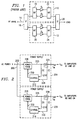
- FIGURE 1 is a block diagram of a RF power amplifier that is designed to operate in the frequency range of 225 to 400 MHz. It includes a pair of 90° hybrid coupled amplifiers, 10 and 12.
- the RF signal to be transmitted is received on line 14 by hybrid coupler 16, which in turn provides the signal to each of hybrid amplifiers 10 and 12.
- hybrid coupler 16 which in turn provides the signal to each of hybrid amplifiers 10 and 12.
- second hybrid couplers 18 and 20, respectively split the RF signals again such that the RF signals supplied to transistors Q1 and Q3 are in-phase and the RF signals supplied to transistors Q2 and Q4 are in-phase, but 90° out of phase with the RF signals supplied to transistors Q1 and Q3.
- Hybrid coupler 26 combines the outputs of the two hybrid couplers to form an amplified RF signal that is coupled to the load.
- the RF power amplifier of FIGURE 1 is an example of a type of power amplifier utilized in connection with the invention to be subsequently described. As will be apparent, the invention may also be used with an amplifier having a single solid state device, as well as with one having multiple, parallel stages.
- FIGURE 2 a block diagram of an adaptive power supply in accordance with the teachings of the invention, for use with the RF power amplifier described in Figure 1 is depicted. It comprises two power supplies 204 and 206.
- Power supply 204 provides an output voltage coupled to transistors Q1 and Q3 operating in phase
- power supply 206 provides an output voltage coupled to transistors Q2 and Q4 operating in phase.
- Alternating current (AC) power at 400 Hz is supplied on lines 202 to each of the power supplies 204 and 206.
- the power stages are switching power converters.
- control circuits 212 and 214 Associated with each power stage 208 and 210 are control circuits 212 and 214 respectively.
- a control circuit forms part of a dynamic control loop that controls the voltage (Vdc) of the output of the power stage associated with the particular control circuit.
- the control circuits 212 and 214 sample Vdc of power stages 208 and 210 by lines 216 and 218, respectively.
- the control circuits 212 and 214 also form part of current control loops that sample the dc load currents (Idc) of the output power signals on lines 223 and 225 using current sampling devices 224 and 226, respectively.
- the current control loops provide a current feedback signal representative of Idc to control circuits 212 and 214 by connecting lines 228 and 230, respectively.
- control circuits 212 and 214 In response to the feedback voltage on lines 216 and 218, and the current feedback on line 228 and 230, control circuits 212 and 214 generate control signals such that Vdc of the output of the respective power stages 208 and 210 follow a predetermined voltage and current characteristic.
- dual power stages are intended to be illustrative of only one possible application of an adaptive power supply in accordance with the present invention.
- a single stage power supply is required for a power amplifier with transistors that are not operating in quadrature phase.
- the single power stage may supply the Vdc signal to one or a plurality of parallel transistors operating in phase with one another, the number of transistors being limited only by ability of the power stage to supply the required power.
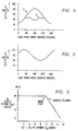
- each control circuit controls the output voltage level of a power stage in accordance with the voltage and current characteristic shown by the graph.
- the voltage feedback loop of each circuit maintains a steady voltage at 28 volts for Idc between 0 and 10 amps.
- the current feedback loop "foldbacks" Vdc as Idc increases the break point.
- the graph demonstrates a linear relationship between Vdc and Idc during the foldback that maintains power supplied to the RF power amplifier at a fixed wattage level.
- the RF power amplifier shown in FIGURE 1 with the adaptive power supply of the present invention generating this voltage and current characteristic, has been shown to maintain a 250 watt power output into a 3 to 1 VSWR load.
- the Vdc and the Idc at breakpoint and the slope of the foldback are chosen for a particular application depending on the particular RF power amplifier and the expected VSWR load condition on the output of the power amplifier.
- the foldback characteristic is adaptable to any VSWR condition.
- the voltage and current characteristic need not necessarily be linear. Although it is shown to be piece-wise linear, the voltage and current characteristic may be customized for the particular application with a non-linear function or programmed with an empirically determined voltage and current relationship that avoids the deleterious affects of excessive power dissipation while maintaining the desired power output.
- this waveform plot illustrates power dissipated by the transistor Q1 or Q3, of the power amplifier shown in Figure 1, versus a load phase under a 3 to 1 VSWR load.
- the curve designated “A” represents power dissipated by a transistor that is supplied by a non-adaptive power supply without the voltage foldback feature.
- the curve designated by “B” represents power dissipated by a transistor when the voltage to the transistor is supplied by the adaptive power supply operated according the present invention.
- the plot demonstrates a reduction in the amount of power dissipated by a transistor supplied by the adaptive power supply and relatively constant power dissipation for providing constant transistor efficiency.
- the waveform plot illustrates the RF power output of transistor Q1 or Q3 of the RF power amplifier depicted by Figure 1 with the RF power amplifier coupled to the adaptive power supply of the invention, versus the load phase.
- the load is a 3 to 1 VSWR load and the dual output of Q1 and Q3 equals 125 watts total.
- the plot shows an RF power output substantially identical to that of an RF power amplifier, with a non-adaptive power supply, thus, demonstrating that use of the adaptive power supply in accordance with the present invention does not reduce the forward power output of a RF power amplifier.
Landscapes
- Engineering & Computer Science (AREA)
- Power Engineering (AREA)
- Amplifiers (AREA)
Claims (3)
- Bloc d'alimentation (204) ayant un système de réaction dynamique pour contrôler indirectement la puissance tirée par un amplificateur de puissance adaptatif suivant le rapport d'ondes stationnaires (Q1, Q3) dans lequel le bloc d'alimentation comprend un étage de puissance (208) pour générer un signal de puissance ayant un niveau de tension adjustable, le signal de puissance est appliqué à l'amplificateur de puissance adaptatif suivant le rapport d'ondes stationnaires (Q1, Q3), un asservisseur (212) ayant une première entrée et une seconde entrée et un capteur (224) réagit au niveau de courant de charge fourni par l'étage de puissance (208) à l'amplificateur de puissance adaptatif suivant le rapport d'ondes stationnaires (Q1, Q3), caractérisé par : l'asservisseur (212) ayant la première entrée reliée à l'étage de puissance (208) et recevant le niveau de tension du signal de puissance, la seconde entrée de l'asservisseur (212) reliée au capteur (224) pour échantillonner les courants de charge de l'amplificateur de puissance adaptatif suivant le rapport d'ondes stationnaires (Q1, Q3), l'asservisseur (212) comprenant un circuit de commande qui réagit aux courants de charge échantillonnés et au niveau de tension du signal de puissance pour générer un signal de réglage de réaction couplé à l'étage de puissance (208) pour maintenir un niveau de tension essentiellement constant pour un niveau de courant de charge au-dessous d'un niveau de courant de seuil présélectionné et ensuite rebaisser le niveau de tension du signal de puissance pour diminuer en proportion à une augmentation du niveau de courant de charge.
- Bloc d'alimentation selon la revendication 1, caractérisé de plus par l'asservisseur (212) comprenant des moyens pour générer un signal de réaction de tension représentatif du niveau de tension sortie palpé du signal de puissance.
- Bloc d'alimentation selon la revendication 2, caractérisé de plus par l'asservisseur (212) comprenant des moyens pour générer un signal de réaction de courant représentatif du niveau de courant de sortie palpé du signal de puissance.
Applications Claiming Priority (2)
| Application Number | Priority Date | Filing Date | Title |
|---|---|---|---|
| US07/527,777 US5081425A (en) | 1990-05-24 | 1990-05-24 | Vswr adaptive power amplifier system |
| US527777 | 2000-03-17 |
Publications (3)
| Publication Number | Publication Date |
|---|---|
| EP0458071A1 EP0458071A1 (fr) | 1991-11-27 |
| EP0458071B1 EP0458071B1 (fr) | 1996-01-03 |
| EP0458071B2 true EP0458071B2 (fr) | 2000-03-29 |
Family
ID=24102879
Family Applications (1)
| Application Number | Title | Priority Date | Filing Date |
|---|---|---|---|
| EP91106405A Expired - Lifetime EP0458071B2 (fr) | 1990-05-24 | 1991-04-20 | Système amplificateur de puissance adaptatif suivant le taux d'onde stationnaire |
Country Status (8)
| Country | Link |
|---|---|
| US (1) | US5081425A (fr) |
| EP (1) | EP0458071B2 (fr) |
| DE (1) | DE69115987T3 (fr) |
| DK (1) | DK0458071T3 (fr) |
| GR (1) | GR3018603T3 (fr) |
| IL (1) | IL98236A (fr) |
| NO (1) | NO179158C (fr) |
| TR (1) | TR25361A (fr) |
Families Citing this family (30)
| Publication number | Priority date | Publication date | Assignee | Title |
|---|---|---|---|---|
| US6148220A (en) | 1997-04-25 | 2000-11-14 | Triquint Semiconductor, Inc. | Battery life extending technique for mobile wireless applications |
| US6137366A (en) * | 1998-04-07 | 2000-10-24 | Maxim Integrated Products, Inc. | High VSWR mismatch output stage |
| US6097250A (en) * | 1999-04-22 | 2000-08-01 | Scientific-Atlanta, Inc. | Amplifier circuit |
| US6307364B1 (en) | 1999-08-27 | 2001-10-23 | Rf Micro Devices, Inc. | Power sensor for RF power amplifier |
| US6329809B1 (en) | 1999-08-27 | 2001-12-11 | Rf Micro Devices, Inc. | RF power amplifier output power sensor |
| DE19959406A1 (de) * | 1999-12-09 | 2001-06-13 | Rohde & Schwarz | 90 DEG -Leistungsteiler |
| US6265943B1 (en) | 2000-01-27 | 2001-07-24 | Rf Micro Devices, Inc. | Integrated RF power sensor that compensates for bias changes |
| US20030054780A1 (en) * | 2000-09-05 | 2003-03-20 | Hitachi, Ltd. | High frequency power amplifying circuit, and mobile communication apparatus using it |
| US6816012B2 (en) | 2000-10-10 | 2004-11-09 | California Institute Of Technology | Distributed circular geometry power amplifier architecture |
| US6856199B2 (en) | 2000-10-10 | 2005-02-15 | California Institute Of Technology | Reconfigurable distributed active transformers |
| GB0028689D0 (en) * | 2000-11-24 | 2001-01-10 | Qualcomm Uk Ltd | Amplifier circuit |
| US6683496B2 (en) | 2001-08-20 | 2004-01-27 | Harris Corporation | System and method for minimizing dissipation in RF power amplifiers |
| US6611169B2 (en) * | 2001-10-01 | 2003-08-26 | Gibson Guitar Corp. | Power supply regulation and protection circuit for audio power amplifier |
| TWI326967B (en) | 2002-03-11 | 2010-07-01 | California Inst Of Techn | Differential amplifier |
| US6624702B1 (en) | 2002-04-05 | 2003-09-23 | Rf Micro Devices, Inc. | Automatic Vcc control for optimum power amplifier efficiency |
| US6856200B1 (en) | 2002-09-19 | 2005-02-15 | Marvell International Ltd. | Protection circuit and method for RF power amplifiers in WLAN tranceivers |
| US20040072554A1 (en) * | 2002-10-15 | 2004-04-15 | Triquint Semiconductor, Inc. | Automatic-bias amplifier circuit |
| US20040070454A1 (en) * | 2002-10-15 | 2004-04-15 | Triquint Semiconductor, Inc. | Continuous bias circuit and method for an amplifier |
| US7010284B2 (en) * | 2002-11-06 | 2006-03-07 | Triquint Semiconductor, Inc. | Wireless communications device including power detector circuit coupled to sample signal at interior node of amplifier |
| US7177370B2 (en) * | 2003-12-17 | 2007-02-13 | Triquint Semiconductor, Inc. | Method and architecture for dual-mode linear and saturated power amplifier operation |
| JP2005191791A (ja) * | 2003-12-25 | 2005-07-14 | Matsushita Electric Ind Co Ltd | 電力増幅器の保護回路 |
| WO2005098880A2 (fr) * | 2004-03-31 | 2005-10-20 | Axiom Microdevices, Inc. | Techniques de commande de puissance dat |
| US7710204B2 (en) * | 2005-04-18 | 2010-05-04 | Freescale Semiconductor, Inc. | Adaptive protection circuit for a power amplifier |
| US7330070B2 (en) * | 2005-11-10 | 2008-02-12 | Nokia Corporation | Method and arrangement for optimizing efficiency of a power amplifier |
| US7590395B2 (en) * | 2006-07-27 | 2009-09-15 | Harris Corporation | Power management scheme for software-defined radios |
| US7733176B2 (en) | 2006-09-08 | 2010-06-08 | Infineon Technologies Ag | System and method for power amplifier output power control |
| US7486137B2 (en) | 2006-09-08 | 2009-02-03 | Axiom Microdevices, Inc. | System and method for power amplifier output power control |
| US7710197B2 (en) | 2007-07-11 | 2010-05-04 | Axiom Microdevices, Inc. | Low offset envelope detector and method of use |
| EP2953425B1 (fr) | 2014-06-03 | 2019-08-21 | Ampleon Netherlands B.V. | Appareil de chauffage à fréquence radio |
| US10720310B2 (en) | 2017-09-14 | 2020-07-21 | Cellencor, Inc. | High-power solid-state microwave generator for RF energy applications |
Family Cites Families (34)
| Publication number | Priority date | Publication date | Assignee | Title |
|---|---|---|---|---|
| NL270662A (fr) * | 1960-10-26 | |||
| US3239774A (en) * | 1961-06-20 | 1966-03-08 | Blonder Tongue Elect | Transistor power supply which minimizes distortion |
| US3263172A (en) * | 1963-06-20 | 1966-07-26 | Motorola Inc | Transistor transmitter output amplifier protection means |
| US3281697A (en) * | 1963-12-04 | 1966-10-25 | Motorola Inc | Transmitter output transistor burnout protection |
| US3323065A (en) * | 1964-05-11 | 1967-05-30 | Motorola Inc | Transistor protection circuit for radio transmitter |
| US3426290A (en) * | 1965-10-20 | 1969-02-04 | Honeywell Inc | Amplifier having series regulated voltage supply |
| US3423688A (en) * | 1965-11-09 | 1969-01-21 | Bell Telephone Labor Inc | Hybrid-coupled amplifier |
| US3428909A (en) * | 1965-12-30 | 1969-02-18 | Sylvania Electric Prod | Automatic control of drive for linear power amplifier |
| US3478275A (en) * | 1966-01-21 | 1969-11-11 | Dana Lab Inc | Amplifier system with power supply control for a balanced power |
| US3449680A (en) * | 1966-03-29 | 1969-06-10 | Motorola Inc | Transistor protection circuit |
| US3403357A (en) * | 1966-04-14 | 1968-09-24 | Hughes Aircraft Co | Switching apparatus for selectively coupling a predetermined number of microwave devices between an input and an output port |
| US3510790A (en) * | 1967-11-14 | 1970-05-05 | Motorola Inc | Semiconductor protection system |
| US3521179A (en) * | 1968-04-02 | 1970-07-21 | Weston Instruments Inc | Amplifier with source voltage control |
| US3668545A (en) * | 1969-11-03 | 1972-06-06 | Scott Inc H H | Apparatus for amplifier protection |
| US3671878A (en) * | 1970-04-27 | 1972-06-20 | Motorola Inc | Protection circuit for an amplifier |
| US3644832A (en) * | 1970-09-28 | 1972-02-22 | Gen Electric | Power control circuit |
| US3753138A (en) * | 1971-06-03 | 1973-08-14 | Ampex | Amplifier system with continuously variable supply |
| US3714601A (en) * | 1971-10-14 | 1973-01-30 | Us Navy | Variable direct current bias control circuit for linear operation of radio frequency power transistors |
| US3962648A (en) * | 1975-01-20 | 1976-06-08 | E-Systems, Inc. | Function generator |
| DE2519845C3 (de) * | 1975-05-03 | 1978-06-08 | Licentia Patent-Verwaltungs-Gmbh, 6000 Frankfurt | Schaltungsanordnung zur Zusammenführung von Hochfrequenzleistungsanteilen |
| US3996524A (en) * | 1975-11-05 | 1976-12-07 | Rca Corporation | Linear amplifier utilizing adaptive biasing |
| US4064464A (en) * | 1976-04-13 | 1977-12-20 | Westinghouse Electric Corporation | Amplitude stabilized power amplifier |
| US4146847A (en) * | 1976-11-05 | 1979-03-27 | Trio Kabushiki Kaisha | Power limiting circuitry for use with power amplifier |
| US4114108A (en) * | 1977-05-19 | 1978-09-12 | General Electric Company | Overdrive protection circuit |
| JPS5442967A (en) * | 1977-09-02 | 1979-04-05 | Fujitsu Ltd | Bias supply circuit |
| JPS5510208A (en) * | 1978-07-07 | 1980-01-24 | Hitachi Ltd | Aso protection circuit |
| US4320350A (en) * | 1979-11-29 | 1982-03-16 | Rockwell International Corporation | Sliding power supply for RF power amplifier |
| FR2482799A1 (fr) * | 1980-05-14 | 1981-11-20 | Lgt Lab Gen Telecomm | Dispositif de precorrection de produits de non linearite et systeme de transmission de signaux de television comportant de tel dispositif |
| US4380089A (en) * | 1980-06-16 | 1983-04-12 | Gte Products Corporation | Battery-powered transmitter including current control circuit |
| JPS5768911A (en) * | 1980-10-16 | 1982-04-27 | Victor Co Of Japan Ltd | Complementary type emitter follower circuit |
| US4442407A (en) * | 1982-06-11 | 1984-04-10 | The United States Of America As Represented By The Secretary Of The Army | Two loop automatic level control for power amplifier |
| US4531173A (en) * | 1983-11-02 | 1985-07-23 | Motorola, Inc. | Protective power foldback circuit for a power semiconductor |
| US4547746A (en) * | 1984-04-09 | 1985-10-15 | Rockwell International Corporation | VSWR Tolerant linear power amplifier |
| US4656434A (en) * | 1986-02-03 | 1987-04-07 | Raytheon Company | RF power amplifier with load mismatch compensation |
-
1990
- 1990-05-24 US US07/527,777 patent/US5081425A/en not_active Expired - Lifetime
-
1991
- 1991-04-20 EP EP91106405A patent/EP0458071B2/fr not_active Expired - Lifetime
- 1991-04-20 DE DE69115987T patent/DE69115987T3/de not_active Expired - Lifetime
- 1991-04-20 DK DK91106405.3T patent/DK0458071T3/da active
- 1991-05-14 TR TR91/0531A patent/TR25361A/xx unknown
- 1991-05-23 IL IL9823691A patent/IL98236A/en not_active IP Right Cessation
- 1991-05-23 NO NO911990A patent/NO179158C/no unknown
-
1996
- 1996-01-04 GR GR950403716T patent/GR3018603T3/el unknown
Also Published As
| Publication number | Publication date |
|---|---|
| IL98236A0 (en) | 1992-06-21 |
| NO179158C (no) | 1996-08-14 |
| EP0458071B1 (fr) | 1996-01-03 |
| DE69115987T2 (de) | 1996-09-05 |
| US5081425A (en) | 1992-01-14 |
| DE69115987T3 (de) | 2000-07-27 |
| IL98236A (en) | 1994-07-31 |
| EP0458071A1 (fr) | 1991-11-27 |
| NO911990L (no) | 1991-11-25 |
| DK0458071T3 (da) | 1996-02-19 |
| NO179158B (no) | 1996-05-06 |
| DE69115987D1 (de) | 1996-02-15 |
| NO911990D0 (no) | 1991-05-23 |
| GR3018603T3 (en) | 1996-04-30 |
| TR25361A (tr) | 1993-03-01 |
Similar Documents
| Publication | Publication Date | Title |
|---|---|---|
| EP0458071B2 (fr) | Système amplificateur de puissance adaptatif suivant le taux d'onde stationnaire | |
| EP2089981B1 (fr) | Circuit de commutation d'antenne pour trajet de transmission sans perte | |
| KR100318788B1 (ko) | 안정성증가를위한rf플라즈마전력공급기결합방법 | |
| US6301486B1 (en) | Radio telephone apparatus | |
| US5561395A (en) | Method and apparatus for self-adjusting a multistage radio frequency power amplifier | |
| JP3568994B2 (ja) | 電力レベル制御用の方向性検波装置 | |
| US20040075504A1 (en) | Method and arrangement for detecting load mismatch, and a radio device utilizing the same | |
| US5678209A (en) | Transmit power level detection circuit with enhanced gain characteristics | |
| EP1248363B1 (fr) | Commande pour un amplificateur de puissance haute fréquence présentant une sensibilité réduite à la longueur du cable | |
| CN115242200B (zh) | 一种c波段射频信号功率放大装置和方法 | |
| CN221202513U (zh) | 一种射频功放过输入保护的装置 | |
| EP1179222A1 (fr) | Amplificateur de puissance radioelectrique avec retour du port d'isolation d'un coupleur hybride | |
| WO2024182926A1 (fr) | Circuit de protection de désadaptation d'amplificateur de puissance et dispositif électronique | |
| EP1400011B1 (fr) | Circuit de commande d'emetteur | |
| US3458826A (en) | Automatic power controls for amplifiers | |
| JPH04291167A (ja) | 高周波電力検出用検波器 | |
| KR940001233Y1 (ko) | 고주파 전력증폭기 보호회로 | |
| WO2000026680A1 (fr) | Dispositif de gestion de la consommation pour systemes electriques | |
| JP2002009641A (ja) | デバイス保護装置 | |
| JPH11233296A (ja) | 加速器rfシステム | |
| JPS6214760Y2 (fr) | ||
| JPS6041822A (ja) | 送信出力電力制御装置 | |
| JP2000341142A (ja) | 自動送信出力制御装置 | |
| JPH03277006A (ja) | 高周波電力出力制御方法 | |
| JPH08287768A (ja) | 高周波信号用遮断器 |
Legal Events
| Date | Code | Title | Description |
|---|---|---|---|
| PUAI | Public reference made under article 153(3) epc to a published international application that has entered the european phase |
Free format text: ORIGINAL CODE: 0009012 |
|
| AK | Designated contracting states |
Kind code of ref document: A1 Designated state(s): BE CH DE DK GB GR IT LI NL SE |
|
| 17P | Request for examination filed |
Effective date: 19920428 |
|
| 17Q | First examination report despatched |
Effective date: 19941010 |
|
| GRAA | (expected) grant |
Free format text: ORIGINAL CODE: 0009210 |
|
| AK | Designated contracting states |
Kind code of ref document: B1 Designated state(s): BE CH DE DK GB GR IT LI NL SE |
|
| PG25 | Lapsed in a contracting state [announced via postgrant information from national office to epo] |
Ref country code: GR Free format text: LAPSE BECAUSE OF FAILURE TO SUBMIT A TRANSLATION OF THE DESCRIPTION OR TO PAY THE FEE WITHIN THE PRESCRIBED TIME-LIMIT Effective date: 19960103 Ref country code: LI Effective date: 19960103 Ref country code: NL Free format text: LAPSE BECAUSE OF FAILURE TO SUBMIT A TRANSLATION OF THE DESCRIPTION OR TO PAY THE FEE WITHIN THE PRESCRIBED TIME-LIMIT Effective date: 19960103 Ref country code: CH Effective date: 19960103 Ref country code: BE Effective date: 19960103 |
|
| REF | Corresponds to: |
Ref document number: 69115987 Country of ref document: DE Date of ref document: 19960215 |
|
| REG | Reference to a national code |
Ref country code: DK Ref legal event code: T3 |
|
| ITF | It: translation for a ep patent filed | ||
| REG | Reference to a national code |
Ref country code: GR Ref legal event code: FG4A Free format text: 3018603 |
|
| PG25 | Lapsed in a contracting state [announced via postgrant information from national office to epo] |
Ref country code: SE Effective date: 19960403 |
|
| PG25 | Lapsed in a contracting state [announced via postgrant information from national office to epo] |
Ref country code: DK Effective date: 19960420 |
|
| REG | Reference to a national code |
Ref country code: DK Ref legal event code: EBP |
|
| NLV1 | Nl: lapsed or annulled due to failure to fulfill the requirements of art. 29p and 29m of the patents act | ||
| REG | Reference to a national code |
Ref country code: CH Ref legal event code: PL |
|
| PLBQ | Unpublished change to opponent data |
Free format text: ORIGINAL CODE: EPIDOS OPPO |
|
| PLBI | Opposition filed |
Free format text: ORIGINAL CODE: 0009260 |
|
| 26 | Opposition filed |
Opponent name: DAIMLER-BENZ AEROSPACE AG SENSORSYSTEME Effective date: 19960730 |
|
| PLBQ | Unpublished change to opponent data |
Free format text: ORIGINAL CODE: EPIDOS OPPO |
|
| PLAB | Opposition data, opponent's data or that of the opponent's representative modified |
Free format text: ORIGINAL CODE: 0009299OPPO |
|
| PLBQ | Unpublished change to opponent data |
Free format text: ORIGINAL CODE: EPIDOS OPPO |
|
| PLBF | Reply of patent proprietor to notice(s) of opposition |
Free format text: ORIGINAL CODE: EPIDOS OBSO |
|
| PLAB | Opposition data, opponent's data or that of the opponent's representative modified |
Free format text: ORIGINAL CODE: 0009299OPPO |
|
| R26 | Opposition filed (corrected) |
Opponent name: DAIMLER-BENZ AEROSPACE AG SENSORSYSTEME Effective date: 19960730 |
|
| REG | Reference to a national code |
Ref country code: GR Ref legal event code: MM2A Free format text: 3018603 |
|
| R26 | Opposition filed (corrected) |
Opponent name: DAIMLER-BENZ AEROSPACE AG Effective date: 19960730 |
|
| PLBF | Reply of patent proprietor to notice(s) of opposition |
Free format text: ORIGINAL CODE: EPIDOS OBSO |
|
| PLBF | Reply of patent proprietor to notice(s) of opposition |
Free format text: ORIGINAL CODE: EPIDOS OBSO |
|
| PLAW | Interlocutory decision in opposition |
Free format text: ORIGINAL CODE: EPIDOS IDOP |
|
| PLAW | Interlocutory decision in opposition |
Free format text: ORIGINAL CODE: EPIDOS IDOP |
|
| PUAH | Patent maintained in amended form |
Free format text: ORIGINAL CODE: 0009272 |
|
| STAA | Information on the status of an ep patent application or granted ep patent |
Free format text: STATUS: PATENT MAINTAINED AS AMENDED |
|
| ITF | It: translation for a ep patent filed | ||
| 27A | Patent maintained in amended form |
Effective date: 20000329 |
|
| AK | Designated contracting states |
Kind code of ref document: B2 Designated state(s): BE CH DE DK GB GR IT LI NL SE |
|
| EN | Fr: translation not filed | ||
| REG | Reference to a national code |
Ref country code: GB Ref legal event code: IF02 |
|
| PLAB | Opposition data, opponent's data or that of the opponent's representative modified |
Free format text: ORIGINAL CODE: 0009299OPPO |
|
| PGFP | Annual fee paid to national office [announced via postgrant information from national office to epo] |
Ref country code: GB Payment date: 20100325 Year of fee payment: 20 |
|
| PGFP | Annual fee paid to national office [announced via postgrant information from national office to epo] |
Ref country code: IT Payment date: 20100421 Year of fee payment: 20 Ref country code: DE Payment date: 20100430 Year of fee payment: 20 |
|
| REG | Reference to a national code |
Ref country code: DE Ref legal event code: R071 Ref document number: 69115987 Country of ref document: DE |
|
| REG | Reference to a national code |
Ref country code: GB Ref legal event code: PE20 Expiry date: 20110419 |
|
| PG25 | Lapsed in a contracting state [announced via postgrant information from national office to epo] |
Ref country code: GB Free format text: LAPSE BECAUSE OF EXPIRATION OF PROTECTION Effective date: 20110419 |
|
| PG25 | Lapsed in a contracting state [announced via postgrant information from national office to epo] |
Ref country code: DE Free format text: LAPSE BECAUSE OF EXPIRATION OF PROTECTION Effective date: 20110420 |