EP0457625A2 - Staubdichte Schicht für Wellenleiter und Verfahren zu seiner Herstellung - Google Patents
Staubdichte Schicht für Wellenleiter und Verfahren zu seiner Herstellung Download PDFInfo
- Publication number
- EP0457625A2 EP0457625A2 EP91304519A EP91304519A EP0457625A2 EP 0457625 A2 EP0457625 A2 EP 0457625A2 EP 91304519 A EP91304519 A EP 91304519A EP 91304519 A EP91304519 A EP 91304519A EP 0457625 A2 EP0457625 A2 EP 0457625A2
- Authority
- EP
- European Patent Office
- Prior art keywords
- film
- dustproofing
- region
- electromagnetic wave
- waveguide
- Prior art date
- Legal status (The legal status is an assumption and is not a legal conclusion. Google has not performed a legal analysis and makes no representation as to the accuracy of the status listed.)
- Withdrawn
Links
Images


Classifications
-
- H—ELECTRICITY
- H01—ELECTRIC ELEMENTS
- H01P—WAVEGUIDES; RESONATORS, LINES, OR OTHER DEVICES OF THE WAVEGUIDE TYPE
- H01P11/00—Apparatus or processes specially adapted for manufacturing waveguides or resonators, lines, or other devices of the waveguide type
-
- H—ELECTRICITY
- H01—ELECTRIC ELEMENTS
- H01P—WAVEGUIDES; RESONATORS, LINES, OR OTHER DEVICES OF THE WAVEGUIDE TYPE
- H01P1/00—Auxiliary devices
- H01P1/30—Auxiliary devices for compensation of, or protection against, temperature or moisture effects ; for improving power handling capability
Definitions
- This invention relates to a dustproofing film for a waveguide to be used in the formation of a primary radiation device of a parabolic antenna and to a method for the production thereof.
- the wave from an artificial satellite is converged by a reflecting mirror of a parabolic antenna 1 installed outdoors and the converged wave is received by a primary radiation device 2 as illustrated in Fig. 11. Then, the received signal is processed by a tuner installed indoors and the resultant reproduced image is displayed on a television receiver.
- the primary radiation device 2 of the parabolic antenna 1, as illustrated in Fig. 12, comprises a flared horn 3 serving as an entrance for the wave converged by the reflecting mirror, a waveguide 4 serving as a transmitting path for electromagnetic wave energy, and a low noise block converter (LNB) 5 serving as a receiver connected to the trailing end of the waveguide 4.
- the LNB 5 is a waveguide of one kind.
- the primary radiation device 2 illustrated in Fig. 12 is portrayed as having inside the waveguide 4 a polarizer 6.
- the term "polarizer" as used herein means a device for discriminating a cross polarized electromagnetic radiation in the radio communication system.
- two perpendicularly cross polarized electromagnetic radiations (a vertically polarized electromagnetic radiation and a horizontally polarized electromagnetic radiation in the linear polarized electromagnetic radiations) are simultaneously utilized for the purpose of augmenting the capacity for communication and, at the same time, avoiding interference with radio channels.
- a coil 7 of the polarizer 6 is operated to induce Faraday rotation of the received electromagnetic wave and effect discrimination between the vertically polarized electromagnetic radiation and the horizontally polarized electromagnetic radiation in the cross polarized electromagnetic radiations.
- the component parts which are incorporated in the primary radiation device 2 as described above are individually manufactured, stored, and managed and are combined to assemble the primary radiation device at the site of installation.
- the waveguide 4 and the LNB 5 as manufactured are stored in a warehouse, transported in the process of commercial distribution, or installed and put to service, fine dust steals its way into the waveguide 4 and the LNB 5.
- the dust enters their interiors, the wave passing their internal transmission paths collides against the dust and gets reflected randomly and succumbs to the drawback of the so-called insertion loss by being seriously attenuated or absorbed.
- a dustproofing film 9 formed of a film 9a such as of polyimide resin having an adhesive agent 8 applied across the whole of one surface thereof is fixedly attached to an opening 4a side of the waveguide 4 as illustrated in Fig. 13 so as to prevent the dust from entering the interior.
- a peel paper (not shown) is kept attached to the adhesive agent 8 side of the dustproofing film 9 until the dustproofing film 9 is put to use.
- the adhesive agent 8 is applied across the whole of one side of the dustproofing film 9, the electromagnetic wave which penetrates the dustproofing film 9 and reaches the interiors of the waveguide 4 and the LNB 5 entails the drawback of insertion loss, though in a different sense from the aforementioned insertion loss, by being reflected, attenuated, or absorbed by the adhesive agent 8.
- the conventional dustproofing film 9 consequently degrades the gain of the waveguide and exerts an adverse effect on the ability of the parabolic antenna 1 to receive the electromagnetic wave, a fact which forms a fatal drawback for receiving devices of this class used in satellite broadcasting. This statement holds good with other waveguide-containing systems than those for use in satellite broadcasting.
- An object of this invention is to provide a dustproofing film for a waveguide free from the drawbacks of the prior art mentioned above and which does not induce the phenomenon of insertion loss,and a method for the production thereof.
- the dustproofing film of this invention is characterized by having an adhesive agent applied to a peripheral area thereof and having formed in the area thereof surrounded by the peripheral area a region completely free of adhering substance and permeable to the electromagnetic wave.
- the dustproofing film of this invention has no adhesive agent applied to the region thereof intended for passage of the electromagnetic wave. It does not, therefore entail the insertion loss due to an adhesive agent as encountered heretofore.
- the method for the production of the dustproofing film of this invention comprises cutting a prescribed shape from a double-faced adhesive tape which has a peel paper on each side, removing a peel paper from one surface of the part of the adhesive tape remaining after the removal of the shape mentioned above, applying the adhesive side of the remaining adhesive tape to a film formed of a synthetic resin such as polyimide thereby forming a sheet material having formed in the part of the prescribed shape cut out of the double-faced adhesive tape a region covered with neither the adhesive agent nor the peel paper and consequently allowed to pass the electromagnetic wave, and cutting a prescribed shape from the sheet material around the periphery of the region used for passage of the electromagnetic wave thereby forming around the periphery of the region for passage of the electromagnetic wave a peripheral region having a peel paper attached thereto through the medium of the adhesive agent.
- a synthetic resin such as polyimide
- the dustproofing film of this invention by cutting the prescribed shape from the double-faced adhesive tape with two peel papers, removing a peel paper from one side of the adhesive tape, and applying the adhesive side of this adhesive tape to a film, there is obtained the sheet material which has formed in the part removed in the prescribed shape the region containing the film alone and consequently allowing passage of the electromagnetic wave. Then, by cutting the entire sheet material around the periphery of the permeable region, thereby forming around the periphery of the region for passage of the electromagnetic wave a peripheral region having a peel paper attached thereto through the medium of the adhesive agent, there is completed the dustproofing film.
- the dustproofing film can be produced simply by cutting and removing the sheet material of a three-layer construction. This method is extremely simple as compared with the method which comprises attaching an adhesive agent and a peel paper exclusively to part of the peripheral region.
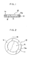
- Fig. 1 is a longitudinal cross section of a dustproofing film as one embodiment of the present invention.
- Fig. 2 is a plan view of the dustproofing film of Fig. 1.
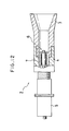
- Fig. 3 is a longitudinal cross section illustrating the state in which the dustproofing film is applied fast to a waveguide.
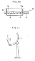
- Fig. 5, Fig. 6, Fig. 7, Fig. 8, Fig. 9, and Fig. 10 are longitudinal cross sections illustrating serially-a process for the production of a dustproofing film according to the present invention.
- Fig. 11 is a schematic side elevation of a parabolic antenna.
- Fig. 12 is a partially sectioned side elevation of a primary radiation device.
- Fig. 13 is a longitudinal cross section illustrating the state in which the conventional dustproofing film is applied to a waveguide.
- Fig. 1 and Fig. 2 illustrate a dustproofing film 10 as one embodiment of this invention.
- a film 11 of polyimide resin produced by DuPont and Company and marketed under trademark designation of "Capton” is prepared.
- a peripheral edge region 14 is formed by applying a double-faced adhesive tape 20 produced by Sony Chemical Co., Ltd. and marketed under product code of "T4100" fast around the periphery of the film 11.
- the double-faced tape 20, as illustrated in Fig. 5 has peel papers 13a and 13b attached to the opposite surfaces of an adhesive agent 12.
- the dustproofing film 10 has formed in the area surrounded by the peripheral region 14 a region 15 not covered at all with the adhesive agent 12 and consequently allowing the electromagnetic wave to pass.
- a handling piece 16 may be disposed in part of the peripheral edge of the dustproofing film of the peel paper 13a as indicated by a chain line in Fig. 2 so that when a person is about to apply the dustproofing film to a given surface, he is able to grip the dustproofing film by this handling piece without smearing the region 15 for passage of the electromagnetic wave with the dirt from his hand and then may peel the peel paper 13a and position the dustproofing film 10 as a whole with ease.
- This handling piece 16 may be formed on the film 11 side.
- the dustproofing film 10 which is constructed as described above is produced by the following procedure. First, the adhesion agent 12 is applied throughout to one surface of the peel paper 13b as illustrated in Fig. 4. Subsequently, the peel paper 13a is attached to the adhesive agent 12 as illustrated in Fig. 5, to form the double-faced tape 20 of the form of a three-layer sheet. Then, a cylindrical punching blade 18 is prepared and passed through the double-faced tape 20 to cut out a circle (in the state shown in Fig. 7) as illustrated in Fig. 6. Subsequently, the peel paper 13b on the lower surface side is removed as illustrated in Fig. 8 and the remaining part of the tape 20 is applied fast to the film 11 of the form of a sheet as illustrated in Fig.
- the dustproofing film 10 is produced which has the peel paper 13a attached thereto through the medium of the adhesive agent 12 around the periphery of the region 15 for passage of the electromagnetic wave.
- the dustproofing film 10 produced as described above is put to use by having the peel paper 13a removed and then having the exposed surface of the dustproofing film 10 applied fast to the opening 4a side end face of the waveguide 4 through the medium of the adhesive agent 12 in the peripheral region 14 as illustrated in Fig. 3, for example.
- the region 15 for passage of the electromagnetic wave which is not covered at all with the adhesive agent 12 should be of a size identical to or slightly larger than the size of the opening 4a. This is because the adhesive agent 12 would be exposed on the inner surface side of the waveguide 4 and, similarly to the conventional countertype, would cause the phenomenon of insertion loss of the electromagnetic wave being transmitted inside the waveguide 4 if the aforementioned region 15 had a smaller size than the opening 4a.
- the handling piece 16 is available for the handling of the dustproofing film 10.
- the person gripping the dustproofing film 10 by the handling piece 16 is allowed to position the dustproofing film 10 relative to the waveguide 4.
- the provision of this handling piece 16 therefore, enables the application of the dustproofing film to a given surface to be carried out accurately, quickly, and easily.
- another method conceivable for the fast attachment of the film 11 would comprise applying the adhesive agent 12 to the opening 4a side end face and thereafter attaching the film all by itself to the adhesive agent.
- This method is not adoptable because it has the disadvantage that the applied layer of the adhesive agent 12 lacks uniformity of thickness and the applied adhesive agent 12 protrudes into the region 15 for passage of the electromagnetic wave and entails the conventional drawback.
- the following table shows the results of an experiment conducted by the present applicant to confirm the effect of this invention.
- a comparative sample obtained by preparing a waveguide 4 of a zinc alloy measuring 21 mm in inside diameter and 25 mm in outside diameter and applying the conventional dustproofing film 9 illustrated in Fig. 13 to the opening 4a side end face of the waveguide 4 and a sample of this invention obtained by similarly applying the dustproofing film 10 of this invention illustrated in Fig. 3 to the sample waveguide 4 as mentioned above were used.
- the two films were both made of Capton film 25 ⁇ m in thickness (produced by DuPont and Company) and the adhesive agents were both the product (T4100) of Sony Chemical Co., Ltd. applied in a thickness of 45 ⁇ m.
- the experiment consisted in projecting an electromagnetic wave of a frequency of 10.95 to 12.75 GHz through the dustproofing films 9 and 10, measuring the amounts of the electromagnetic wave which had permeated through the films, finding their differences, and determining the amounts of reflection as reflection loss and the amounts of absorption.
- the numerals indicated represent average values of the results of five measurements.
- the term "reflection loss” used herein means the sum of the amount reflected and the amount absorbed and the acronym “VSWR”used herein means the reflection loss obtained of the LNB.
- the waveguide comes in various types such as a circular waveguide, a square waveguide, and a ridge waveguide.
- the dustproofing film of this invention can be applied equally effectively to all of these types.
- the shape and the size of the dustproofing film are altered so as to suit the shape and the size of the particular kind of waveguide to be selected.
- a resinous material as Teflon may be used instead of the polyimide resin.
- the dustproofing film of this invention allows both the reflected and absorbed amounts of electromagnetic wave to be decreased because it is not covered at all by the adhesive agent in the region for passage of the electromagnetic wave as described above. It is, therefore, capable of amply lowering the reflection loss of the electromagnetic wave and notably improving the performances of devices for satellite broadcasting.
- the method of production according to this invention allows the dustproofing film to be produced simply by cutting the prescribed shape from the sheet material of a three-layer construction.
- the dustproofing film therefore, can be produced very accurately, rapidly, and easily.
Landscapes
- Engineering & Computer Science (AREA)
- Manufacturing & Machinery (AREA)
- Shielding Devices Or Components To Electric Or Magnetic Fields (AREA)
- Laminated Bodies (AREA)
- Waveguide Connection Structure (AREA)
- Non-Reversible Transmitting Devices (AREA)
- Details Of Aerials (AREA)
Applications Claiming Priority (2)
| Application Number | Priority Date | Filing Date | Title |
|---|---|---|---|
| JP129936/90 | 1990-05-18 | ||
| JP2129936A JPH0425203A (ja) | 1990-05-18 | 1990-05-18 | 導波管の防塵用フィルム及びその製造方法 |
Publications (2)
| Publication Number | Publication Date |
|---|---|
| EP0457625A2 true EP0457625A2 (de) | 1991-11-21 |
| EP0457625A3 EP0457625A3 (en) | 1992-08-12 |
Family
ID=15022096
Family Applications (1)
| Application Number | Title | Priority Date | Filing Date |
|---|---|---|---|
| EP19910304519 Withdrawn EP0457625A3 (en) | 1990-05-18 | 1991-05-20 | Dustproofing film for waveguide and method for production thereof |
Country Status (4)
| Country | Link |
|---|---|
| EP (1) | EP0457625A3 (de) |
| JP (1) | JPH0425203A (de) |
| KR (1) | KR940002991B1 (de) |
| TW (1) | TW200607B (de) |
Families Citing this family (2)
| Publication number | Priority date | Publication date | Assignee | Title |
|---|---|---|---|---|
| JP2009055490A (ja) * | 2007-08-29 | 2009-03-12 | Rohm Co Ltd | マイクロホン装置 |
| JP5306255B2 (ja) * | 2010-02-17 | 2013-10-02 | 三菱電機株式会社 | アンテナ放射素子及びこれを備えた平面アンテナ |
Family Cites Families (2)
| Publication number | Priority date | Publication date | Assignee | Title |
|---|---|---|---|---|
| US3201296A (en) * | 1959-04-09 | 1965-08-17 | Timothy J Kilduff | Method of making a waveguide window |
| NL7009767A (de) * | 1970-07-02 | 1972-01-04 |
-
1990
- 1990-05-18 JP JP2129936A patent/JPH0425203A/ja active Pending
-
1991
- 1991-05-15 KR KR1019910007847A patent/KR940002991B1/ko not_active Expired - Fee Related
- 1991-05-17 TW TW080103816A patent/TW200607B/zh active
- 1991-05-20 EP EP19910304519 patent/EP0457625A3/en not_active Withdrawn
Also Published As
| Publication number | Publication date |
|---|---|
| KR910020963A (ko) | 1991-12-20 |
| TW200607B (de) | 1993-02-21 |
| KR940002991B1 (ko) | 1994-04-09 |
| JPH0425203A (ja) | 1992-01-29 |
| EP0457625A3 (en) | 1992-08-12 |
Similar Documents
| Publication | Publication Date | Title |
|---|---|---|
| US6014110A (en) | Antenna and method for receiving or transmitting radiation through a dielectric material | |
| US5400043A (en) | Absorptive/transmissive radome | |
| DE69013839T2 (de) | Zwei dielektrische Anpassungsschichten aufweisende Struktur für Radome und Linsen für grosse Einfallswinkel. | |
| DE69812640T2 (de) | Radar-prüfsystem für fahrzeugskollisionsvermeidungsradar | |
| US20110267252A1 (en) | Non-Cutoff Frequency Selective Surface Ground Plane Antenna Assembly | |
| US5784021A (en) | Noiseless radar detector | |
| US9086476B1 (en) | Method and apparatus for rejecting intermodulation products | |
| CA2250083A1 (en) | Satellite broadcast system receiver | |
| US7420500B2 (en) | Electromagnetic radiation absorber | |
| WO1989010569A1 (en) | Method and apparatus for determining earth station parameters, such as rain margin, with attenuation pads | |
| EP0457625A2 (de) | Staubdichte Schicht für Wellenleiter und Verfahren zu seiner Herstellung | |
| EP0829737A2 (de) | Antireflexionsbehandlung von optischen Elementen | |
| Chu | Microwave depolarization of an earth‐space path | |
| US4748449A (en) | RF absorbing ablating apparatus | |
| DE3644891A1 (de) | Empfaenger fuer mikrowellen und millimeterwellen | |
| CA1263180A (en) | Linearly polarized grid reflector antenna systems with improved cross-polarization performance | |
| US6052094A (en) | Antenna system for millimeter wave length communication systems | |
| Ando et al. | AK/C/S bands satellite antenna with frequency selective surface | |
| EP0326746A3 (de) | Empfänger für RDS | |
| JPH0716121B2 (ja) | 分波器 | |
| US6144345A (en) | Variable attenuator for satellite signals | |
| Otoshi et al. | A portable Ku-band front-end test package for beam-waveguide antenna performance evaluation | |
| DE4028603A1 (de) | Dopplerradarsensor | |
| JPS61238108A (ja) | マイクロ波減衰器 | |
| CA1081845A (en) | Beam scanning |
Legal Events
| Date | Code | Title | Description |
|---|---|---|---|
| PUAI | Public reference made under article 153(3) epc to a published international application that has entered the european phase |
Free format text: ORIGINAL CODE: 0009012 |
|
| AK | Designated contracting states |
Kind code of ref document: A2 Designated state(s): CH DE ES FR GB IT LI |
|
| PUAL | Search report despatched |
Free format text: ORIGINAL CODE: 0009013 |
|
| AK | Designated contracting states |
Kind code of ref document: A3 Designated state(s): CH DE ES FR GB IT LI |
|
| 17P | Request for examination filed |
Effective date: 19920908 |
|
| 17Q | First examination report despatched |
Effective date: 19940727 |
|
| STAA | Information on the status of an ep patent application or granted ep patent |
Free format text: STATUS: THE APPLICATION IS DEEMED TO BE WITHDRAWN |
|
| 18D | Application deemed to be withdrawn |
Effective date: 19941207 |