EP0454902A2 - Circuit monolithique intégrÀ© avec diode à laser DFB, commutateur optique et connexions en guide d'onde - Google Patents
Circuit monolithique intégrÀ© avec diode à laser DFB, commutateur optique et connexions en guide d'onde Download PDFInfo
- Publication number
- EP0454902A2 EP0454902A2 EP90123353A EP90123353A EP0454902A2 EP 0454902 A2 EP0454902 A2 EP 0454902A2 EP 90123353 A EP90123353 A EP 90123353A EP 90123353 A EP90123353 A EP 90123353A EP 0454902 A2 EP0454902 A2 EP 0454902A2
- Authority
- EP
- European Patent Office
- Prior art keywords
- layer
- waveguide
- laser diode
- conductivity type
- grid
- Prior art date
- Legal status (The legal status is an assumption and is not a legal conclusion. Google has not performed a legal analysis and makes no representation as to the accuracy of the status listed.)
- Withdrawn
Links
Images
Classifications
-
- H—ELECTRICITY
- H01—ELECTRIC ELEMENTS
- H01S—DEVICES USING THE PROCESS OF LIGHT AMPLIFICATION BY STIMULATED EMISSION OF RADIATION [LASER] TO AMPLIFY OR GENERATE LIGHT; DEVICES USING STIMULATED EMISSION OF ELECTROMAGNETIC RADIATION IN WAVE RANGES OTHER THAN OPTICAL
- H01S5/00—Semiconductor lasers
- H01S5/02—Structural details or components not essential to laser action
- H01S5/026—Monolithically integrated components, e.g. waveguides, monitoring photo-detectors, drivers
-
- H—ELECTRICITY
- H01—ELECTRIC ELEMENTS
- H01S—DEVICES USING THE PROCESS OF LIGHT AMPLIFICATION BY STIMULATED EMISSION OF RADIATION [LASER] TO AMPLIFY OR GENERATE LIGHT; DEVICES USING STIMULATED EMISSION OF ELECTROMAGNETIC RADIATION IN WAVE RANGES OTHER THAN OPTICAL
- H01S5/00—Semiconductor lasers
- H01S5/10—Construction or shape of the optical resonator, e.g. extended or external cavity, coupled cavities, bent-guide, varying width, thickness or composition of the active region
- H01S5/12—Construction or shape of the optical resonator, e.g. extended or external cavity, coupled cavities, bent-guide, varying width, thickness or composition of the active region the resonator having a periodic structure, e.g. in distributed feedback [DFB] lasers
-
- H—ELECTRICITY
- H10—SEMICONDUCTOR DEVICES; ELECTRIC SOLID-STATE DEVICES NOT OTHERWISE PROVIDED FOR
- H10H—INORGANIC LIGHT-EMITTING SEMICONDUCTOR DEVICES HAVING POTENTIAL BARRIERS
- H10H29/00—Integrated devices, or assemblies of multiple devices, comprising at least one light-emitting semiconductor element covered by group H10H20/00
- H10H29/10—Integrated devices comprising at least one light-emitting semiconductor component covered by group H10H20/00
-
- H—ELECTRICITY
- H01—ELECTRIC ELEMENTS
- H01S—DEVICES USING THE PROCESS OF LIGHT AMPLIFICATION BY STIMULATED EMISSION OF RADIATION [LASER] TO AMPLIFY OR GENERATE LIGHT; DEVICES USING STIMULATED EMISSION OF ELECTROMAGNETIC RADIATION IN WAVE RANGES OTHER THAN OPTICAL
- H01S5/00—Semiconductor lasers
- H01S5/10—Construction or shape of the optical resonator, e.g. extended or external cavity, coupled cavities, bent-guide, varying width, thickness or composition of the active region
- H01S5/1028—Coupling to elements in the cavity, e.g. coupling to waveguides adjacent the active region, e.g. forward coupled [DFC] structures
- H01S5/1032—Coupling to elements comprising an optical axis that is not aligned with the optical axis of the active region
Definitions
- the present invention relates to the monolithic integration of a DFB laser diode with an optical switch and passive waveguide connections according to the features of the preamble of claim 1.
- Monolithically integrated circuits with laser diodes, optical switches and passive waveguides are regarded as key components of optical communication systems, since these circuits enable cost-effective implementations of signal distribution circuits and other system elements.
- the low-loss coupling of the laser diodes and the switches to passive waveguides is an essential prerequisite for the functionality of the integrated circuit. With the optical switch, this technical problem of coupling is relatively easy to solve.
- the design of high-performance optical switches corresponds to that of passive rib waveguides (RGHunsperger: "Integrated Optics: Theory and Technology, Springer Verlag, Berlin 1982, p. 43 ff.).
- the monolithic integration of high-performance laser diodes with such optical switches is the technical problem that Lasers with buried heterostructures are particularly suitable for monolithic integration.
- a DBR laser diode with a buried heterostructure and an optical switch in the form of a buried rib waveguide is described in the literature (F. Hernandez-Gil et. Al., Proc. CLEO 1989, Baltimore, pap. PD 17-1 / 2 ).
- the laser structure is arranged above the continuous passive waveguide.
- the lateral boundary of the laser strip and the concealment of the (buried) waveguide consist of semi-insulating semiconductor material, the production of which is not possible with all methods that are available in principle.
- the placement of the waveguide layer under the laser affects the properties of the laser, or forces a waveguide geometry and composition that degrades the optical properties of the waveguide of the switch.
- the object of the present invention is to provide a structure for a component in which at least one optical switch, which also has the shape of a ridge waveguide, and a DFB laser diode are monolithically integrated in passive waveguides in the form of ridge waveguides.
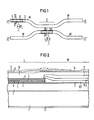
- Fig. 1 shows the laser switch waveguide structure according to the invention in a schematic plan view. Shown are the waveguides W with the light inputs port 1 P1 and port 2 P2 and the light outputs port 3 P3 and port 4 P4.
- the laser diode L with the laser current I L applied for operation is located at port 1 P1.
- the waveguide webs are approximated to one another up to a distance A.
- the switch is operated via a switch current I S.
- Fig. 1 shows an embodiment in a simplified top view without applied contact metallization. Different arrangements of laser diodes, in particular also several laser diodes and optical switches in ridge waveguides, are included in the construction according to the invention.
- Fig. 2 shows the transition from the laser diode to the waveguide in longitudinal section corresponding to the section shown in Fig. 1.
- the passive ridge waveguide which is shown on the right in FIG. 2, merges into the optical switch in almost unchanged form.
- This optical switch is not shown in FIG. 2 and is described below with reference to FIG. 4.
- the integrated circuit is located on a substrate 1 made of, for example, InP of a first conductivity type (for example n-type).
- Semiconductor layers are grown epitaxially on this substrate 1.
- the first layer grown on the substrate 1 is a buffer layer 2 of the same first conductivity type, for example also made of InP. If the overgrown surface of the substrate 1 is of sufficient quality, this buffer layer 2 can also be omitted.
- this buffer layer 2 is a thin etch stop layer 3 of a different composition from the composition of the buffer layer 2 (eg InGaAsP), but grown from the same first conductivity type.
- This etch stop layer 3 differs in its solubility in certain acids (for example HCl) from the buffer layer 2 or the substrate 1.
- the buffer layer 2 and the etch stop layer 3 are located in the entire area occupied by the functional elements of this circuit.
- a DFB grating is formed in the surface of this first grating layer 4. The grating period of this DFB grating corresponds to the wavelength of the light in the semiconductor material or an integer multiple thereof.
- a second grating layer 5 with a higher refractive index than that of the first grating layer 4 is grown on this first grating layer 4.
- This second grid layer 5 is e.g. InGaAsP and is also doped for electrical conductivity of the first conductivity type.
- This second lattice layer 5 compensates for the unevenness of the lattice, so that the second lattice layer 5 has a flat interface with an active layer 6 grown over it.
- This active layer 6 has the highest refractive index of all grown layers and is e.g. InGaAsP.
- the material composition of this active layer 6 determines the position of the amplification maximum of the laser in the spectrum of the laser.
- At least one anti-melt-back layer 7 has been grown on the active layer 6.
- This anti-melt-back layer 7 is doped for a second conductivity type opposite the first (in this exemplary embodiment p-type) and protects the active layer 6 from damaging influences during the manufacturing process.
- the further anti-melt-back layer 8 shown in FIG. 2 may have grown on this anti-melt-back layer 7.
- This further anti-melt-back layer 8 is e.g. B. InP and is doped for the second conductivity type. At the same time, it can serve to limit the current flow laterally to the area of the laser strip.
- This further anti-melt-back layer 8 can also be omitted.
- the laser layers i.e. the first grating layer 4, the second grating layer 5, the active layer 6 and the anti-melt-back layer 7 are delimited in the longitudinal and lateral directions by one or more waveguide layers 10.1, 10.2.
- a first waveguide layer 10.1, a second waveguide layer 10.2 and a first cladding layer 11 are present in the region of the waveguide W on the right side in FIG. 2.
- a continuous second cladding layer 15 covers the laser diode L and the region of the waveguide W.
- the first waveguide layer 10.1 and the second waveguide layer 10.2 and possibly further waveguide layers are nominally undoped so that the optical attenuation in them is low.
- the composition of the waveguide layers 10.1, 10.2 (InGaAsP in this exemplary embodiment) is selected such that their refractive indices are smaller than that of the active layer 6, but larger than that of the substrate 1 or the buffer layer 2 and the first cladding layer 11.
- the first cladding layer 11 (from, for example, InP) is doped for electrical conduction of the second conductivity type; however, this doping is low in order to keep the optical attenuation of the optical wave reaching into this first cladding layer 11 low.
- the continuously growing second cladding layer 15 made of, for example, InP is of the second conductivity type and can serve in the area of the laser diode L by narrowing in the direction of the active layer 6 to limit the current flow laterally to the area of the laser strip.
- a contact layer 9 is applied to this second cladding layer 15 in the region of the laser diode L.
- This contact layer 9 is, for example, InGaAsP and highly doped for electrical conduction of the second conductivity type.
- On the second cladding layer 15 is one Passivation layer 14 applied from a dielectric (for example an insulating oxide). This passivation layer 14 leaves the areas of the surface of the contact layer 9 intended for contacting free.
- a first metallization 12 is applied to these areas of the contact layer 9.
- this first metallization 12 is isolated from the second cladding layer 15 by the passivation layer 14.
- This first metallization layer 12 is interrupted in the longitudinal and possibly lateral direction in order to enable separate electrical activation of the laser diode and the switch.
- a second metallization 13 is applied as a layer over the entire surface of the surface of the (conductive) substrate 1 opposite the overgrown side and serves as a common electrical connection for all functional elements integrated on the component.
- FIG. 3 shows the cross section through the laser diode L designated in FIG. 1.
- the buffer layer 2 is located on the substrate 1 and the etching stop layer 3 is delimited above and laterally by a strip in the strip-shaped region of the laser, followed by the first grating layer 4 second grating layer 5, the active layer 6, the anti-melt-back layer 7 and optionally a further anti-melt-back layer 8 and the second cladding layer 15.
- the lateral delimitation of the laser strip is due to the first waveguide layer 10.1 and the second Given waveguide layer 10.2.
- the passivation layer 14 leaves on the web a strip-shaped area for the contacting of the contact layer 9 applied to the second cladding layer 15.
- the electrical contact is made via the first metallization 12, which is separated from the semiconductor material of the uppermost waveguide layer (10.2) by the passivation layer 14, and the second metallization 13, which is applied to the entire surface on the underside of the substrate 1.
- the second cladding layer 15 is doped sufficiently high for electrical lines of the second conductivity type and may taper to the width of the surface of the anti-melt-bach layer 7. The delimitation of the second cladding layer 15 to the waveguide layers 10.1, 10.2 then z. B. run according to the lines drawn in dashed lines in FIG. 3.
- the lateral limitation of the lower region of this second cladding layer 15 or the lateral limitation of the further anti-melt-back layer 8 underneath limits the current flow of the operating current to the immediate region of the laser strip.
- the operating current mainly flows through the zone of the active layer 6, since its material has the lowest bandgap energy.
- a current flow over the waveguide layers lying to the side of the active layer 6 only begins when the voltage drop across the series resistance of the laser diode becomes too great.
- This series resistance can be made sufficiently small by a low contact resistance and a high doping of the contact layer 9, the second cladding layer 15 and optionally the further anti-melt-back layer 8.
- the adjustment of the web on the underlying laser strips requires suitable equipment and techniques in photolithography. With a projection exposure machine that can recognize set marks, this is possible with sufficient accuracy. Such machines correspond to the state of the art.
- FIG. 4 shows the cross section designated in FIG. 1 through the waveguide W in the area of the switch S that can be controlled with the switch current I S.
- the web structure of the waveguide W serves not only for the electrical current guidance but also for the optical wave guidance.
- the layer sequence grown on the substrate 1 comprises the buffer layer 2, the etch stop layer 3, the first waveguide layer 10.1, the second waveguide layer 10.2 (and possibly further waveguide layers), the first cladding layer 11, the second cladding layer 15 and the contact layer 9 first cladding layer 11, the second cladding layer 15 and the contact layer 9 are designed as a web.
- This web and the surface of the top waveguide layer are of the Passivation layer 14 covered.
- an area of the surface of the contact layer 9 intended for contacting is left free from this passivation layer 14.
- a first metallization 12 is applied to this area of the contact layer 9, which is insulated outside of this contact area by the passivation layer 14 from the semiconductor material of the web or the uppermost waveguide layer.
- the first metallization 12 for the electrical connection of the switch is electrically separated from the first metallization of the laser diode for separate activation.
- the contact layer 9 can be omitted.
- the passivation layer 14 is formed in these areas without interruption over the entire width of the web.
- the first metallization 12 of the switch S or the first metallization 12 of the laser diode L can in each case be limited to the narrowly limited areas including the contacted areas, to connection pads (bond pads) and to conductive connections between the contact areas and these connection pads.
- the table below contains information on the sign of the doping (d), the chemical composition (ch) and the limit wavelength lambda g in ⁇ m for the respective material composition for the different layers of the exemplary embodiment described.
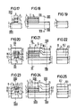
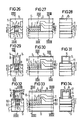
- FIGS. 5 to 34 Three successive figures arranged next to one another each show cross and longitudinal sections in one step of the manufacturing process.
- the first figure on the left shows the cross section corresponding to FIG. 3 through the laser diode L.
- the middle figure shows the longitudinal section corresponding to FIG. 2 through the transition from the laser diode to the passive waveguide.
- the third figure on the right shows a cross section through the switched (corresponding to FIG. 4) or an unswitched region of the waveguide W (one web in each case).
- the buffer layer 2, the etch stop layer 3, the first grating layer 4 and a first protective layer 21 are successively grown on the substrate 1 (FIGS. 5 to 7). Following this epitaxial step, the first protective layer 21 is removed and the surface of the first grating layer 4 is structured with a grating 22 in the region of the laser diode L to be produced (FIG. 8 until 10).
- a first protective layer 21 for example InGaAsP with a cut-off wavelength of 1.3 ⁇ m
- a second lattice layer 5 leveling the lattice 22, the active layer 6, at least one anti-melt-back layer 7, optionally the further anti-melt-back layer 8 and one are successively applied to this first lattice layer 4 second protective layer 23, the z. B. may have the same material composition as the first protective layer 21, grown (see FIGS. 11 to 13).
- the first lattice layer 4, the second lattice layer 5, the active layer 6, the anti-melt-back layer 7 and, if appropriate, the further anti-melt-back layer 8 are outside of those for the production of Areas provided by laser diodes L are etched away. If necessary, marks are set for working with a projection exposure machine mentioned above.
- the cross-sectional profile of this layer sequence provided for the laser diode 11 shown in FIG. 14 is etched in a subsequent step by reactive ion beam etching (RIBE) to the exact width of the laser strip to be produced. This etching takes place at least as far as the surface of the buffer layer 2, the etching stop layer 3 being completely removed in the regions immediately adjacent to the laser strips.
- RIBE reactive ion beam etching
- upper layer portions of the buffer layer 2 can also be etched off in the areas to the side of the laser strip. In this etching step, at least the areas provided for the passive waveguide W are covered with a mask.
- the layer sequence in the area of the laser diode then receives the cross-sectional profile, as shown in FIG. 17.
- the transition from the laser diode into the region of the passive waveguide is at the lateral boundary of that provided for the laser diode Layer sequence recognizable.
- the height H of this layer sequence above the etch stop layer 3 in the area of the laser diode is approximately 0.6 ⁇ m.
- the width B of the laser strip is reduced in the RIBE process step from approx. 50 ⁇ m to approx. 1.5 ⁇ m.
- the first waveguide layer 10.1, the second waveguide layer 10.2, the first cladding layer 11 and a third protective layer 24 are grown (see FIGS. 20 to 22).
- the first cladding layer 11 is removed in the region of the laser web (see FIG. 23).
- the surface of the uppermost layer provided for the laser diode (anti-melt-back layer 7 or, if present, further anti-melt-back layer 8) is exposed.
- a lateral portion of each of the waveguide layers 10.1, 10.2 remains.
- 23 shows the cross section after the removal of the first cladding layer 11 on the laser strip.
- the longitudinal section corresponding to FIG. 24 shows the transition from the laser diode to the waveguide layers 10.1, 10.2.
- the leveling second cladding layer 15 and the contact layer 9 are grown over the entire surface.
- the layer structure after this manufacturing step is shown in FIGS. 26 to 28.
- a flat zinc diffusion is carried out and the contact layer 9 is removed in the area provided as passive.
- the zinc diffusion serves to dope the semiconductor material in the area so high that a metal contact applied thereon forms an ohmic contact (in contrast to a Schottky contact).
- the amount of the doping is a few 1019 cm ⁇ 3.
- This zinc diffusion can be carried out in such a way that a zinc-containing film (for example zinc oxide) is applied and Zn is diffused into the semiconductor material by brief heating.
- the film is then removed.
- the waveguide bars are formed and adjusted on the laser strip in the area of the laser diode.
- the passivation layer 14 is then applied, which can be done, for example, by sputtering. This passivation layer 14 is opened in the areas provided for contacting.
- the first metallization 12 is applied and structured.
- the second metallization 13 is on the bottom of the substrate evaporated over the entire surface.
- FIGS. 29 to 31 show a cross section through the waveguide at a point in the passive region.
- the contact layer 9 has been removed in this passive region and the passivation layer 14 has been applied continuously to the surface of the waveguide web.
- FIGS. 32 and 33 show the first metallization 12 and the second metallization 13 in addition to the structure corresponding to FIGS. 29 and 30. While FIG. 31 shows a cross section through the waveguide in its passive area, FIG. 34 shows the cross section corresponding to FIG. 4 through an active part of the switch S.
- the passivation layer 14 on the top of the web is interrupted and the first metallization 12 applied thereon is in contact with the surface of the contact layer 9.
- the first metallization 12 consists of at least two parts which are electrically insulated from one another, one of which is used for the electrical connection of the laser diode L and the other for the electrical connection of the active part of the switch S. These portions can each be structured on the contacted area of the contact layer 9, the associated connection area and conductive connections (conductor tracks) between the contacted area of the contact layer 9 and the associated connection area.
- An alternative of this manufacturing method provides for using SiO2 in the process step of reactive ion beam etching of the laser strip as etching mask and then leaving it on the laser web.
- the waveguide layers that are grown in the subsequent process step and the first cladding layer 11 do not grow in the case above the SiO2 etching mask on the web. It is therefore not necessary to subsequently remove the first cladding layer 11 and the waveguide layers 10.1, 10.2 above the laser strip. After the etching mask has been removed from the laser strip, the second cladding layer 15 can then be grown directly.
- the present invention has the advantages of an easy to manufacture structure and a direct coupling (butt coupling) of the light generated in the laser diode into the waveguide.
- the properties and functionality of such a circuit have thus been significantly improved compared to the prior art.
Landscapes
- Physics & Mathematics (AREA)
- Condensed Matter Physics & Semiconductors (AREA)
- General Physics & Mathematics (AREA)
- Electromagnetism (AREA)
- Optics & Photonics (AREA)
- Optical Integrated Circuits (AREA)
- Semiconductor Lasers (AREA)
Applications Claiming Priority (2)
| Application Number | Priority Date | Filing Date | Title |
|---|---|---|---|
| DE4014234 | 1990-05-03 | ||
| DE4014234 | 1990-05-03 |
Publications (2)
| Publication Number | Publication Date |
|---|---|
| EP0454902A2 true EP0454902A2 (fr) | 1991-11-06 |
| EP0454902A3 EP0454902A3 (en) | 1992-03-18 |
Family
ID=6405652
Family Applications (1)
| Application Number | Title | Priority Date | Filing Date |
|---|---|---|---|
| EP19900123353 Withdrawn EP0454902A3 (en) | 1990-05-03 | 1990-12-05 | Monolithically integrated circuit with dfb laser diode, optical switch and waveguide connections |
Country Status (1)
| Country | Link |
|---|---|
| EP (1) | EP0454902A3 (fr) |
Cited By (4)
| Publication number | Priority date | Publication date | Assignee | Title |
|---|---|---|---|---|
| DE4142340A1 (de) * | 1991-12-20 | 1993-06-24 | Siemens Ag | Optoelektronischer ic |
| EP0602725A3 (en) * | 1992-12-16 | 1994-09-28 | Koninkl Philips Electronics Nv | Method of manufacturing an optoelectronic semiconductor device. |
| WO1996037020A1 (fr) * | 1995-05-18 | 1996-11-21 | Siemens Aktiengesellschaft | Procede de production d'une diode laser a retroaction repartie (dfb) a guide d'ondes couple et structure a couches pour diode laser a retroaction repartie |
| FR2768232A1 (fr) * | 1997-09-11 | 1999-03-12 | Alsthom Cge Alcatel | Procede de fabrication d'un composant optique integre comprenant un guide d'onde epais couple a un guide d'onde mince |
Family Cites Families (3)
| Publication number | Priority date | Publication date | Assignee | Title |
|---|---|---|---|---|
| DE3580738D1 (de) * | 1984-10-03 | 1991-01-10 | Siemens Ag | Verfahren zur integrierten herstellung eines dfb-lasers mit angekoppeltem streifenwellenleiter auf einem substrat. |
| JP2587628B2 (ja) * | 1987-01-29 | 1997-03-05 | 国際電信電話株式会社 | 半導体集積発光素子 |
| US5147825A (en) * | 1988-08-26 | 1992-09-15 | Bell Telephone Laboratories, Inc. | Photonic-integrated-circuit fabrication process |
-
1990
- 1990-12-05 EP EP19900123353 patent/EP0454902A3/de not_active Withdrawn
Cited By (7)
| Publication number | Priority date | Publication date | Assignee | Title |
|---|---|---|---|---|
| DE4142340A1 (de) * | 1991-12-20 | 1993-06-24 | Siemens Ag | Optoelektronischer ic |
| EP0602725A3 (en) * | 1992-12-16 | 1994-09-28 | Koninkl Philips Electronics Nv | Method of manufacturing an optoelectronic semiconductor device. |
| WO1996037020A1 (fr) * | 1995-05-18 | 1996-11-21 | Siemens Aktiengesellschaft | Procede de production d'une diode laser a retroaction repartie (dfb) a guide d'ondes couple et structure a couches pour diode laser a retroaction repartie |
| US6067312A (en) * | 1995-05-18 | 2000-05-23 | Siemens Aktiengesellschaft | Method for production of a DFB laser diode having a coupled optical waveguide and a DFB laser diode layer structure |
| FR2768232A1 (fr) * | 1997-09-11 | 1999-03-12 | Alsthom Cge Alcatel | Procede de fabrication d'un composant optique integre comprenant un guide d'onde epais couple a un guide d'onde mince |
| EP0902306A1 (fr) * | 1997-09-11 | 1999-03-17 | Alcatel | Procédé de fabrication d'un composant optique intégré comprenant un guide d'onde épais couplé à un guide d'onde mince |
| US6040246A (en) * | 1997-09-11 | 2000-03-21 | Alcatel | Method of manufacturing an integrated optical component comprising a thick waveguide coupled to a thin waveguide |
Also Published As
| Publication number | Publication date |
|---|---|
| EP0454902A3 (en) | 1992-03-18 |
Similar Documents
| Publication | Publication Date | Title |
|---|---|---|
| EP0487876B1 (fr) | Combinaison d'une diode laser et d'un guide d'onde intégré monolithique | |
| EP0849847B1 (fr) | Elément optoélectronique avec une structure MQW | |
| DE19545164B4 (de) | Optische Halbleitervorrichtung mit vergrabenem Wellenleiter und Herstellungsverfahren dafür | |
| EP0187198B1 (fr) | Procédé pour la fabrication d'une structure optique intégrée | |
| DE3787769T2 (de) | Halbleiterlaservorrichtung. | |
| EP0906646B1 (fr) | Combinaison monolithique d'une diode laser et d'un modulateur | |
| DE10157233B4 (de) | Halbleitervorrichtung und die Halbleitervorrichtung verwendende photonische Halbleitervorrichtung sowie ein Verfahren zu deren Herstellung | |
| DE3300986A1 (de) | Mehrschichtige optische integrierte schaltung | |
| DE69717973T2 (de) | Vergrabene heterostruktur | |
| DE19619533A1 (de) | Monolithisch integriertes optisches Halbleiterbauelement | |
| DE69407507T2 (de) | Halbleitende optische Vorrichtung mit Mesa-Struktur, die seitlich von einer isolierenden Maske umgeben ist | |
| EP0383958B1 (fr) | Laser à semi-conducteur accordable | |
| EP0524459B1 (fr) | Laser accordable à semi-conducteur sur un substrat semi-isolant | |
| EP0416477A2 (fr) | Laser à semi-conducteur | |
| DE69319317T2 (de) | Halbleiterlaser und Herstellungsverfahren | |
| DE19945134A1 (de) | Lichtemittierendes Halbleiterbauelement hoher ESD-Festigkeit und Verfahren zu seiner Herstellung | |
| DE69308082T2 (de) | Halbleiterlaservorrichtung | |
| DE3934998A1 (de) | Elektrisch wellenlaengenabstimmbarer halbleiterlaser | |
| DE69123709T2 (de) | Optoelektronische integrierte Schaltung mit einem Langwellensender | |
| DE69113471T2 (de) | Auf einer strukturierten Substratoberfläche aufgewachsene Halbleiter-Laserdiode. | |
| EP0477604B1 (fr) | Coupleur optique directionnel intégré, commandable | |
| EP0454902A2 (fr) | Circuit monolithique intégrÀ© avec diode à laser DFB, commutateur optique et connexions en guide d'onde | |
| DE3020251C2 (fr) | ||
| DE60204702T2 (de) | Verbesserungen für optische vorrichtungen | |
| DE69315811T2 (de) | Verfahren zur Herstellung einer optoelektrischen Halbleitervorrichtung |
Legal Events
| Date | Code | Title | Description |
|---|---|---|---|
| PUAI | Public reference made under article 153(3) epc to a published international application that has entered the european phase |
Free format text: ORIGINAL CODE: 0009012 |
|
| 17P | Request for examination filed |
Effective date: 19901220 |
|
| AK | Designated contracting states |
Kind code of ref document: A2 Designated state(s): DE FR GB IT |
|
| PUAL | Search report despatched |
Free format text: ORIGINAL CODE: 0009013 |
|
| AK | Designated contracting states |
Kind code of ref document: A3 Designated state(s): DE FR GB IT |
|
| STAA | Information on the status of an ep patent application or granted ep patent |
Free format text: STATUS: THE APPLICATION IS DEEMED TO BE WITHDRAWN |
|
| 18D | Application deemed to be withdrawn |
Effective date: 19940701 |