EP0454860B1 - Spannungsfühler mit elektrooptischem kristall sowie verfahren zur spannungsmessung - Google Patents
Spannungsfühler mit elektrooptischem kristall sowie verfahren zur spannungsmessung Download PDFInfo
- Publication number
- EP0454860B1 EP0454860B1 EP90916382A EP90916382A EP0454860B1 EP 0454860 B1 EP0454860 B1 EP 0454860B1 EP 90916382 A EP90916382 A EP 90916382A EP 90916382 A EP90916382 A EP 90916382A EP 0454860 B1 EP0454860 B1 EP 0454860B1
- Authority
- EP
- European Patent Office
- Prior art keywords
- compound semiconductor
- resistance compound
- potential
- sensor
- low
- Prior art date
- Legal status (The legal status is an assumption and is not a legal conclusion. Google has not performed a legal analysis and makes no representation as to the accuracy of the status listed.)
- Expired - Lifetime
Links
- 239000013078 crystal Substances 0.000 title claims description 29
- 238000000034 method Methods 0.000 title claims description 3
- 150000001875 compounds Chemical class 0.000 claims abstract description 60
- 239000004065 semiconductor Substances 0.000 claims abstract description 55
- 238000005259 measurement Methods 0.000 claims description 13
- 239000000758 substrate Substances 0.000 claims description 7
- 230000010287 polarization Effects 0.000 claims description 4
- 230000001678 irradiating effect Effects 0.000 claims description 2
- 230000003287 optical effect Effects 0.000 abstract description 17
- 239000000523 sample Substances 0.000 abstract description 4
- 230000006866 deterioration Effects 0.000 abstract description 2
- 230000005684 electric field Effects 0.000 description 8
- 239000010408 film Substances 0.000 description 6
- 230000035945 sensitivity Effects 0.000 description 5
- -1 GaAs Chemical class 0.000 description 4
- 229910003327 LiNbO3 Inorganic materials 0.000 description 4
- 229910001218 Gallium arsenide Inorganic materials 0.000 description 3
- 229910004613 CdTe Inorganic materials 0.000 description 2
- VYPSYNLAJGMNEJ-UHFFFAOYSA-N Silicium dioxide Chemical compound O=[Si]=O VYPSYNLAJGMNEJ-UHFFFAOYSA-N 0.000 description 2
- 229910007709 ZnTe Inorganic materials 0.000 description 2
- 239000000969 carrier Substances 0.000 description 2
- 239000004020 conductor Substances 0.000 description 2
- 238000001514 detection method Methods 0.000 description 2
- 238000010438 heat treatment Methods 0.000 description 2
- 125000005842 heteroatom Chemical group 0.000 description 2
- 239000012535 impurity Substances 0.000 description 2
- 238000002488 metal-organic chemical vapour deposition Methods 0.000 description 2
- SBIBMFFZSBJNJF-UHFFFAOYSA-N selenium;zinc Chemical compound [Se]=[Zn] SBIBMFFZSBJNJF-UHFFFAOYSA-N 0.000 description 2
- 229910021589 Copper(I) bromide Inorganic materials 0.000 description 1
- 229910021591 Copper(I) chloride Inorganic materials 0.000 description 1
- 229910002601 GaN Inorganic materials 0.000 description 1
- 229910005540 GaP Inorganic materials 0.000 description 1
- 229910000673 Indium arsenide Inorganic materials 0.000 description 1
- 229910007475 ZnGeP2 Inorganic materials 0.000 description 1
- 239000000853 adhesive Substances 0.000 description 1
- 230000001070 adhesive effect Effects 0.000 description 1
- UHYPYGJEEGLRJD-UHFFFAOYSA-N cadmium(2+);selenium(2-) Chemical compound [Se-2].[Cd+2] UHYPYGJEEGLRJD-UHFFFAOYSA-N 0.000 description 1
- WUKWITHWXAAZEY-UHFFFAOYSA-L calcium difluoride Chemical compound [F-].[F-].[Ca+2] WUKWITHWXAAZEY-UHFFFAOYSA-L 0.000 description 1
- 229910001634 calcium fluoride Inorganic materials 0.000 description 1
- 229910052681 coesite Inorganic materials 0.000 description 1
- OXBLHERUFWYNTN-UHFFFAOYSA-M copper(I) chloride Chemical compound [Cu]Cl OXBLHERUFWYNTN-UHFFFAOYSA-M 0.000 description 1
- 229910052906 cristobalite Inorganic materials 0.000 description 1
- 239000002019 doping agent Substances 0.000 description 1
- 230000000694 effects Effects 0.000 description 1
- 238000010894 electron beam technology Methods 0.000 description 1
- 238000005516 engineering process Methods 0.000 description 1
- 229910052732 germanium Inorganic materials 0.000 description 1
- 239000011521 glass Substances 0.000 description 1
- WPYVAWXEWQSOGY-UHFFFAOYSA-N indium antimonide Chemical compound [Sb]#[In] WPYVAWXEWQSOGY-UHFFFAOYSA-N 0.000 description 1
- RPQDHPTXJYYUPQ-UHFFFAOYSA-N indium arsenide Chemical compound [In]#[As] RPQDHPTXJYYUPQ-UHFFFAOYSA-N 0.000 description 1
- 238000004519 manufacturing process Methods 0.000 description 1
- 239000000463 material Substances 0.000 description 1
- 229910052711 selenium Inorganic materials 0.000 description 1
- 238000007493 shaping process Methods 0.000 description 1
- 229910052710 silicon Inorganic materials 0.000 description 1
- 239000000377 silicon dioxide Substances 0.000 description 1
- 235000012239 silicon dioxide Nutrition 0.000 description 1
- 238000004544 sputter deposition Methods 0.000 description 1
- 229910052682 stishovite Inorganic materials 0.000 description 1
- 229910052717 sulfur Inorganic materials 0.000 description 1
- 229910052714 tellurium Inorganic materials 0.000 description 1
- 239000010409 thin film Substances 0.000 description 1
- 229910052718 tin Inorganic materials 0.000 description 1
- 229910052905 tridymite Inorganic materials 0.000 description 1
- 238000007740 vapor deposition Methods 0.000 description 1
- 229910052725 zinc Inorganic materials 0.000 description 1
Images


Classifications
-
- G—PHYSICS
- G01—MEASURING; TESTING
- G01R—MEASURING ELECTRIC VARIABLES; MEASURING MAGNETIC VARIABLES
- G01R1/00—Details of instruments or arrangements of the types included in groups G01R5/00 - G01R13/00 and G01R31/00
- G01R1/02—General constructional details
- G01R1/06—Measuring leads; Measuring probes
- G01R1/067—Measuring probes
- G01R1/07—Non contact-making probes
- G01R1/071—Non contact-making probes containing electro-optic elements
-
- G—PHYSICS
- G01—MEASURING; TESTING
- G01R—MEASURING ELECTRIC VARIABLES; MEASURING MAGNETIC VARIABLES
- G01R15/00—Details of measuring arrangements of the types provided for in groups G01R17/00 - G01R29/00, G01R33/00 - G01R33/26 or G01R35/00
- G01R15/14—Adaptations providing voltage or current isolation, e.g. for high-voltage or high-current networks
- G01R15/24—Adaptations providing voltage or current isolation, e.g. for high-voltage or high-current networks using light-modulating devices
- G01R15/241—Adaptations providing voltage or current isolation, e.g. for high-voltage or high-current networks using light-modulating devices using electro-optical modulators, e.g. electro-absorption
- G01R15/242—Adaptations providing voltage or current isolation, e.g. for high-voltage or high-current networks using light-modulating devices using electro-optical modulators, e.g. electro-absorption based on the Pockels effect, i.e. linear electro-optic effect
Definitions
- the present invention relates to a potential measuring apparatus employing an electrooptic crystal, in which the potential of an object is measured by making use of the fact that the optical anisotropy of an electrooptic crystal changes with the electric field.
- the present invention also relates to a potential measuring method carried out by use of such a potential measuring apparatus.
- an electrooptic crystal 1 is brought close to an object 3 of measurement, with a transparent electrode 2 bonded to the crystal 1 and grounded. Assuming that the object 3 has a predetermined surface potential, lines of electric force from the object 3 terminate at the electrode 2 through the electrooptic crystal 1 and a predetermined electric field is therefore applied to the electrooptic crystal 1, resulting in a change in the optical anisotropy. Since the change in the optical anisotropy is proportional to the magnitude of the electric field, if polarized light 4, for example, is applied, the polarization of the reflected or transmitted light changes.
- This type of optical potential sensor has heretofore been produced by forming a transparent electrode (ITO) 2 on a glass substrate 6 by sputtering or the like, as shown in Fig. 6, bonding LiNbO3 1 to the surface of the transparent electrode 2 by means of an adhesive 7, grinding the LiNbO3 1 to a necessary thickness, and then forming a dielectric reflecting film 8 thereon by use of thin-film technology.
- the conventional optical potential sensor has a complicated structure.
- the bonding step and the grinding step are involved, the production process is complicated and the processing characteristics are inferior. Further, the surface accuracy is low because of the thickness unevenness that is caused by the bonding and the grinding, which results in low measuring accuracy.
- LiNbO3 since LiNbO3 has optical properties which are different in all of the three directions, it is difficult to incline the Z-axis of the crystal exactly at 55° with respect to the direction of incidence of light. Further, LiNbO3 involves the problem of photo-deterioration.
- the potential sensor of the present invention is characterized by measuring a potential by use of an electrooptic crystal comprising a high-resistance compound semiconductor layer which is formed on a low-resistance compound semiconductor substrate by epitaxial growth.
- the potential sensor of the present invention is characterized in that the low-resistance compound semiconductor and the high-resistance compound semiconductor each have a large bandgap.
- the potential sensor of the present invention is characterized in that a dielectric reflecting film is formed on the high-resistance compound semiconductor layer.
- the potential sensor of the present invention is characterized by being disposed close and in opposing relation to an object of measurement, with the low-resistance compound semiconductor substrate grounded, irradiating the object with linearly, elliptically or circularly polarized light, and measuring the potential of the object from a change in the polarization of light.
- Fig. 1 shows the arrangement of the sensor according to the present invention.
- reference numeral 10 denotes a sensor body, 11 a low-resistance compound semiconductor, 12 a high-resistance compound semiconductor, and 13 a dielectric reflecting film.
- the present invention has been accomplished by noting that a compound semiconductor optically causes double refraction when placed in an electric field and it suffers almost no deterioration by light and that a low-resistance compound semiconductor functions as a conductor.
- a high-resistance compound semiconductor 12 is epitaxially grown on a low-resistance compound semiconductor wafer and a dielectric reflecting film 13 is formed thereon, thereby forming a monolithic sensor.
- the low-resistance compound semiconductor 11 is required to transmit probe light without absorbing it and therefore desired to have a large bandgap and also have a lattice constant and a thermal expansion coefficient, which are close to those of the high-resistance compound semiconductor which is epitaxially grown thereon.
- the resistivity thereof is preferably 10+1 ⁇ cm or less.
- Examples of compound semiconductors which are usable as the high-resistance compound semiconductor 12 are non-doped compound semiconductors and compound semiconductors doped with a dopant having a deep level so as to have a high resistance, such as GaAs doped with Cr and CdTe doped with Cl.
- the high-resistance compound semiconductor 12 is desired to have a large bandgap so that light of short wavelength can be used, and it is also desired to have a large electrooptic constant. Since it is desired to apply a large electric field, it is preferable that the high-resistance compound semiconductor 12 have a resistivity of 105 ⁇ cm or more.
- Usable compound semiconductors are III-V group compounds, e.g., GaAs, GaP, GaN, InAs, InSb, etc., or a mixed crystal of these compounds, II-VI group compounds, e.g., ZnS, ZnSe, CdS, CdSe, CdTe, ZnTe, etc., or a mixed crystal of these compounds, and I-VII group compounds, e.g., CuCl, CuBr, etc., or a mixed crystal of these compounds.
- a III-V group compound e.g., P-type GaAs is doped with Zn, Mg, Mn or Be to form a low-resistance compound semiconductor
- N-type GaP is doped with S, Se, Te, Si, Ge or Sn to form a low-resistance compound semiconductor
- a II-VI group compound e.g., ZnS or ZnSe is doped with Li or N to form a P-type low-resistance compound semiconductor, or it is doped with Cl to form an N-type low-resistance compound semiconductor.
- I-III-VI2 group compounds e.g., CuGaS2, CuAlSe2, etc., or a mixed crystal of these compounds
- II-VI-V2 group compounds e.g., ZnSiP2, ZnGeP2, CdSiP2, etc., or a mixed crystal of these compounds.
- the low-resistance compound semiconductor and the high-resistance compound semiconductor may form either a homo structure or hetero structure. Since the low- and high-resistance compound semiconductors are assigned different functions, if materials which are suitable for the respective functions are used, a hetero structure is formed, in general.
- the carriers act to cancel the external electric field and hence weakens the electric field in the high-resistance compound semiconductor, resulting in a lowering of the detecting sensitivity.
- the high-resistance compound semiconductor In order to prevent the lowering of the sensitivity, the high-resistance compound semiconductor must be prevented from being exposed to light that generates photocarriers. It is also necessary to prevent the high-resistance compound semiconductor from heating up to a temperature at which thermocarriers are generated.
- the present invention has been described by way of one example in which potential measurement is effected by use of reflected light, it should be noted that potential measurement can be similarly effected by use of transmitted light. In such a case, no dielectric reflecting film is needed, as a matter of course, and the object of measurement also needs to transmit the light for measurement.
- Fig. 2 shows the arrangement of one embodiment of a potential measuring apparatus employing the sensor of the present invention.
- Linearly polarized light from a laser diode 20 is collimated through a condenser lens 21 and applied to the sensor 10 of the present invention through a half-mirror 22 and an objective lens 23.
- the optical anisotropy of the sensor 10 changes with the potential of an object 24 of measurement that is disposed in opposing relation and close proximity to the sensor 10.
- a reflected light component in a predetermined optical axis direction causes a retardataion, resulting in elliptically polarized light.
- the elliptically polarized light is reflected from the half-mirror 22 and passed through, for example, a halfwave plate 25 whereby the component retarded by the sensor 10 and a component orthogonal thereto are mixed together, and the resulting light is divided by a polarization beam splitter 26 into two beams, which are condensed through respective lenses 27 and 28 and detected by respective light-receiving elements 29 and 30.
- the detection outputs are amplified in a differential amplifier 31.
- the output of the differential amplifier 31 is proportional to sin( ⁇ + ⁇ ) where ⁇ is given by the expression (1), and ⁇ is a phase factor.
- a potential range in which the linearity is required can be determined by disposing a proper phase compensator in the optical path, for example, in between the condenser lens 21 and the half-mirror 22 and moving ⁇ .
- a beam shaping prism should be inserted in the optical path, for example, in between the condenser lens 21 and the half-mirror 22.
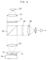
- Fig. 3 shows the arrangement of another embodiment of a potential measuring apparatus employing the sensor of the present invention.
- the output of the potential measuring apparatus is proportional to sin2( ⁇ + ⁇ ) The sensitivity of this apparatus is lower than that of the apparatus shown in Fig. 1.
- the apparatuses shown in Figs. 2 and 3 can measure the potential at one position on the object of measurement, and when the entire surface of the object is to be continuously measured, the entire surface must be scanned with the optical system and the object being moved relative to each other.
- the electrooptic crystal of the sensor section may be stationary relative to the optical system or relative to the object.
- the electrooptic crystal becomes thinner, the resolution becomes higher, and the numerical aperture of the objective lens must be optimized.
- the sensitivity becomes higher as the electrooptic crystal becomes thicker.
- the sensitivity is incompatible with the resolution.
- gap control may be effected by use of a servo mechanism.
- the gap control can be effected by moving either or both the object and the electrooptic crystal.
- the electrooptic crystal is also moved, it is necessary to receive the reflected light from the electrooptic crystal with divided photodiodes and effect focusing on the electrooptic crystal by feedback-controlling the servo mechanism such that the difference between the quantities of light received by the photodiodes is minimized.
- High-resistance ZnTe was epitaxially grown to a thickness of 20»m by MOCVD on a low-resistance compound semiconductor substrate (100) made of GaP and having a thickness of 300»m.
- a conductor 40 from a power supply V, as shown in Fig. 4
- an output change of 1% with respective to the incident light intensity was detected by the measuring apparatus shown in Fig. 2.
- High-resistance CuGaS2 was epitaxially grown to a thickness of 10»m on a low-resistance GaP (100) substrate by MOCVD, and a multilayer dielectric reflecting film of SiO2 and CaF2 was formed thereon by vapor deposition by electron-beam heating.
- the double refraction of a compound semiconductor is utilized, and a high-resistance compound semiconductor is epitaxially grown on a semiconductor doped with impurities so as to have a low resistance. It is therefore possible to form a sensor which has excellent processing characteristics, extremely high surface accuracy and minimal photo-deterioration.
- the present invention can be utilized to measure the potential of an object, particularly, to read with high accuracy an electrostatic image on an electric charge retaining medium recorded by exposing it to an optical image under the application of a voltage.
Landscapes
- Physics & Mathematics (AREA)
- General Physics & Mathematics (AREA)
- Measuring Instrument Details And Bridges, And Automatic Balancing Devices (AREA)
- Measurement Of Current Or Voltage (AREA)
Claims (4)
- Spannungsfühler (10) mit einem elektrooptischen Kristall umfassend eine Verbindungshalbleiterschicht (12) mit hohem Widerstand, die durch epitaxiales Wachsen auf einem Verbindungshalbleitersubstrat (11) mit niedrigem Widerstand gebildet ist.
- Spannungsfühler (10) mit einem elektrooptischen Kristall nach Anspruch 1, wobei der Verbindungshalbleiter (11) mit niedrigem Widerstand und der Verbindungshalbleiter (12) mit hohem Widerstand jeweils eine große Bandlücke aufweisen.
- Spannungsfühler (10) mit einem elektrooptischen Kristall nach Anspruch 1 oder 2, wobei ein dielektrischer Reflektionsfilm (13) auf der Verbindungshalbleiterschicht (12) mit hohem Widerstand gebildet ist.
- Verfahren zur Spannungsmessung umfassend: Anordnung des Fühlers (10) nach einem der Ansprüche 1 bis 3 nahe und in Gegenüberstellung zu dem Meßobjekt, wobei das Verbindungshalbleitersubstrat (11) mit niedrigem Widerstand geerdet ist, Bestrahlung des Objekts mit linear polarisiertem, elliptisch polarisiertem oder kreispolarisiertem Licht und Messen der Spannung des Objekts durch eine Änderung im Polarisationszustand des Lichts.
Applications Claiming Priority (3)
| Application Number | Priority Date | Filing Date | Title |
|---|---|---|---|
| JP1294367A JPH03154875A (ja) | 1989-11-13 | 1989-11-13 | 電気光学結晶を用いた電位センサ及び電位測定方法 |
| JP294367/89 | 1989-11-13 | ||
| PCT/JP1990/001466 WO1991007666A1 (fr) | 1989-11-13 | 1990-11-13 | Capteur de potentiel utilisant un cristal electro-optique et procede de mesure de potentiel |
Publications (3)
| Publication Number | Publication Date |
|---|---|
| EP0454860A1 EP0454860A1 (de) | 1991-11-06 |
| EP0454860A4 EP0454860A4 (en) | 1992-08-19 |
| EP0454860B1 true EP0454860B1 (de) | 1995-03-01 |
Family
ID=17806795
Family Applications (1)
| Application Number | Title | Priority Date | Filing Date |
|---|---|---|---|
| EP90916382A Expired - Lifetime EP0454860B1 (de) | 1989-11-13 | 1990-11-13 | Spannungsfühler mit elektrooptischem kristall sowie verfahren zur spannungsmessung |
Country Status (4)
| Country | Link |
|---|---|
| EP (1) | EP0454860B1 (de) |
| JP (1) | JPH03154875A (de) |
| DE (1) | DE69017431T2 (de) |
| WO (1) | WO1991007666A1 (de) |
Families Citing this family (9)
| Publication number | Priority date | Publication date | Assignee | Title |
|---|---|---|---|---|
| US5714345A (en) * | 1990-12-24 | 1998-02-03 | Pharmaceutical Proteins Limited | Increased expression of a gene by a second transferred mammary gland specific sequence transgenic |
| DE4205509A1 (de) * | 1992-02-24 | 1993-08-26 | Mwb Pruefsysteme Gmbh | Verfahren und sensor zum messen von elektrischen spannungen und/oder elektrischen feldstaerken |
| US5406194A (en) * | 1992-09-21 | 1995-04-11 | At&T Corp. | Alx Ga1-x as probe for use in electro-optic sampling |
| EP0622708B1 (de) * | 1993-04-26 | 2000-07-12 | Dai Nippon Printing Co., Ltd. | Photoelektrische Sensor, Aufzeichnungssystem, und Verfahren für Datenaufzeichnung und Reprographie |
| EP0668507B1 (de) * | 1993-07-07 | 2002-10-09 | NEC TOKIN Corporation | Fühler für elektrische felder |
| DE4416298A1 (de) * | 1994-05-09 | 1995-11-16 | Abb Research Ltd | Verfahren und Vorrichtung zur optischen Ermittlung einer physikalischen Größe |
| GB9413179D0 (en) * | 1994-06-30 | 1994-09-28 | Univ Surrey | Optical sensors |
| DE29707379U1 (de) * | 1997-04-24 | 1997-06-19 | PMK Mess- und Kommunikationstechnik GmbH, 63150 Heusenstamm | Gerät zur Messung von Hochspannung an Hochspannungsleitungen |
| JP4624648B2 (ja) * | 2003-02-07 | 2011-02-02 | Jx日鉱日石金属株式会社 | 電気光学素子用CdTe系化合物半導体単結晶 |
Family Cites Families (4)
| Publication number | Priority date | Publication date | Assignee | Title |
|---|---|---|---|---|
| FR1499441A (fr) * | 1966-09-16 | 1967-10-27 | Electronique & Physique | Procédé et dispositif de transmission d'informations sur faisceau lumineux |
| DE2311469C2 (de) * | 1973-03-08 | 1986-09-04 | Siemens AG, 1000 Berlin und 8000 München | Lichtmodulationseinrichtung mit Schottky-Kontakt |
| JPS56150724A (en) * | 1980-04-23 | 1981-11-21 | Nippon Telegr & Teleph Corp <Ntt> | Optical frequency modulator |
| JPS62198830A (ja) * | 1986-02-26 | 1987-09-02 | Hitachi Ltd | 光変調器 |
-
1989
- 1989-11-13 JP JP1294367A patent/JPH03154875A/ja active Pending
-
1990
- 1990-11-13 DE DE69017431T patent/DE69017431T2/de not_active Expired - Fee Related
- 1990-11-13 WO PCT/JP1990/001466 patent/WO1991007666A1/ja not_active Ceased
- 1990-11-13 EP EP90916382A patent/EP0454860B1/de not_active Expired - Lifetime
Also Published As
| Publication number | Publication date |
|---|---|
| JPH03154875A (ja) | 1991-07-02 |
| DE69017431D1 (de) | 1995-04-06 |
| DE69017431T2 (de) | 1995-06-29 |
| EP0454860A4 (en) | 1992-08-19 |
| EP0454860A1 (de) | 1991-11-06 |
| WO1991007666A1 (fr) | 1991-05-30 |
Similar Documents
| Publication | Publication Date | Title |
|---|---|---|
| US4563093A (en) | Voltage and electric field measuring device using light | |
| EP0655620B1 (de) | Auf Lichtstreuung basierende Temperaturmessung von Werkstücken in Echtzeit | |
| EP0086373B1 (de) | Magneto-optischer Wandler | |
| US5061072A (en) | Differential ellipsometer | |
| EP0454860B1 (de) | Spannungsfühler mit elektrooptischem kristall sowie verfahren zur spannungsmessung | |
| US5434698A (en) | Potential sensor employing electrooptic crystal and potential measuring method | |
| JPH05249207A (ja) | 光センサ | |
| US3426201A (en) | Method and apparatus for measuring the thickness of films by means of elliptical polarization of reflected infrared radiation | |
| Nagai et al. | Characterization of ultrathin conductive films using a simplified approach for terahertz time-domain spectroscopic ellipsometry | |
| US5737082A (en) | Method of electro-optical measurement for vector components of electric fields and an apparatus thereof | |
| EP0262016A1 (de) | Integrierter Magnetfeldmesskopf und Herstellung dafür | |
| Barns et al. | X-ray determination of polarity sense by anomalous scattering at an absorption edge | |
| US20020085214A1 (en) | Measurement technique for ultra-thin oxides | |
| Cheo | Electro‐optic properties of reverse‐biased GaAs epitaxial thin films at 10.6 μm | |
| Yuan et al. | Polarization measurement method based on liquid crystal variable retarder (LCVR) for atomic thin-film thickness | |
| Miyagawa et al. | Enhanced magneto-optical Kerr effect of GaAs-based pn junctions in the terahertz range | |
| Kim et al. | The improvement of phase modulated spectroscopic ellipsometry | |
| JPH09211035A (ja) | 電界測定装置 | |
| US4128338A (en) | Modified optical transmission technique for characterizing epitaxial layers | |
| Raine et al. | An instrument for measuring the thermal coefficient of refractive index in the infrared | |
| Bayvel | Electro-optic coefficient in BSO-type crystals with optical activity measurement and application to sensors | |
| US20250234784A1 (en) | Photodetector based on transverse dember effect and preparation method thereof | |
| Kuttner et al. | Measuring the homogeneity of infrared materials | |
| Morasca et al. | High accuracy determination of semiconductor substrate and waveguide refractive index by prism coupling | |
| Olivier | Guided-wave optical spectroscopy of thin films |
Legal Events
| Date | Code | Title | Description |
|---|---|---|---|
| PUAI | Public reference made under article 153(3) epc to a published international application that has entered the european phase |
Free format text: ORIGINAL CODE: 0009012 |
|
| 17P | Request for examination filed |
Effective date: 19910808 |
|
| AK | Designated contracting states |
Kind code of ref document: A1 Designated state(s): DE FR GB IT |
|
| A4 | Supplementary search report drawn up and despatched |
Effective date: 19920703 |
|
| AK | Designated contracting states |
Kind code of ref document: A4 Designated state(s): DE FR GB IT |
|
| 17Q | First examination report despatched |
Effective date: 19940301 |
|
| GRAA | (expected) grant |
Free format text: ORIGINAL CODE: 0009210 |
|
| ITF | It: translation for a ep patent filed | ||
| AK | Designated contracting states |
Kind code of ref document: B1 Designated state(s): DE FR GB IT |
|
| ET | Fr: translation filed | ||
| REF | Corresponds to: |
Ref document number: 69017431 Country of ref document: DE Date of ref document: 19950406 |
|
| PLBE | No opposition filed within time limit |
Free format text: ORIGINAL CODE: 0009261 |
|
| STAA | Information on the status of an ep patent application or granted ep patent |
Free format text: STATUS: NO OPPOSITION FILED WITHIN TIME LIMIT |
|
| 26N | No opposition filed | ||
| REG | Reference to a national code |
Ref country code: GB Ref legal event code: IF02 |
|
| PGFP | Annual fee paid to national office [announced via postgrant information from national office to epo] |
Ref country code: GB Payment date: 20031104 Year of fee payment: 14 |
|
| PGFP | Annual fee paid to national office [announced via postgrant information from national office to epo] |
Ref country code: FR Payment date: 20031106 Year of fee payment: 14 |
|
| PGFP | Annual fee paid to national office [announced via postgrant information from national office to epo] |
Ref country code: DE Payment date: 20031203 Year of fee payment: 14 |
|
| PG25 | Lapsed in a contracting state [announced via postgrant information from national office to epo] |
Ref country code: GB Free format text: LAPSE BECAUSE OF NON-PAYMENT OF DUE FEES Effective date: 20041113 |
|
| PG25 | Lapsed in a contracting state [announced via postgrant information from national office to epo] |
Ref country code: DE Free format text: LAPSE BECAUSE OF NON-PAYMENT OF DUE FEES Effective date: 20050601 |
|
| GBPC | Gb: european patent ceased through non-payment of renewal fee |
Effective date: 20041113 |
|
| PG25 | Lapsed in a contracting state [announced via postgrant information from national office to epo] |
Ref country code: FR Free format text: LAPSE BECAUSE OF NON-PAYMENT OF DUE FEES Effective date: 20050729 |
|
| REG | Reference to a national code |
Ref country code: FR Ref legal event code: ST |
|
| PG25 | Lapsed in a contracting state [announced via postgrant information from national office to epo] |
Ref country code: IT Free format text: LAPSE BECAUSE OF NON-PAYMENT OF DUE FEES;WARNING: LAPSES OF ITALIAN PATENTS WITH EFFECTIVE DATE BEFORE 2007 MAY HAVE OCCURRED AT ANY TIME BEFORE 2007. THE CORRECT EFFECTIVE DATE MAY BE DIFFERENT FROM THE ONE RECORDED. Effective date: 20051113 |