EP0454841B1 - Circuit de terminaison pour une echelle r-2r qui compense les ecarts de temperature - Google Patents
Circuit de terminaison pour une echelle r-2r qui compense les ecarts de temperature Download PDFInfo
- Publication number
- EP0454841B1 EP0454841B1 EP91901034A EP91901034A EP0454841B1 EP 0454841 B1 EP0454841 B1 EP 0454841B1 EP 91901034 A EP91901034 A EP 91901034A EP 91901034 A EP91901034 A EP 91901034A EP 0454841 B1 EP0454841 B1 EP 0454841B1
- Authority
- EP
- European Patent Office
- Prior art keywords
- emitter
- transistors
- transistor
- base
- voltage
- Prior art date
- Legal status (The legal status is an assumption and is not a legal conclusion. Google has not performed a legal analysis and makes no representation as to the accuracy of the status listed.)
- Expired - Lifetime
Links
- 230000005284 excitation Effects 0.000 claims abstract description 11
- 238000000034 method Methods 0.000 claims description 10
- 230000008878 coupling Effects 0.000 claims 1
- 238000010168 coupling process Methods 0.000 claims 1
- 238000005859 coupling reaction Methods 0.000 claims 1
- 230000000063 preceeding effect Effects 0.000 claims 1
- 239000003990 capacitor Substances 0.000 abstract description 3
- 230000001419 dependent effect Effects 0.000 description 4
- 238000010586 diagram Methods 0.000 description 4
- 230000006872 improvement Effects 0.000 description 3
- 230000004075 alteration Effects 0.000 description 2
- 230000000694 effects Effects 0.000 description 2
- 238000005516 engineering process Methods 0.000 description 2
- 238000004519 manufacturing process Methods 0.000 description 2
- 238000012986 modification Methods 0.000 description 2
- 230000004048 modification Effects 0.000 description 2
- 238000004458 analytical method Methods 0.000 description 1
- 238000006243 chemical reaction Methods 0.000 description 1
Images

Classifications
-
- H—ELECTRICITY
- H03—ELECTRONIC CIRCUITRY
- H03M—CODING; DECODING; CODE CONVERSION IN GENERAL
- H03M1/00—Analogue/digital conversion; Digital/analogue conversion
- H03M1/06—Continuously compensating for, or preventing, undesired influence of physical parameters
- H03M1/08—Continuously compensating for, or preventing, undesired influence of physical parameters of noise
- H03M1/089—Continuously compensating for, or preventing, undesired influence of physical parameters of noise of temperature variations
-
- H—ELECTRICITY
- H03—ELECTRONIC CIRCUITRY
- H03M—CODING; DECODING; CODE CONVERSION IN GENERAL
- H03M1/00—Analogue/digital conversion; Digital/analogue conversion
- H03M1/66—Digital/analogue converters
- H03M1/74—Simultaneous conversion
- H03M1/78—Simultaneous conversion using ladder network
- H03M1/785—Simultaneous conversion using ladder network using resistors, i.e. R-2R ladders
Definitions
- This invention relates to a digital-to-analog converter (DAC) of the current output type that has a number of transistor current sources connected to an R-2R resistive ladder network, which establishes the current weighting. More particularly, the invention relates to a circuit which is used to terminate the R-2R ladder in a way that equalizes the temperature drift of the base-to-emitter voltages of the current source transistors.
- DAC digital-to-analog converter
- each 2R resistor in the R-2R ladder is connected to the emitter of a bipolar transistor.
- the resistor-transistor combination forms a current source, when the transistor is turned on, contributing a portion of the output current.
- each transistor is identical to its counterparts in the other 2R legs. However, the current in each successive 2R leg is one-half the current of the previous leg.
- This voltage produces, through the series resistors of the ladder, a compensation current which develops corresponding voltage components matching the base-emitter voltage differences ( ⁇ V be ) between successive legs (or stages), so that the voltage across each of the 2R shunt resistors of the ladder remains unaffected by changes in offset voltage due to temperature.
- ⁇ V be base-emitter voltage differences
- Another object of this invention is to provide a compensation circuit which does not need an amplifier.
- Yet another object of the invention is to provide a compensation circuit which is compatible with DAC's that are fabricated using only NPN bipolar technology or only PNP technology.
- the present invention provides a termination circuit for an R-2R resistor ladder network used in a current weighted circuit, as defined in claim 1.
- the invention also provides a method of compensating for differences in the base-emitter voltages between current source transistors of an R-2R resistor ladder, as defined in claim 9.
- the present invention makes use of the theory of U.S.-A-4,349,811 and goes on to teach an improved method and apparatus for terminating an R-2R ladder in a current-switching DAC.
- U.S.-A-4,349,811 varied the usual arrangement of a DAC using an R-2R ladder by connecting the standard 2R terminating resistor of the ladder to an excitation voltage which is 2(kT/q)ln 2 closer to the supply voltage than the emitter of the current source in the last (i.e., least significant) stage.
- the present invention greatly enhances the usefulness of the prior theory by providing excitation source circuitry that is fabricated with just one type of bipolar transistor (e.g., all NPN's or all PNP's), and does not require an amplifier with its attendant frequency compensation capacitor(s).
- the invention improves the accuracy of each binary current source in the R-2R ladder in a way that greatly simplifies the architecture and the fabrication of the improved R-2R DAC.
- the excitation source is a simple circuit requiring only five transistors. At least one of the transistors has an emitter area which is a multiple of the emitter areas of the current source transistors.
- the transistors in the excitation source are connected so that their base-to-emitter voltages are continuously connected in a voltage loop that goes from a voltage V LSB at the emitter of the current source transistor connected to the least significant ladder network shunt resistor to a voltage, Vt, which would be equal to V LSB ' if all six transistors in the loop had the same emitter area, but which deviates thereform by the 2(kT/q)ln 2 compensation voltage due the differences in the emitter areas.
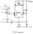
- Fig. 1 shows a portion of a digital-to-analog converter, based on a known type of DAC called a current-mode or current switching converter.
- a current-mode or current switching converter comprises a number of identical transistors 10-1 through 10-n connected as current sources, with their bases tied to a common bias line 12, and their emitters connected to respective shunt resistors 14-1 through 14-n, all of value 2R, along an R-2R ladder 16, having series resistors (18-1, 18-2 ..., 18-n), all of value R.
- the bias line (12) is held fixed at a voltage designated as -V b .
- the collector currents of the transistors 10-1, 10-2, 10-3, ..., 10-n are selectively summed by a summation circuit 24 to produce the desired analog output signal corresponding to an applied digital input signal, as is fully described in the general body of literature on DAC's.
- the output of an operational amplifier 20 applies an excitation voltage to the input terminal 22 of the ladder 16.
- the ladder excitation voltage is controlled by a feedback loop, comprising a reference transistor 26, with its emitter connected through a 2R resistor 28 to the output of the operational amplifier 20.
- the base of this transistor is tied to the common base bias line 12, and the collector is connected to one input terminal of the amplifier.
- a source of constant reference voltage, V REF is also connected to this input terminal.
- the amplifier 20 continuously compares the collector current of transistor 26 with the reference current (i REF ) established in resistor 30, and sets the voltage at node 22 at the lower end of resistor 28 to maintain the collector current equal to the reference current. Since the voltage at node 22 also is applied to the ladder input, the control of that voltage by the amplifier 20 serves also to stabilize the collector currents of the current source transistors 10-1, 10-2, 10-3, ..., 10-n.
- each of the identical source transistors 10-1, 10-2, 10-3, ..., 10-n operates at a different current (i.e., each successive transistor has one-half the current of the previous transistor). Therefore, no two transistors operate at the same current density; hence each has a slightly different base-to-emitter voltage (V be ). Moreover, the differences between these base-to-emitter voltages ( ⁇ V be ) are temperature-dependent, so that it is not possible simply to make a compensating adjustment in the resistor network values which would accommodate the temperature-varying component of the differences from stage to stage.
- Fig. 2 shows a schematic circuit diagram for developing a voltage of 2(kT/q)ln 2 for the 2R termination resistor 32, which supplies the current for the least significant bit's contribution, according to US-A-4 349 811.
- This circuit consists of both NPN transistors (34, 35 and 36) and PNP transistors (37, 38 and 39).
- U.S. Patent No. 4 349 811 (Brokaw) also describes other circuits for accomplishing the same compensation but typically they require either an amplifier or both NPN and PNP transistors.
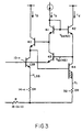
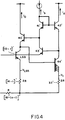
- FIG. 3 A simpler termination circuit, accomplishing the same temperature compensation is shown in Fig. 3. This circuit is simpler to manufacture than any previously shown circuit for achieving the compensation taught in U.S. Patent No. 4 349 811. It does not require an amplifier, and can be fabricated in either all NPN or all PNP type transistors.
- Fig. 3 shows the circuit as it connects to the LSB transistor 10-n in the R-2R ladder of the DAC.
- Transistors 40 through 44 terminate the ladder with a voltage which is (2kt/q)ln2 more positive than the emitter voltage of the LSB transistor 10-n. To see why this is so, consider the continuous path of base-to- emitter voltages (V be 's) from the emitter of transistor 10-n to the emitter of transistor 44.
- V t The voltage at the top of the resistor 32 (i.e., V t ) can be expressed as the sum of base-to-emitter voltages around the loop from V LSB (i.e., the voltage at the top of resistor 14-n) to V t (i.e., the voltage at the top of resistor 32).
- V be(43) , and V be(42) ascend in voltage (i.e., are positive), whereas V be(41) , V be(40) and V be(44) descend (i.e., are negative).
- V LSB + V be(10-n) + V be(43) + V be(42) - V be(41) - V be(40) - V be(44) V t
- V t - V LSB V be(10-n) + V be(43) + V be(42) - V be(41) - V be(40) - V be(44) .
- V t - V LSB (V be(10-n) - V be(40) ) + (V be(43) - V be(41) ) + (V be(42) - V be(44) )
- transistors 10-n and 40 operate at the LSB current so their base-emitter voltages match and the term (V be(10-n) - V be(40) ) drops out as well.
- transistors 42 and 44 operate at the same current (i o ), but since transistor 44 is larger than transistor 42, it operates at a different current density. Therefore, the term involving V be(42) and V be(44) is not zero.
- transistor 40 or 41 may be made with four times the emitter area of the other transistors in the loop, instead of transistor 44, to obtain the same overall result.
- two of the three transistors 40, 41 or 44 each may have twice the emitter area, which will also achieve the same result.
- all three of those transistors could have 4/3 the area of transistor 44 and the other transistors in the loop.
- Other emitter area combinations can be employed, as well, so long as the total base-emitter voltage difference developed around the loop is the required 2(kT/q)ln 2, required to provide the sought after compensation.
- additional junctions may be introduced into the loop, as well, without departing from this teaching, so long as the loop develops the aforementioned base-emitter voltage difference.
- a second error results from the modulation of V be by collector voltage.
- Transistors 41, 43, and 10-n operate at or near zero collector-to-base voltage.
- Transistor 44 has approximately a single base-emitter voltage reverse biasing its collector.
- the collector voltages of 40 and 42 are not constrained by the circuit, as shown. The effects of collector voltage on the two transistors have opposite results on the voltage V t .
Landscapes
- Engineering & Computer Science (AREA)
- Theoretical Computer Science (AREA)
- Analogue/Digital Conversion (AREA)
- Amplifiers (AREA)
- Networks Using Active Elements (AREA)
Abstract
Claims (16)
- Circuit en échelle à résistances R-2R utilisé dans un circuit à pondération de courant, qui possède :(A) une pluralité de transistors (10-1 à 10-n), comportant un transistor de moindre signification (10-n), qui font fonction de sources de courant pour des densités de courant différentes ;(B) le réseau en échelle (16) comportant une résistance parallèle (14-1 à 14-n) associée à chaque source de courant ;(C) les résistances parallèles (14-1 à 14-n) du réseau en échelle (16) étant connectées à des émetteurs sources de courant des transistors (10-1 à 10-n) afin de fournir des courants de transistor pondérés ; et(D) une source d'excitation connectée audit réseau en échelle (16) afin d'engendrer lesdits courants pondérés dans lesdits transistors (10-1 à 10-n) ;(E) ledit réseau en échelle (16) comportant, à l'une de ses extrémités, un circuit de terminaison qui comprend une résistance de terminaison (32) de valeur 2R, et une source de tension qui possède une sortie (Vt) connectée à la résistance de terminaison (32) afin de lui appliquer une tension qui est plus proche, d'une quantité 2(kT/q)log2, d'une tension de sortie que la tension présente sur l'émetteur du transistor de moindre signification (VLSB) du réseau en échelle R-2R, etcaractérisé en ce que :
(F) la source de tension est formée d'une pluralité de transistors (40-44) qui sont tous du même type bipolaire, la pluralité de transistors de la source de tension étant fonctionnellement couplée entre l'émetteur du transistor de moindre signification (10-n) et la sortie de la source de tension (Vt), et comportant :un premier groupe de transistors (43, 42) dont les jonctions base-émetteur sont couplées en série, suivant un premier sens de changement de potentiel par rapport à la base du transistor de moindre signification, à un noeud de référence ; etun deuxième groupe de transistors (40, 41, 44), dont les jonctions base-émetteur sont couplées en série, suivant un deuxième sens de changement de potentiel, opposé au premier sens, par rapport audit noeud de référence, à la sortie de la source de tension (Vt). - Réseau en échelle selon la revendication 1, où on peut sélectionner la tension de sortie en réalisant une aire de surface d'émetteur d'au moins un transistor de la pluralité de transistors qui est différente de celles des autres transistors de la pluralité de transistors.
- Réseau en échelle selon la revendication 2, où :le premier groupe de transistors comporté un premier transistor (43) et un deuxième transistor (42) ; etle deuxième groupe de transistors comporte un troisième transistor (41), un quatrième transistor (40) et un cinquième transistor (44).
- Réseau en échelle selon la revendication 3, où l'aire de l'émetteur de l'un de ces cinq transistors (40-44) vaut quatre fois l'aire d'émetteur du transistor de moindre signification (10-n).
- Réseau en échelle selon la revendication 3, où les aires d'émetteur de deux de ces cinq transistors (40-44) valent chacune deux fois l'aire d'émetteur du transistor de moindre signification (10-n).
- Réseau en échelle selon la revendication 3, où les aires d'émetteur de trois de ces cinq transistors (40-44) valent les quatre-tiers de l'aire d'émetteur du transistor de moindre signification (10-n).
- Réseau en échelle selon la revendication 3, où :l'émetteur du premier transistor (43) est connecté à la base du transistor de moindre signification (10-n) ;l'émetteur du deuxième transistor (42) est connecté à la base du premier transistor (43) ;la base du troisième transistor (41) est connectée à la base du deuxième transistor (42) ;la base du quatrième transistor (40) est connectée à l'émetteur du troisième transistor (41) et au collecteur du premier transistor (43) ;la base du cinquième transistor (44) est connectée à l'émetteur du quatrième transistor (40) et au collecteur du transistor de moindre signification (10-n),de façon que la tension de sortie de la source de tension, au niveau de l'émetteur du cinquième transistor (44), est plus rapprochée, d'une quantité 2(kT/q)log2, de la tension d'alimentation que la tension d'émetteur du transistor de moindre signification (10-n).
- Réseau en échelle selon l'une quelconque des revendications précédentes, où tous les transistors sont des transistors bipolaires NPN.
- Procédé de compensation des différences relatives aux tensions base-émetteur entre des transistors sources de courant d'un réseau (16) en échelle à résistances R-2R comme revendiqué dans le préambule de la revendication 1, de sorte que les transistors sources de courant (10-1 à 10-n) sont tous d'un seul et même type et ont tous approximativement la même aire d'émetteur, le procédé comportant les opérations suivantes :(A) produire, via des résistances série (R) du réseau en échelle, un courant de compensation qui engendre des composantes de tension correspondantes appariant les différences de tension base-émetteur entre branches sucessives du réseau en échelle, lequel courant de compensation possède une valeur indicative des différences entre les tensions base-émetteur des transistors sources de courant ; et(B) délivrer le courant de compensation au transistor source de courant de moindre signification du réseau en échelle R-2R de façon que chaque transistor source de courant du réseau en échelle R-2R reçoive une partie de la compensation fournie ;caractérisé en ce que
(C) les opérations de production et de délivrance n'utilisent que des transistors du seul et même type bipolaire du réseau en échelle R-2R, et
en ce qu'il utilise :i) un premier groupe de transistors dont les jonctions base-émetteur sont couplées, en série, suivant un premier sens de changement de potentiel par rapport à la base du transistor de moindre signification, à un noeud de référence ; etii) un deuxième groupe de transistors dont les jonctions base-émetteur sont couplées, en série, suivant un deuxième sens de changement de potentiel, opposé au premier sens, par rapport audit noeud de référence, à la sortie de la source de tension (Vt). - Procédé selon la revendication 9, où les différences entre les tensions base-émetteur des transistors sources de courant comportent une composante qui varie avec la température, et le courant de compensation comporte une composante qui varie avec la température de manière similaire, de façon que le signal de compensation annule sensiblement la composante des différences qui varie avec la température.
- Procédé selon la revendication 10, où l'opération (A) comporte les opérations suivantes :A1) faire délivrer un courant de base aux transistors du réseau en échelle R-2R par un premier émetteur-suiveur ;A2) faire délivrer un courant de base au premier émetteur-suiveur par un deuxième émetteur-suiveur ;A3) produire, par effet de miroir, la tension d'émetteur du deuxième émetteur-suiveur à l'aide d'un troisième émetteur-suiveur dont la base est couplée à la base du deuxième émetteur-suiveur ;A4) faire délivrer un courant de base à un quatrième émetteur-suiveur par l'émetteur du troisième émetteur-suiveur ;A5) faire délivrer un courant de base à un cinquième émetteur-suiveur par l'émetteur du quatrième émetteur-suiveur.
- Procédé selon la revendication 11, où l'opération (B) comporte l'opération consistant à coupler l'émetteur du cinquième émetteur-suiveur à la source de courant de moindre signification via une impédance.
- Procédé selon la revendication 12, comportant en outre l'opération qui consiste à sélectionner l'aire d'émetteur prédéterminée d'au moins un des cinq émetteurs-suiveurs afin de produire un courant de compensation qui assure une compensation précise.
- Procédé selon la revendication 13, où l'opération de sélection sélectionne l'aire d'émetteur de l'un des cinq transistors émetteurs-suiveurs de façon qu'elle vaille quatre fois l'aire d'émetteur des transistors du réseau en échelle R-2R.
- Procédé selon la revendication 13, où l'opération de sélection sélectionne les aires d'émetteur de deux des cinq transistors émetteurs-suiveurs de façon qu'elles vaillent deux fois l'aire d'émetteur des transistors du réseau en échelle R-2R.
- Procédé selon la revendication 13, où l'opération de sélection sélectionne les aires d'émetteur de trois des cinq transistors émetteurs-suiveurs de façon qu'elles vaillent les quatre-tiers de l'aire d'émetteur des transistors du réseau en échelle R-2R.
Applications Claiming Priority (3)
| Application Number | Priority Date | Filing Date | Title |
|---|---|---|---|
| US07/439,821 US5119094A (en) | 1989-11-20 | 1989-11-20 | Termination circuit for an r-2r, ladder that compensates for the temperature drift caused by different current densities along the ladder, using one type of biopolar transistor |
| US439821 | 1989-11-20 | ||
| PCT/US1990/006790 WO1991007825A2 (fr) | 1989-11-20 | 1990-11-19 | Circuit de terminaison pour une echelle r-2r qui compense les ecarts de temperature |
Publications (2)
| Publication Number | Publication Date |
|---|---|
| EP0454841A1 EP0454841A1 (fr) | 1991-11-06 |
| EP0454841B1 true EP0454841B1 (fr) | 1997-10-22 |
Family
ID=23746268
Family Applications (1)
| Application Number | Title | Priority Date | Filing Date |
|---|---|---|---|
| EP91901034A Expired - Lifetime EP0454841B1 (fr) | 1989-11-20 | 1990-11-19 | Circuit de terminaison pour une echelle r-2r qui compense les ecarts de temperature |
Country Status (5)
| Country | Link |
|---|---|
| US (1) | US5119094A (fr) |
| EP (1) | EP0454841B1 (fr) |
| JP (1) | JPH04505240A (fr) |
| DE (1) | DE69031620T2 (fr) |
| WO (1) | WO1991007825A2 (fr) |
Cited By (1)
| Publication number | Priority date | Publication date | Assignee | Title |
|---|---|---|---|---|
| US10615817B2 (en) | 2017-11-07 | 2020-04-07 | Analog Devices Global Unlimited Company | Current steering digital to analog converter |
Families Citing this family (3)
| Publication number | Priority date | Publication date | Assignee | Title |
|---|---|---|---|---|
| DE4130675A1 (de) * | 1991-09-14 | 1993-03-18 | Philips Patentverwaltung | Multiplizierender digital-analog-umsetzer |
| EP1145441A2 (fr) * | 1999-08-13 | 2001-10-17 | Koninklijke Philips Electronics N.V. | Convertisseur analogique-numerique |
| US7095351B2 (en) * | 2004-09-20 | 2006-08-22 | Analog Devices, Inc. | Digital-to-analog converter structures |
Family Cites Families (7)
| Publication number | Priority date | Publication date | Assignee | Title |
|---|---|---|---|---|
| US3893018A (en) * | 1973-12-20 | 1975-07-01 | Motorola Inc | Compensated electronic voltage source |
| US3940760A (en) * | 1975-03-21 | 1976-02-24 | Analog Devices, Inc. | Digital-to-analog converter with current source transistors operated accurately at different current densities |
| US4176344A (en) * | 1975-05-28 | 1979-11-27 | Bell Telephone Laboratories, Incorporated | Integrated circuit binary weighted digital-to-analog converter |
| US4349811A (en) * | 1980-07-30 | 1982-09-14 | Analog Devices, Incorporated | Digital-to-analog converter with improved compensation arrangement for offset voltage variations |
| JPS59107612A (ja) * | 1982-12-10 | 1984-06-21 | Hitachi Ltd | レシオメトリック定電流装置 |
| US4899152A (en) * | 1986-12-23 | 1990-02-06 | Analog Devices, Inc. | Method and apparatus for temperature compensating a digital to analog converter |
| US4882533A (en) * | 1987-08-28 | 1989-11-21 | Unitrode Corporation | Linear integrated circuit voltage drop generator having a base-10-emitter voltage independent current source therein |
-
1989
- 1989-11-20 US US07/439,821 patent/US5119094A/en not_active Expired - Lifetime
-
1990
- 1990-11-19 JP JP3501503A patent/JPH04505240A/ja active Pending
- 1990-11-19 DE DE69031620T patent/DE69031620T2/de not_active Expired - Lifetime
- 1990-11-19 EP EP91901034A patent/EP0454841B1/fr not_active Expired - Lifetime
- 1990-11-19 WO PCT/US1990/006790 patent/WO1991007825A2/fr not_active Ceased
Cited By (1)
| Publication number | Priority date | Publication date | Assignee | Title |
|---|---|---|---|---|
| US10615817B2 (en) | 2017-11-07 | 2020-04-07 | Analog Devices Global Unlimited Company | Current steering digital to analog converter |
Also Published As
| Publication number | Publication date |
|---|---|
| EP0454841A1 (fr) | 1991-11-06 |
| WO1991007825A2 (fr) | 1991-05-30 |
| DE69031620T2 (de) | 1998-02-12 |
| JPH04505240A (ja) | 1992-09-10 |
| WO1991007825A3 (fr) | 1991-06-27 |
| US5119094A (en) | 1992-06-02 |
| DE69031620D1 (de) | 1997-11-27 |
Similar Documents
| Publication | Publication Date | Title |
|---|---|---|
| US4408190A (en) | Resistorless digital-to-analog converter using cascaded current mirror circuits | |
| US5969658A (en) | R/2R ladder circuit and method for digital-to-analog converter | |
| US4029974A (en) | Apparatus for generating a current varying with temperature | |
| JPS6238894B2 (fr) | ||
| JP2556710B2 (ja) | 可変電流源 | |
| US4982192A (en) | Digital-to-analog converter having common adjustment means | |
| EP0438494B1 (fr) | Convertisseur numerique/analogique avec amplificateur interne d'inversion de gain unitaire | |
| GB2118336A (en) | Digitally controlled precision current source with open loop compensation circuit | |
| US4349811A (en) | Digital-to-analog converter with improved compensation arrangement for offset voltage variations | |
| EP0454841B1 (fr) | Circuit de terminaison pour une echelle r-2r qui compense les ecarts de temperature | |
| US6323801B1 (en) | Bandgap reference circuit for charge balance circuits | |
| US4631522A (en) | Method and circuit for compensation of a multiplying digital-to-analog converter | |
| US4567463A (en) | Circuit for improving the performance of digital to analog converters | |
| US4523182A (en) | PROM trimmed digital-to-analog converter | |
| US5132559A (en) | Circuit for trimming input offset voltage utilizing variable resistors | |
| US4034366A (en) | Analog-to-digital converter with controlled ladder network | |
| US4358752A (en) | Analog-to-digital converter | |
| US5729231A (en) | Digital-to-analog converter having improved resistance to variations in DC current gain | |
| EP0061199B1 (fr) | Convertisseur numérique-analogique | |
| JP2737907B2 (ja) | Da変換器 | |
| US5019821A (en) | Bias circuit for a subranging analog to digital converter | |
| US4335356A (en) | Programmable two-quadrant transconductance amplifier | |
| JP2906280B2 (ja) | D/a変換器 | |
| EP0603904B1 (fr) | Circuit de conversion numérique-analogique | |
| US5905454A (en) | Digital-to-analog converter with complementary outputs |
Legal Events
| Date | Code | Title | Description |
|---|---|---|---|
| PUAI | Public reference made under article 153(3) epc to a published international application that has entered the european phase |
Free format text: ORIGINAL CODE: 0009012 |
|
| AK | Designated contracting states |
Kind code of ref document: A1 Designated state(s): DE FR GB |
|
| 17P | Request for examination filed |
Effective date: 19911107 |
|
| 17Q | First examination report despatched |
Effective date: 19940221 |
|
| GRAG | Despatch of communication of intention to grant |
Free format text: ORIGINAL CODE: EPIDOS AGRA |
|
| GRAH | Despatch of communication of intention to grant a patent |
Free format text: ORIGINAL CODE: EPIDOS IGRA |
|
| GRAH | Despatch of communication of intention to grant a patent |
Free format text: ORIGINAL CODE: EPIDOS IGRA |
|
| GRAA | (expected) grant |
Free format text: ORIGINAL CODE: 0009210 |
|
| AK | Designated contracting states |
Kind code of ref document: B1 Designated state(s): DE FR GB |
|
| REF | Corresponds to: |
Ref document number: 69031620 Country of ref document: DE Date of ref document: 19971127 |
|
| ET | Fr: translation filed | ||
| PLBE | No opposition filed within time limit |
Free format text: ORIGINAL CODE: 0009261 |
|
| STAA | Information on the status of an ep patent application or granted ep patent |
Free format text: STATUS: NO OPPOSITION FILED WITHIN TIME LIMIT |
|
| 26N | No opposition filed | ||
| REG | Reference to a national code |
Ref country code: GB Ref legal event code: IF02 |
|
| PGFP | Annual fee paid to national office [announced via postgrant information from national office to epo] |
Ref country code: DE Payment date: 20091127 Year of fee payment: 20 |
|
| PGFP | Annual fee paid to national office [announced via postgrant information from national office to epo] |
Ref country code: FR Payment date: 20091201 Year of fee payment: 20 Ref country code: GB Payment date: 20091125 Year of fee payment: 20 |
|
| REG | Reference to a national code |
Ref country code: GB Ref legal event code: PE20 Expiry date: 20101118 |
|
| PG25 | Lapsed in a contracting state [announced via postgrant information from national office to epo] |
Ref country code: GB Free format text: LAPSE BECAUSE OF EXPIRATION OF PROTECTION Effective date: 20101118 |
|
| PG25 | Lapsed in a contracting state [announced via postgrant information from national office to epo] |
Ref country code: DE Free format text: LAPSE BECAUSE OF EXPIRATION OF PROTECTION Effective date: 20101119 |