EP0448058A2 - Microprocesseur capable de transférer des données sans l'intermédiaire d'une unité d'exécution - Google Patents
Microprocesseur capable de transférer des données sans l'intermédiaire d'une unité d'exécution Download PDFInfo
- Publication number
- EP0448058A2 EP0448058A2 EP91104264A EP91104264A EP0448058A2 EP 0448058 A2 EP0448058 A2 EP 0448058A2 EP 91104264 A EP91104264 A EP 91104264A EP 91104264 A EP91104264 A EP 91104264A EP 0448058 A2 EP0448058 A2 EP 0448058A2
- Authority
- EP
- European Patent Office
- Prior art keywords
- data
- transfer
- controller
- execution
- register
- Prior art date
- Legal status (The legal status is an assumption and is not a legal conclusion. Google has not performed a legal analysis and makes no representation as to the accuracy of the status listed.)
- Withdrawn
Links
Images


Classifications
-
- G—PHYSICS
- G06—COMPUTING OR CALCULATING; COUNTING
- G06F—ELECTRIC DIGITAL DATA PROCESSING
- G06F9/00—Arrangements for program control, e.g. control units
- G06F9/06—Arrangements for program control, e.g. control units using stored programs, i.e. using an internal store of processing equipment to receive or retain programs
- G06F9/22—Microcontrol or microprogram arrangements
-
- G—PHYSICS
- G06—COMPUTING OR CALCULATING; COUNTING
- G06F—ELECTRIC DIGITAL DATA PROCESSING
- G06F9/00—Arrangements for program control, e.g. control units
- G06F9/06—Arrangements for program control, e.g. control units using stored programs, i.e. using an internal store of processing equipment to receive or retain programs
- G06F9/30—Arrangements for executing machine instructions, e.g. instruction decode
- G06F9/30003—Arrangements for executing specific machine instructions
- G06F9/30007—Arrangements for executing specific machine instructions to perform operations on data operands
- G06F9/30032—Movement instructions, e.g. MOVE, SHIFT, ROTATE, SHUFFLE
-
- G—PHYSICS
- G06—COMPUTING OR CALCULATING; COUNTING
- G06F—ELECTRIC DIGITAL DATA PROCESSING
- G06F9/00—Arrangements for program control, e.g. control units
- G06F9/06—Arrangements for program control, e.g. control units using stored programs, i.e. using an internal store of processing equipment to receive or retain programs
- G06F9/22—Microcontrol or microprogram arrangements
- G06F9/226—Microinstruction function, e.g. input/output microinstruction; diagnostic microinstruction; microinstruction format
Definitions
- the present invention relates to a microprocessor, and more specifically to a microprogram-controlled microprocessor capable of executing a block transfer instruction as a macro instruction.
- a microprogram-controlled microprocessor (abbreviated or simply called "microprocessor” hereinafter) is configured so that a macro instruction which can be programmed by a user is processed by executing a corresponding microprogram, namely a series of microinstructions.
- microprocessors have a macro instruction which requires to read one or two items of data from a memory external to the microprocessor, and to execute a designated operation for the read data, and then, to write the result of the operation to the memory external to the microprocessor,
- a typical conventional microprocessor includes a data controller for interfacing between the inside of the microprocessor and a data bus external to the microprocessor, and an execution controller for executing a required operation for data fetched from the external data bus.
- the data controller and the execution controller are coupled to each other through an internal data bus provided in the inside of the microprocessor.
- the data controller includes first and second read operand registers and one write operand register
- the execution controller includes first and second temporary registers and an arithmetic and logic unit (ALU) for executing an arithmetic and logic operation on the basis of both or one of two items of data stored in the first and second temporary registers.
- ALU arithmetic and logic unit
- data is read from the external data bus and is temporarily held in the first or second read operand register of the data controller, so that two items of data temporarily held in the first and second read operand registers wait for the execution controller to fetch or read.
- the execution controller causes the first and second temporary registers to fetch the two items of data held in the first and second read operand registers, respectively, so that the ALU executes a designated operation for the two items of data held in the first and second temporary registers and a result of the executed operation is written into the write operand register of the data controller.
- the given instruction is a simple transfer instruction, it is not necessary to execute the operation through the intermediary of the ALU. However, the data is, without exception, transferred to the execution controller once and then returned to the data controller.
- an instruction set includes a macro instruction called a "block transfer instruction”.
- This block transfer instruction can be defined to be a macro instruction for transferring contents of continuous memory areas to different continuous memory areas.
- an user is required to designate, as operands, a data transfer source address, information indicating to what extent from the data transfer source address the data should be transferred, namely, how many bytes counting from the data transfer source address should be transferred (this information will be called a "transfer source length” hereinafter), a data transfer destination address, and information indicating to what extent from the data transfer destination address the transfer data is written, namely, how many bytes counting from the data transfer destination address should be written with the transfer data (this information will be called a "transfer destination length” hereinafter).
- the number of bytes actually transferred in the block transfer instruction corresponds to a minimum value or a smaller one of the transfer source length and the transfer destination length.
- two values obtained by adding the number of the actually data-transferred bytes to the transfer source length and the transfer destination, respectively, are stored in two predetermined registers.
- the data held in the first read operand register of the data controller must have been stored in the first temporary register of the execution controller without exception in the conventional microprocessor.
- the transfer data since the transfer data has been transferred through the intermediary of the execution controller, namely, since the data transfer has been executed by using the microprogram, the number of clocks required for the data transfer of one transfer loop have become a hindrance in the data transfer.
- Another object of the present invention is to provide a microprocessor capable of transferring data with the same unit as a bus width of the microprocessor and with a minimum bus cycle of the microprocessor itself.
- a microprocessor comprising execution control means for storing a transfer source address and a transfer destination address and for generating a transfer start signal, data control means responding to the transfer start signal so as to continuously and repeatedly perform a storing of a transfer data and a transfer of the stored data to a transfer destination, while inhibiting execution of the execution control means during a period of the data transfer, means for counting the number of items of data which have been transferred, means for cancelling the inhibition of the execution of the execution control means when the data transfer has been completed, and means for modifying the transfer source address and the transfer destination address in accordance with the number of items of data counted by the counting means until the data transfer has been completed.
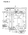
- FIG. 1 there is shown a block diagram of a first embodiment of the microprocessor in accordance with the present invention.
- the shown microprocessor includes a data controller 10 bidirectionally coupled to an external data bus 12 for interfacing between the inside of the microprocessor and the external data bus 12. For example, this external data bus 12 is directly coupled with an external memory 14.
- the microprocessor also includes an access controller 16 bidirectionally coupled to the external data bus 12.
- the access controller 16 outputs to the data controller 10 various information for accessing the external data bus 12. For example, the access controller 16 outputs a data access request signal REQ, 100 and a signal LENZ, 102 indicating that a remaining length of a block transfer is zero, to the data controller 10.
- the data controller 10 outputs to the access controller 16 a ready signal RDY, 104 indicating that it is ready for transferring data.
- the microprocessor includes an execution controller 18 for outputting a block transfer start signal BGN, 106 to the data controller 10.
- the data controller 10 When the block transfer operation has been completed, the data controller 10 generates an end signal FIN, 108 indicating that the block transfer operation has been completed. This end signal FIN, 108 is supplied to the access controller 16 and the execution controller 18.
- the data controller 10 also generates a signal CNT, 110 indicating the number of bytes of data that had been written into the external data bus 12 by the data controller 10.
- This signal CNT is applied to one input of an adder 20, which in turn has an output connected to a count register 22, which in turn has an output coupled to the other input of the adder 20, so that the count register 22 holds the total number of items of data that had been written into the external data bus 12 by the data controller 10.
- the output of the count register 22 is connected to the execution controller 18.
- the shown microprocessor also includes a decoder 24 coupled to receive an instruction through the external data bus 10 and to decode the received instruction for generating various control signals 112, 114, and 116 to the data controller 10, the access controller 16 and the execution controller 18.
- the data controller 10 internally includes a read operand register OPR coupled to the external data bus 12 so as to fetch data on the external data bus 12, and a write operand register OPW directly coupled to the read operand register OPR so as to directly receive data registered in the read operand register OPR.
- the write operand register OPW is coupled to the external data bus 12 so as to output the data registered in the write operand register OPW to the external data bus 12.
- the access controller 16 includes therein a transfer source length register SLEN and a transfer destination length register DLEN.
- the execution controller 18 internally includes a transfer source address holding register SR and a transfer destination address holding register DR.
- microprocessor itself and the shown functional units further include various elements which are well known to persons skilled in the art. However, those elements which do not have a direct relation with the present invention and therefore are not required in understanding the gist of the present invention, will not be shown for simplification of the drawings, and explanation thereof will be omitted for simplification of description.
- a transfer source address, a transfer source length, a transfer destination address and a transfer destination length are sent to and stored in the access controller 16 and the execution controller 104.
- the processing up to this condition is the same as that performed when a block transfer instruction is executed by only a microprogram.
- the access controller 16 checks whether or not the transfer source length and the transfer destination length are zero. If neither the transfer source length nor the transfer destination length is zero, and if the ready signal RDY, 104 is active to indicate that it is ready for transferring data, the access controller 16 decrements the transfer source length and the transfer destination length (respectively held in the transfer source length register SLEN and the transfer destination length register DLEN of the access controller 16) by only one, and activates the data access request signal REQ, 100 so as to cause data to be read from the external data bus 12.
- the data controller 10 fetches data which is outputted onto the external data bus 12 from a location of the memory 14 designated by an address counter or register not shown which indicates the transfer source address, and then stores the fetched data on the read operand register OPR. In this condition, the data controller 10 waits for the start signal BGN, 106 to be activated.
- the data controller 10 In response to the active start signal BGN, 106, the data controller 10 brings the operand read register OPR and the operand write register OPW into a condition in which the data held in the operand read register OPR is continuously transferred to the operand write register OPW without intermediary of the execution controller 18, so that the block transfer can be realized.
- the data controller 10 activates the ready signal RDY, 104 at each time that the read operand register OPR becomes empty and as soon as the read operand register OPR becomes empty, so that it is notified to the access controller 16 that it is ready for fetching next data. Namely, the data controller 10 waits the data access request signal REQ, 100 from the access controller 16 at each time that the read operand register OPR becomes empty. At this time, the data controller 10 also operates to transfer the data stored in the write operand register OPW to a location of the memory 14 designated by an address counter or register not shown indicating the transfer destination address.
- the access controller 16 decrements the transfer source address and the transfer destination length by only one, again, and on the other hand, the transfer source address and the transfer destination address of the not-shown address counters or registers are incremented so as to indicate addresses to be next read and written, respectively. At the same time, the access controller 16 activates the data access request signal REQ, 100, so that the above mentioned data transfer is repeated, again. Thus, the above mentioned operation is repeated until all of the data has been transferred.
- the data controller 10 activates the end signal FIN, 108 so as to inform the access controller 16 and the execution controller 18 that the block transfer has been completed.
- the block transfer of the data stored in the write operand register OPW of the data controller 10 to the memory is performed in units of bus cycle. Namely, assuming that the bus width of the external data bus 12 is four bytes, the block transfer is performed in units of four bytes.
- the data controller 10 In the course of execution of the block transfer, at each time that the data is written from the write operand register OPW to the external data bus 12, the data controller 10 outputs the number of effective bytes of written data as the signal CNT, 110. This signal CNT, 110 is added with the value of the count register 22 by the adder 20. Assuming that the bus width of the external data bus 12 is four bytes, the value indicated by the signal CNT, 110 is four in the way of the block transfer, but takes any value within a range of 1 to 3, dependently upon the transfer destination address and the transfer destination length, as regards the first transferred data and the last transferred data.
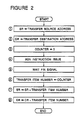
- the execution controller 18 of the shown embodiment does not perform the processing for the storing and the transfer of data, differently from the conventional microprocessor. Namely, the execution controller 18 controls the data controller 10 and manages and controls the transfer source address and the transfer destination address, by means of a microprogram having a processing flow shown in Figure 2. As illustrated in Figure 2, the block transfer is executed as follow:
- the first embodiment of the present invention is such that the transfer data is transferred from the read operand register OPR directly to the write operand register OPW and then to the external data bus without intermediary of the execution controller. Namely, it is possible to transfer the data in same units as the bus width.
- the block transfer instruction when executed, a large amount of data is transferred, and therefore, a number of clocks are required for the large amount of data transfer. If an interrupt request generated from a device external to the microprocessor is masked in the course of execution of the block transfer instruction which needs a number of clocks, a real time processing performance of the microprocessor will decrease. Therefore, it is a general practice that the block transfer can be interrupted in response to an interrupt request from an external device.
- the first embodiment is configured that the transfer source address holding register SR and the transfer destination address holding register DR (which respectively hold the transfer source address and the transfer destination address) are respectively modified by the number of bytes of the actually transferred data in accordance with a microprogram when execution of the block transfer instruction has been completed. These modified values of the transfer source address holding register SR and the transfer destination address holding register DR can be used as a transfer restarting address when the block transfer instruction interrupted in response to the interrupt request from the external device is restarted.
- a second embodiment described hereinafter has a function of interrupting the block transfer in response to the interrupt request from the external device.
- FIG 3 there is shown a block diagram of the second embodiment of the microprocessor in accordance with the present invention.
- elements corresponding to those shown in Figure 1 are given the same Reference Numerals, and explanation thereof will be omitted.
- the second embodiment additionally includes an interrupt request hold mechanism (composed of for example, a flag) 26 for receiving and holding an interrupt request from an external device, and an OR gate 28 having a first input connected to an output of the interrupt request hold mechanism 26 and a second input connected to receive the end signal FIN, 108.
- An output of the OR gate 28 is connected to the execution controller 18.
- the execution controller 18 outputs an interrupt request signal ABT, 118 to the data controller 10.
- the execution of the microprogram is stopped.
- the cancel of the stop of the execution of the microprogram is effected by only the end signal FIN, 108 which is generated when the block transfer has been completed.
- the cancel of the stop of the execution of the microprogram is effected by a logical sum between the end signal FIN, 108 and the output of the interrupt request hold mechanism 26.
- the microprogram used in the second embodiment has a microinstruction for discriminating whether the cancel of the stop of the execution of the microprogram is required by the end signal FIN, 108 from the data controller 10 or the interrupt request from the external device.
- the execution controller 18 If the cancel of the stop of the execution of the microprogram is required by the interrupt request from the external device, the execution controller 18 generates the interrupt request signal ABT, 118 to the data controller 10 in order to request the interrupt of the block transfer. Thereafter, the execution controller waits the end signal FIN, 108 indicating that the block transfer has been interrupted. At the time when the end signal FIN, 108 is generated, the content of the count register 22 has been settled. Therefore, similarly to the first embodiment, the transfer source address holding register SR and the transfer destination address holding register DR are respectively modified by the number of bytes of the actually transferred data in accordance with the microprogram.
- FIG. 4 there is shown a flow chart illustrating a processing executed in the microprocessor shown in Figure 3.
- the execution controller 18 controls the data controller 10 and manages and controls the transfer source address and the transfer destination address, by means of a microprogram as follow:
- the microprocessor in accordance with the present invention is characterized in that a data transfer portion of the all processing required for realizing the block transfer is executed by only the data controller without intermediary of the execution controller, differently from the conventional microprocessor in which the all processing required for realizing the block transfer is executed by only the microprogram. Therefore, the microprocessor in accordance with the present invention can execute the block transfer by utilizing the bus transfer capability of the microprocessor to a maximum extent.
- the interrupt function for interrupting the block transfer can be realized by adding a simple circuit.
Landscapes
- Engineering & Computer Science (AREA)
- Software Systems (AREA)
- Theoretical Computer Science (AREA)
- Physics & Mathematics (AREA)
- General Engineering & Computer Science (AREA)
- General Physics & Mathematics (AREA)
- Executing Machine-Instructions (AREA)
- Debugging And Monitoring (AREA)
- Microcomputers (AREA)
- Memory System (AREA)
- Information Transfer Systems (AREA)
- Computer And Data Communications (AREA)
Applications Claiming Priority (2)
| Application Number | Priority Date | Filing Date | Title |
|---|---|---|---|
| JP2070195A JPH03269659A (ja) | 1990-03-19 | 1990-03-19 | マイクロプロセッサ |
| JP70195/90 | 1990-03-19 |
Publications (2)
| Publication Number | Publication Date |
|---|---|
| EP0448058A2 true EP0448058A2 (fr) | 1991-09-25 |
| EP0448058A3 EP0448058A3 (fr) | 1992-12-30 |
Family
ID=13424494
Family Applications (1)
| Application Number | Title | Priority Date | Filing Date |
|---|---|---|---|
| EP19910104264 Withdrawn EP0448058A3 (fr) | 1990-03-19 | 1991-03-19 | Microprocesseur capable de transférer des données sans l'intermédiaire d'une unité d'exécution |
Country Status (4)
| Country | Link |
|---|---|
| US (1) | US5278968A (fr) |
| EP (1) | EP0448058A3 (fr) |
| JP (1) | JPH03269659A (fr) |
| KR (1) | KR940003696B1 (fr) |
Families Citing this family (5)
| Publication number | Priority date | Publication date | Assignee | Title |
|---|---|---|---|---|
| JP2718292B2 (ja) * | 1991-07-24 | 1998-02-25 | 日本電気株式会社 | マイクロプロセッサ |
| US5535333A (en) * | 1993-03-30 | 1996-07-09 | International Business Machines Corporation | Adapter for interleaving second data with first data already transferred between first device and second device without having to arbitrate for ownership of communications channel |
| US5603050A (en) * | 1995-03-03 | 1997-02-11 | Compaq Computer Corporation | Direct memory access controller having programmable timing |
| US7096297B2 (en) * | 2004-03-19 | 2006-08-22 | International Business Machines Corporation | System and method for delaying an interrupt request until corresponding data is provided to a destination device |
| US7817816B2 (en) * | 2005-08-17 | 2010-10-19 | Microsoft Corporation | Embedded interaction code enabled surface type identification |
Family Cites Families (6)
| Publication number | Priority date | Publication date | Assignee | Title |
|---|---|---|---|---|
| JPS5621240A (en) * | 1979-07-27 | 1981-02-27 | Hitachi Ltd | Information processor |
| JPS57161936A (en) * | 1981-03-31 | 1982-10-05 | Fujitsu Ltd | Microprgram controlled information processing device |
| JPS6057457A (ja) * | 1983-09-07 | 1985-04-03 | Ricoh Co Ltd | Dma装置 |
| US4797853A (en) * | 1985-11-15 | 1989-01-10 | Unisys Corporation | Direct memory access controller for improved system security, memory to memory transfers, and interrupt processing |
| EP0288649B1 (fr) * | 1987-04-22 | 1992-10-21 | International Business Machines Corporation | Système de commande de mémoire |
| EP0375883A3 (fr) * | 1988-12-30 | 1991-05-29 | International Business Machines Corporation | Système d'antémémoire |
-
1990
- 1990-03-19 JP JP2070195A patent/JPH03269659A/ja active Pending
-
1991
- 1991-03-19 EP EP19910104264 patent/EP0448058A3/fr not_active Withdrawn
- 1991-03-19 KR KR1019910004297A patent/KR940003696B1/ko not_active Expired - Fee Related
- 1991-03-19 US US07/672,527 patent/US5278968A/en not_active Expired - Fee Related
Also Published As
| Publication number | Publication date |
|---|---|
| US5278968A (en) | 1994-01-11 |
| EP0448058A3 (fr) | 1992-12-30 |
| JPH03269659A (ja) | 1991-12-02 |
| KR940003696B1 (ko) | 1994-04-27 |
| KR910017276A (ko) | 1991-11-05 |
Similar Documents
| Publication | Publication Date | Title |
|---|---|---|
| JP3644959B2 (ja) | マイクロプロセッサシステム | |
| US5481734A (en) | Data processor having 2n bits width data bus for context switching function | |
| US5440747A (en) | Data processor with control logic for storing operation mode status and associated method | |
| US5502827A (en) | Pipelined data processor for floating point and integer operation with exception handling | |
| US4847748A (en) | Virtual memory arrangement data processing system with decoding and execution of prefetched instructions in parallel | |
| KR970003321B1 (ko) | 코프로세서 지정 시스템 | |
| JPH05204709A (ja) | プロセッサ | |
| US5410721A (en) | System and method for incrementing a program counter | |
| US5410660A (en) | System and method for executing branch on bit set/clear instructions using microprogramming flow | |
| US20050172109A1 (en) | Register pointer trap | |
| US5278968A (en) | Microprocessor capable of transferring data without intermediating execution unit | |
| JPH06161779A (ja) | データ処理装置の割込み制御方式 | |
| EP0573071A2 (fr) | Microprocesseur | |
| JP2522048B2 (ja) | マイクロプロセッサ及びそれを使用したデ―タ処理装置 | |
| JP2696578B2 (ja) | データ処理装置 | |
| TW399176B (en) | Microprocessor access control unit upon fetching address queue | |
| JPH06131198A (ja) | データ処理装置 | |
| Execution et al. | Radiation Hardened Real Time Express™ Microcontroller | |
| JPH05113884A (ja) | 性能調整回路 |
Legal Events
| Date | Code | Title | Description |
|---|---|---|---|
| PUAI | Public reference made under article 153(3) epc to a published international application that has entered the european phase |
Free format text: ORIGINAL CODE: 0009012 |
|
| 17P | Request for examination filed |
Effective date: 19910412 |
|
| AK | Designated contracting states |
Kind code of ref document: A2 Designated state(s): DE FR GB |
|
| PUAL | Search report despatched |
Free format text: ORIGINAL CODE: 0009013 |
|
| AK | Designated contracting states |
Kind code of ref document: A3 Designated state(s): DE FR GB |
|
| 17Q | First examination report despatched |
Effective date: 19961122 |
|
| STAA | Information on the status of an ep patent application or granted ep patent |
Free format text: STATUS: THE APPLICATION HAS BEEN WITHDRAWN |
|
| 18W | Application withdrawn |
Withdrawal date: 19970306 |