EP0447917A2 - Charge transfer device - Google Patents
Charge transfer device Download PDFInfo
- Publication number
- EP0447917A2 EP0447917A2 EP91103715A EP91103715A EP0447917A2 EP 0447917 A2 EP0447917 A2 EP 0447917A2 EP 91103715 A EP91103715 A EP 91103715A EP 91103715 A EP91103715 A EP 91103715A EP 0447917 A2 EP0447917 A2 EP 0447917A2
- Authority
- EP
- European Patent Office
- Prior art keywords
- reset
- transistor
- voltage
- charge transfer
- gate
- Prior art date
- Legal status (The legal status is an assumption and is not a legal conclusion. Google has not performed a legal analysis and makes no representation as to the accuracy of the status listed.)
- Granted
Links
Images


Classifications
-
- G—PHYSICS
- G11—INFORMATION STORAGE
- G11C—STATIC STORES
- G11C19/00—Digital stores in which the information is moved stepwise, e.g. shift registers
- G11C19/28—Digital stores in which the information is moved stepwise, e.g. shift registers using semiconductor elements
- G11C19/282—Digital stores in which the information is moved stepwise, e.g. shift registers using semiconductor elements with charge storage in a depletion layer, i.e. charge coupled devices [CCD]
- G11C19/285—Peripheral circuits, e.g. for writing into the first stage; for reading-out of the last stage
-
- G—PHYSICS
- G11—INFORMATION STORAGE
- G11C—STATIC STORES
- G11C27/00—Electric analogue stores, e.g. for storing instantaneous values
- G11C27/04—Shift registers
Definitions
- charge transfer devices having a buried channel have comprised an output circuit requiring a high voltage for a reading of a transferred charge.
- most of the present systems are of a 5V voltage supply type, and therefore, have a pumping-up circuit for generating a high voltage and a DC clamp circuit receiving the generated high voltage for supplying a calibrated high voltage to the output circuit for the charge transfer device.
- the charge transfer devices inevitably have dispersion or variation in manufacture, for example, a potential of a channel under a reset gate also has dispersion or variation. In order to compensate the dispersion or variation of the channel potential, it has been necessary to make a complicated adjustment for a reset pulse voltage.
- a charge transfer device comprising: a charge transfer section having a charge transfer region formed in a semiconductor substrate and transfer electrodes formed on the semiconductor substrate; a reset transistor having a floating diffusion region formed in the semiconductor substrate for receiving an electric charge transferred from the charge transfer section, a reset drain applied with a reset voltage, and a reset gate formed above a channel between the floating diffusion region and the reset drain, the reset gate being applied with a reset pulse; potential detection means for detecting a potential of a channel of the reset transistor when the reset transistor is in a resetting operation; and voltage following means for causing the potential of the channel of the reset transistor when the reset transistor is in the resetting operation, to follow the reset voltage.
- the voltage following means operates to make the potential of the channel of the reset transistor when the reset transistor is in tile resetting operation, consistent with the reset voltage.
- the voltage following means can cause the reset voltage when the reset transistor is in the resetting operation, to follow the voltage detected by the potential detection means.
- the voltage following means operates to make the reset voltage when the reset transistor is in the resetting operation, consistent with the voltage detected by the potential detection means.
- FIG. 1A there is shown a diagrammatic sectional view of a conventional buried channel type charge transfer device.
- the charge transfer device includes a p-type semiconductor substrate 1 having an upper surface coated with an insulating layer 2.
- Transfer electrodes 2a, 2b and 2c and an output gate 3 are provided on the insulating layer 2.
- the transfer electrodes 2a, 2b and 2c are applied with a two-phase transfer clock, namely, are alternately applied with clocks ⁇ 1 and ⁇ 2 opposite to each other in phase, and the output gate 3 is connected to a fixed output gate voltage V OG .
- a floating diffusion 4 is formed at a surface region of the substrate 1 under the insulating layer 2 so as to convert a transferred signal charge into a potential change. Adjacent to the floating diffusion 4, a reset gate 5 is formed on the insulating layer 2.
- This reset gate 5 is connected to receive a reset pulse ⁇ R in synchronism with the transfer clock.
- a reset drain 6 is formed at the surface region of the substrate 1 under the insulating layer 2 and adjacent to the reset gate 5. This reset drain 6 is connected to a constant reset voltage V RD .
- the floating diffusion 4, the reset gate 5 and the reset drain 6 form a reset transistor of a MOS type.
- n-type diffusion layer 7 is formed at the surface region of the substrate so as to form a buried channel of the charge transfer section and a channel of the reset transistor, and a plurality of p-type barrier layers 8 are formed in the n-type diffusion layer 7.
- the amount of charge which can be converted into a voltage by the floating diffusion 4 is determined by a difference ⁇ V FD between the reset voltage V RD applied to the reset drain 6 and a potential ⁇ OG under the output gate 3 applied with the output gate voltage V OG .
- ⁇ V FD
- the value of ⁇ V FD is required to be not less than a certain constant value in order to ensure a required dynamic range.
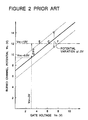
- a gate voltage and a buried channel potential have a relation as shown in Figure 2.
- the buried channel potential ⁇ G under the gate electrode is considerably higher than the gate electrode voltage V G .
- the reset voltage V RD is obtained by pumping up the voltage supply voltage to 12V.
- the reset pulse ⁇ R is obtained by a DC clamp circuit using a diode D as shown in Figure 3A. This clamp circuit operates to clamp a low level of an input pulse ⁇ R1 to a voltage V OFF determined by a voltage divider formed of resistors R1 and R2.
- the potential ⁇ G of the buried channel in relation to the gate voltage V G ordinarily has a manufacture dispersion or variation of ⁇ 1.5V. Therefore, the high level voltage of the reset pulse ⁇ R is required to be capable of being changed within a range from a point F to a point F in Figure 2, namely in the range of 4.5V to 8.0V. This means that the voltage V OFF in the DC clamp circuit shown in Figure 3A is required to be modified in order to compensate the manufacture dispersion or variation. For this purpose, it becomes necessary to adjust the resistance of the resistor R1 or R2 in the conventional circuit, which needs a very complicated adjustment.
- FIG 4 there is shown a circuit diagram of a first embodiment of the charge transfer device in accordance with the present invention.
- elements corresponding to those shown in Figure 1 are given the same Reference Numerals, and explanation thereof will be omitted.
- the shown charge transfer device has a ⁇ RH detection circuit 10 for detecting a potential ⁇ RH of a channel under a reset gate 5 when the reset pulse ⁇ R is at a high level, and a clamp circuit 11 including a comparator 14, a diode D1 having an anode connected to an output of the comparator 14, and a capacitor C1 having one end connected to a cathode of the diode D1.
- the shown charge transfer device also includes a ⁇ R peak hold circuit 12 composed of a diode D2 having an anode connected to the cathode of the diode D1 and a capacitor C2 having one end connected to an anode of the diode D2 and the other connected to ground.
- the ⁇ R peak hold circuit 12 operates to hold a high level of the reset pulse ⁇ R .
- Reference Numeral 13 designates an output circuit of a charge transfer device to be properly operated.
- the ⁇ RH detection circuit 10 includes a MOS transistor composed of a source region 41 and a drain region 61 formed in the p-type substrate 1, and an n-type diffusion region 7 formed between the source region 41 and the drain region 61.
- the insulating layer 2 covers the source region 41, the n-type diffusion region 7 and the drain region 61 formed in the p-type substrate 1.
- a gate electrode 51 is formed on the insulating layer 2 above the n-type diffusion region 7 formed between the source region 41 and the drain region 61.
- the MOS transistor of the ⁇ RH detection circuit 10 is a dummy transistor having the same characteristics in size, in voltage gain, in threshold and in others, as those of a MOS transistor (the reset transistor) formed of the floating diffusion 4, the reset gate 5 and the reset drain 6 in the charge transfer device output circuit 13.
- the drain 61 of the dummy transistor is connected to a high voltage V DD which is not less than the reset voltage V RD .
- the source 41 is grounded through a resistor R having a resistance which is several times of an on-resistance of the dummy transistor.
- the gate electrode 51 is connected to the cathode of the diode D2 of the ⁇ R peak hold circuit 12.
- an output voltage V4 of the comparator 14 rises.
- the rise of the output voltage V4 of the comparator 14 causes to raise a DC component of an output of V1 of the clamp circuit 11 which is a level shifted output of an input pulse ⁇ R1 .
- the output of V1 of the clamp circuit 11 is applied to the reset gate 5 as the reset pulse, and a peak value of the output V1 of the clamp circuit 11 is held in the ⁇ R peak hold circuit 12.
- the output voltage V2 of the ⁇ R peak hold circuit 12 is lower than the peak value of the clamp circuit output V1 by the forward direction voltage drop V F of the diode D2.
- the high level of the reset pulse ⁇ R is higher than a required minimum voltage by the forward direction voltage drop V F of the diode D2. Since this forward direction voltage V F of the diode D2 exists as a voltage margin, it is preferable. Thus, an ideal high level of the reset pulse ⁇ R can be set.
- the first embodiment shown in Figure 4 operates to automatically adjust the reset pulse ⁇ R to the effect that the potential ⁇ RH of the channel under the reset gate 5 is ceaselessly consistent with the reset voltage V RD (or slightly deeper than V RD ). Therefore, it is possible to avoid the disadvantage in which the channel potential ⁇ RH varies in relation to the same reset pulse ⁇ R . In addition, it is also possible to avoid a troublesome or complicated procedure of a resistance adjustment for the level adjustment of the reset pulse ⁇ R .
- FIG 7 there is shown a circuit diagram of a second embodiment of the charge transfer device in accordance with the present invention.
- elements corresponding to those shown in Figure 4 are given the same Reference Numerals, and a detail explanation thereof will be omitted.
- the second embodiment of the charge transfer device in accordance with the present invention includes the ⁇ RH detection circuit 10 for detecting the potential ⁇ RH of the channel under the reset gate 5 when the reset pulse ⁇ R is at the high level, the ⁇ R peak hold circuit 12 for holding the peak level of the reset pulse ⁇ R , and an output circuit 13 of the charge transfer device, similarly to the first embodiment.
- the second embodiment does not include the clamp circuit 12 provided in the first embodiment.
- the second embodiment is characterized in that the high level and the low level of the reset pulse ⁇ R are fixed, and the source 41 of the dummy transistor is directly connected to the reset drain 6 of the reset transistor and also grounded through a capacitor C3. Therefore, the second embodiment does not control the high level of the reset pulse ⁇ R .
- the second embodiment is configured to cause the drain voltage V RD to follow the potential ⁇ RH of the channel under the reset gate when the fixed high level of the reset pulse ⁇ R is applied.
- the ⁇ R peak hold circuit 12 holds a high level of the reset pulse ⁇ R , and outputs an output voltage V12, which is consistent with the high level of the reset pulse ⁇ R , if it is assumed that the forward direction voltage drop of the diode D2 is zero.
- the output voltage V12 is applied to the gate 51 of the dummy transistor.
- the channel potential of the dummy transistor becomes equal to the channel potential ⁇ RH of the reset transistor when the reset pulse ⁇ R is at the high level, similarly to the first embodiment. Therefore, this channel potential ⁇ RH is outputted from the dummy transistor in the form of the source voltage V11 of the dummy transistor and applied to the reset drain 6 of the reset transistor.
- the channel potential ⁇ RH at the time of resetting can be made consistent with the potential of the reset drain. Accordingly, it is possible to avoid a troublesome level adjustment of the reset pulse ⁇ R .
- the second embodiment has a circuit construction greatly simpler than that of the first embodiment.
- the above mentioned embodiments have been a buried channel type charge transfer device.
- the present invention can be applied to a surface channel type charge transfer device.
- the conduction type of the respective regions in the charge transfer devices can also be inverted, the present invention can also be applied.
- a buffer can be inserted between the source 41 of the dummy transistor and the reset drain of the reset transistor. In this modification, it is possible to suppress a potential variation occurring at the time of the resetting.
- the charge transfer circuit in accordance with the present invention is characterized in that the potential of the channel under the reset gate is detected so that a minimum reset pulse voltage or reset drain voltage required for completing the resetting of the reset transistor is automatically applied to the reset gate or the reset drain.
- the variation of the channel potential under the reset gate caused by the manufacture variation can be compensated, and therefore, the troublesome voltage adjustment procedure for the reset pulse can be omitted.
- the channel potential and the reset drain voltage can be made substantially equal, a voltage operation margin of the device itself can be consequentially enlarged.
Landscapes
- Solid State Image Pick-Up Elements (AREA)
Abstract
Description
- The present invention relates to a charge transfer device, and more specifically, to an output circuit for a charge transfer device including an electrically floating diffusion at a substrate surface.
- In general, charge transfer devices having a buried channel have comprised an output circuit requiring a high voltage for a reading of a transferred charge. On the other hand, most of the present systems are of a 5V voltage supply type, and therefore, have a pumping-up circuit for generating a high voltage and a DC clamp circuit receiving the generated high voltage for supplying a calibrated high voltage to the output circuit for the charge transfer device. However, since the charge transfer devices inevitably have dispersion or variation in manufacture, for example, a potential of a channel under a reset gate also has dispersion or variation. In order to compensate the dispersion or variation of the channel potential, it has been necessary to make a complicated adjustment for a reset pulse voltage.
- Accordingly, it is an object of the present invention to provide a charge transfer device which has overcome the above mentioned defect of the conventional one.
- Another object of the present invention is to provide a charge transfer device capable of automatically compensating the channel potential variation.
- The above and other objects of the present invention are achieved in accordance with the present invention by a charge transfer device comprising:
a charge transfer section having a charge transfer region formed in a semiconductor substrate and transfer electrodes formed on the semiconductor substrate;
a reset transistor having a floating diffusion region formed in the semiconductor substrate for receiving an electric charge transferred from the charge transfer section, a reset drain applied with a reset voltage, and a reset gate formed above a channel between the floating diffusion region and the reset drain, the reset gate being applied with a reset pulse;
potential detection means for detecting a potential of a channel of the reset transistor when the reset transistor is in a resetting operation; and
voltage following means for causing the potential of the channel of the reset transistor when the reset transistor is in the resetting operation, to follow the reset voltage. - Preferably, the voltage following means operates to make the potential of the channel of the reset transistor when the reset transistor is in tile resetting operation, consistent with the reset voltage.
- In place of causing the potential of the channel of the reset transistor to follow the reset voltage, the voltage following means can cause the reset voltage when the reset transistor is in the resetting operation, to follow the voltage detected by the potential detection means. Preferably, the voltage following means operates to make the reset voltage when the reset transistor is in the resetting operation, consistent with the voltage detected by the potential detection means.
- The above and other objects, features and advantages of the present invention will be apparent from the following description of preferred embodiments of the invention with reference to the accompanying drawings.
-
- Figure 1A is a diagrammatic sectional view of a conventional buried channel type charge transfer device;
- Figures 1B and 1C illustrate two different conditions of potential wells formed in the charge transfer device shown in Figure 1A;
- Figure 2 is a graph illustrating a relation between a gate voltage and a buried channel potential;
- Figure 3A is a circuit diagram of a DC clamp circuit for adjusting the reset pulse φR applied to the output circuit of the charge transfer device;
- Figure 3B is a timing chart illustrating an operation of the clamp circuit shown in Figure 3A;
- Figure 4 is a circuit diagram of one embodiment of the charge transfer device in accordance with the present invention;
- Figure 5 illustrates a potential well in the output circuit of the charge transfer device shown in Figure 4;
- Figure 6 is a timing chart illustrating an operation of the charge transfer device shown in Figure 4; and
- Figure 7 is a circuit diagram of another embodiment of the charge transfer device in accordance with the present invention.
- Referring to Figure 1A, there is shown a diagrammatic sectional view of a conventional buried channel type charge transfer device.
- In Figure 1A, the charge transfer device includes a p-
type semiconductor substrate 1 having an upper surface coated with aninsulating layer 2.Transfer electrodes output gate 3 are provided on theinsulating layer 2. Thetransfer electrodes output gate 3 is connected to a fixed output gate voltage VOG.A floating diffusion 4 is formed at a surface region of thesubstrate 1 under theinsulating layer 2 so as to convert a transferred signal charge into a potential change. Adjacent to thefloating diffusion 4, areset gate 5 is formed on the insulatinglayer 2. Thisreset gate 5 is connected to receive a reset pulse φR in synchronism with the transfer clock. In addition, areset drain 6 is formed at the surface region of thesubstrate 1 under theinsulating layer 2 and adjacent to thereset gate 5. Thisreset drain 6 is connected to a constant reset voltage VRD. Thefloating diffusion 4, thereset gate 5 and thereset drain 6 form a reset transistor of a MOS type. - An n-
type diffusion layer 7 is formed at the surface region of the substrate so as to form a buried channel of the charge transfer section and a channel of the reset transistor, and a plurality of p-type barrier layers 8 are formed in the n-type diffusion layer 7. - Operation of the charge transfer device will be explained with reference to Figures 1B and 1C which illustrate two different conditions of potential wells formed in the charge transfer device shown in Figure 1A.
- (1) When the clock φ₁ applied to the
transfer electrodes transfer electrodes 2b is at a low level, an electric charge flows as indicated by anarrow 201 and is accumulated at a region under an output side electrode of thetransfer electrodes 2a (Figure 1B). - (2) When the clock φ₁ applied to the
transfer electrodes transfer electrodes 2b is brought to the high level, the electric charge accumulated at the region under the output side electrode of thetransfer electrodes 2a flows into thefloating diffusion 4 through a channel region under theoutput gate 3 applied with the fixed-output gate voltage VOG, as indicated by an arrow 202 (Figure 1C). Thus, the signal charge is detected in the form of a voltage signal. - (3) When the clocks applied to the
transfer electrodes arrow 203 so that the signal charge is extracted out of thereset drain 6. - With repetition of the above process, signal charges which have been transferred to the output circuit are sequentially read out in the form of a signal voltage.
- In the above mentioned charge transfer device, the amount of charge which can be converted into a voltage by the
floating diffusion 4 is determined by a difference ΔVFD between the reset voltage VRD applied to thereset drain 6 and a potential ΨOG under theoutput gate 3 applied with the output gate voltage VOG. ΔVFD = | VRD - ΨOG |. The value of ΔVFD is required to be not less than a certain constant value in order to ensure a required dynamic range. - In the case of a buried channel, a gate voltage and a buried channel potential have a relation as shown in Figure 2. Namely, as seen from Figure 2, the buried channel potential ψG under the gate electrode is considerably higher than the gate electrode voltage VG. On the other hand, in order to ensure that the signal charge is smoothly transferred from a region under the
transfer electrodes 2a through a region under theoutput gate electrode 3, the potential of the region under theoutput gate 3 is required to be deeper than the potential whentransfer electrode 2a is at the low level (ψG = 7V). In ordinary cases, therefore, the output gate is applied with the output gate voltage of VOG = 3V, so that the potential of the region under theoutput gate 3 is brought into ψOG = 9.5V. - Accordingly, in order to ensure the dynamic range of ΔVFD = 2.5V, the reset voltage VRD must be set to as a high voltage as 12V, as seen from Figure 2. If it is set that VRD = 12V, the channel potential ψRH when the reset pulse φR is at the high level is at least required to be higher than VRD (namely, higher than the point C in Figure 2). Therefore, the high level of the reset pulse φR is required to have as a high potential as 6.5V.
- In comparison with the above mentioned voltage condition, most of ordinary systems are of a 5V voltage supply type, and therefore, the reset voltage VRD is obtained by pumping up the voltage supply voltage to 12V. The reset pulse φR is obtained by a DC clamp circuit using a diode D as shown in Figure 3A. This clamp circuit operates to clamp a low level of an input pulse φR1 to a voltage VOFF determined by a voltage divider formed of resistors R₁ and R₂. Precisely, as seen from Figure 3B which is a timing chart illustrating an operation of the clamp circuit shown in Figure 3A, since the low level of the input pulse φR1 becomes lower than VOFF by a forward direction voltage drop of the diode D, the low level of the reset pulse φR is level-shifted to (VOFF - VF) and the high level of the reset pulse φR is level-shifted to (5 + VOFF - VF)
- However, the potential ψG of the buried channel in relation to the gate voltage VG ordinarily has a manufacture dispersion or variation of ±1.5V. Therefore, the high level voltage of the reset pulse φR is required to be capable of being changed within a range from a point F to a point F in Figure 2, namely in the range of 4.5V to 8.0V. This means that the voltage VOFF in the DC clamp circuit shown in Figure 3A is required to be modified in order to compensate the manufacture dispersion or variation. For this purpose, it becomes necessary to adjust the resistance of the resistor R₁ or R₂ in the conventional circuit, which needs a very complicated adjustment.
- Referring to Figure 4, there is shown a circuit diagram of a first embodiment of the charge transfer device in accordance with the present invention. In Figure 4, elements corresponding to those shown in Figure 1 are given the same Reference Numerals, and explanation thereof will be omitted.
- The shown charge transfer device has a ψRH detection circuit 10 for detecting a potential ψRH of a channel under a
reset gate 5 when the reset pulse φR is at a high level, and aclamp circuit 11 including acomparator 14, a diode D₁ having an anode connected to an output of thecomparator 14, and a capacitor C₁ having one end connected to a cathode of the diode D1. Theclamp circuit 11 compares a channel potential ψRH with a reset voltage VRD so as to automatically control a high level of the reset pulse VRD for the purpose of realizing a relation of ψRH = VRD. The shown charge transfer device also includes a φRpeak hold circuit 12 composed of a diode D2 having an anode connected to the cathode of the diode D1 and a capacitor C2 having one end connected to an anode of the diode D2 and the other connected to ground. The φRpeak hold circuit 12 operates to hold a high level of the reset pulse φR.Reference Numeral 13 designates an output circuit of a charge transfer device to be properly operated. - The ψRH detection circuit 10 includes a MOS transistor composed of a
source region 41 and adrain region 61 formed in the p-type substrate 1, and an n-type diffusion region 7 formed between thesource region 41 and thedrain region 61. The insulatinglayer 2 covers thesource region 41, the n-type diffusion region 7 and thedrain region 61 formed in the p-type substrate 1. Agate electrode 51 is formed on the insulatinglayer 2 above the n-type diffusion region 7 formed between thesource region 41 and thedrain region 61. The MOS transistor of the ψRH detection circuit 10 is a dummy transistor having the same characteristics in size, in voltage gain, in threshold and in others, as those of a MOS transistor (the reset transistor) formed of the floatingdiffusion 4, thereset gate 5 and thereset drain 6 in the charge transferdevice output circuit 13. - The
drain 61 of the dummy transistor is connected to a high voltage VDD which is not less than the reset voltage VRD. On the other hand, thesource 41 is grounded through a resistor R having a resistance which is several times of an on-resistance of the dummy transistor. Thegate electrode 51 is connected to the cathode of the diode D2 of the φRpeak hold circuit 12. - An operation of the ψRH detection circuit 10 will be operated with reference to Figure 5 illustrating the potential well formed in the dummy transistor of the ψRH detection circuit 10.
- Neglecting the forward direction voltage drop VF of the diode D₂, the high level of the reset pulse φR is outputted as an output voltage V₂ of the φR
peak hold circuit 12 and applied to thegate 51. Therefore, the potential of a channel under thegate 51 becomes the same as the potential of the channel under thereset gate 5 when the reset pulse φR is at the high level. Under this situation, a source potential V₃ of the dummy transistor becomes equal to the potential ψRH of the channel under thegate 51, as shown in Figure 5. The reason for this that electrons flows into thesource 41 through the resistor R, but only a portion of the electrons flowed into the source exceeding the channel potential ψRH under thegate electrode 51 is absorbed into thedrain 61 applied with the voltage VDD. Therefore, the channel potential ψRH can be detected in the form of the source voltage V₃ (V₃ = ψRH), and the detected voltage is compared with the reset voltage VRD of the charge transferdevice output circuit 13 by thecomparator 14 of theclamp circuit 11. - Now, an operation of the
clamp circuit 11 will be explained with reference to Figure 6. - Assuming that VRD > V₃ at a time t₁, an output voltage V₄ of the
comparator 14 rises. As shown in Figure 6, the rise of the output voltage V₄ of thecomparator 14 causes to raise a DC component of an output of V₁ of theclamp circuit 11 which is a level shifted output of an input pulse φR1. The output of V₁ of theclamp circuit 11 is applied to thereset gate 5 as the reset pulse, and a peak value of the output V₁ of theclamp circuit 11 is held in the φRpeak hold circuit 12. Actually, the output voltage V₂ of the φRpeak hold circuit 12 is lower than the peak value of the clamp circuit output V₁ by the forward direction voltage drop VF of the diode D₂. Therefore, the rise of the output voltage V₄ of thecomparator 14 raises the output voltage V₂ of the φRpeak hold circuit 12. The rise of the output voltage V₂ of the φRpeak hold circuit 12 causes to raise the output voltage V₃ of the ψRH detection circuit 10. Finally, the above mentioned feedback loop operation is repeated until it becomes V₃ = VRD. - At a time t₂ when it becomes V₃ = VRD, the high level of the reset pulse φR is higher than a required minimum voltage by the forward direction voltage drop VF of the diode D₂. Since this forward direction voltage VF of the diode D₂ exists as a voltage margin, it is preferable. Thus, an ideal high level of the reset pulse φR can be set.
- As seen from the above, the first embodiment shown in Figure 4 operates to automatically adjust the reset pulse φR to the effect that the potential ψRH of the channel under the
reset gate 5 is ceaselessly consistent with the reset voltage VRD (or slightly deeper than VRD). Therefore, it is possible to avoid the disadvantage in which the channel potential ψRH varies in relation to the same reset pulse φR. In addition, it is also possible to avoid a troublesome or complicated procedure of a resistance adjustment for the level adjustment of the reset pulse φR. - Turning to Figure 7, there is shown a circuit diagram of a second embodiment of the charge transfer device in accordance with the present invention. In Figure 7, elements corresponding to those shown in Figure 4 are given the same Reference Numerals, and a detail explanation thereof will be omitted.
- The second embodiment of the charge transfer device in accordance with the present invention includes the ψRH detection circuit 10 for detecting the potential ψRH of the channel under the
reset gate 5 when the reset pulse φR is at the high level, the φRpeak hold circuit 12 for holding the peak level of the reset pulse φR, and anoutput circuit 13 of the charge transfer device, similarly to the first embodiment. However, The second embodiment does not include theclamp circuit 12 provided in the first embodiment. The second embodiment is characterized in that the high level and the low level of the reset pulse φR are fixed, and thesource 41 of the dummy transistor is directly connected to thereset drain 6 of the reset transistor and also grounded through a capacitor C₃. Therefore, the second embodiment does not control the high level of the reset pulse φR. As a substitution, the second embodiment is configured to cause the drain voltage VRD to follow the potential ψRH of the channel under the reset gate when the fixed high level of the reset pulse φR is applied. - Now, an operation of the second embodiment will be explained. Assuming that the reset pulse φR is supplied from an external device, the φR
peak hold circuit 12 holds a high level of the reset pulse φR, and outputs an output voltage V₁₂, which is consistent with the high level of the reset pulse φR, if it is assumed that the forward direction voltage drop of the diode D₂ is zero. The output voltage V₁₂ is applied to thegate 51 of the dummy transistor. As a result, the channel potential of the dummy transistor becomes equal to the channel potential ψRH of the reset transistor when the reset pulse φR is at the high level, similarly to the first embodiment. Therefore, this channel potential ψRH is outputted from the dummy transistor in the form of the source voltage V₁₁ of the dummy transistor and applied to thereset drain 6 of the reset transistor. - With the above mentioned arrangement, the channel potential ψRH at the time of resetting can be made consistent with the potential of the reset drain. Accordingly, it is possible to avoid a troublesome level adjustment of the reset pulse φR.
- As seen from the above, the second embodiment has a circuit construction greatly simpler than that of the first embodiment.
- The above mentioned embodiments have been a buried channel type charge transfer device. However, the present invention can be applied to a surface channel type charge transfer device. In addition, even if the conduction type of the respective regions in the charge transfer devices can also be inverted, the present invention can also be applied.
- In the second embodiment, a buffer can be inserted between the
source 41 of the dummy transistor and the reset drain of the reset transistor. In this modification, it is possible to suppress a potential variation occurring at the time of the resetting. - As seen from the above, the charge transfer circuit in accordance with the present invention is characterized in that the potential of the channel under the reset gate is detected so that a minimum reset pulse voltage or reset drain voltage required for completing the resetting of the reset transistor is automatically applied to the reset gate or the reset drain. With the feature, the variation of the channel potential under the reset gate caused by the manufacture variation can be compensated, and therefore, the troublesome voltage adjustment procedure for the reset pulse can be omitted.
- In addition, since the channel potential and the reset drain voltage can be made substantially equal, a voltage operation margin of the device itself can be consequentially enlarged.
- The invention has thus been shown and described with reference to the specific embodiments. However, it should be noted that the present invention is in no way limited to the details of the illustrated structures but changes and modifications may be made within the scope of the appended claims.
Claims (9)
- A charge transfer device comprising:
a charge transfer section having a charge transfer region formed in a semiconductor substrate and transfer electrodes formed on said semiconductor substrate;
a reset transistor having a floating diffusion region formed in said semiconductor substrate for receiving an electric charge transferred from said charge transfer section, a reset drain applied with a reset voltage, and a reset gate formed above a channel between said floating diffusion region and said reset drain, said reset gate being applied with a reset pulse;
potential detection means for detecting a potential of a channel of said reset transistor when said reset transistor is in a resetting operation; and
voltage following means for causing said potential of said channel of said reset transistor to follow said reset voltage when said reset transistor is in said resetting operation. - A charge transfer device claimed in Claim 1 further including a peak hold circuit connected to said reset gate of said reset transistor for hold a peak level of said reset voltage and wherein said potential detection means includes a dummy transistor having a drain connected to receive a voltage having an absolute value larger than that of said reset voltage, a source grounded through a resistor having a resistance which is considerably larger than an on-resistance of said dummy transistor itself, and a gate electrode connected to an output of said peak hold circuit, said dummy transistor having the same characteristics as that of said reset transistor.
- A charge transfer device claimed in Claim 2 wherein said peak hold circuit includes a diode having an anode connected to said reset gate of said reset transistor and a cathode connected to said gate of said dummy transistor, and a capacitor having one end connected to said cathode of said diode and the other end connected to ground.
- A charge transfer device claimed in Claim 1 further including a clamp circuit having a comparator having a first input connected to said drain of said dummy transistor and a second input connected to said reset drain of said reset transistor, a second diode having an anode connected to an output of said comparator and a cathode connected to said reset gate of said reset transistor.
- A charge transfer device claimed in Claim 1 wherein said voltage following means operates to make the potential of the channel of said reset transistor when said reset transistor is in the resetting operation, consistent with said reset voltage.
- A charge transfer device comprising:
a charge transfer section having a charge transfer region formed in a semiconductor substrate and transfer electrodes formed on said semiconductor substrate;
a reset transistor having a floating diffusion region formed in said semiconductor substrate for receiving an electric charge transferred from said charge transfer section, a reset drain applied with a reset voltage, and a reset gate formed above a channel between said floating diffusion region and said reset drain, said reset gate being applied with a reset pulse;
potential detection means for detecting a potential of a channel of said reset transistor when said reset transistor is in a resetting operation; and
voltage following means for causing said reset voltage to follow the voltage detected by said potential detection means when said reset transistor is in said resetting operation. - A charge transfer device claimed in Claim 6 further including a peak hold circuit connected to said reset gate of said reset transistor for hold a peak level of said reset voltage and wherein said potential detection means includes a dummy transistor having a drain connected to receive a voltage having an absolute value larger than that of said reset voltage, a source grounded through a resistor having a resistance which is considerably larger than an on-resistance of said dummy transistor itself, and a gate electrode connected to an output of said peak hold circuit, said dummy transistor has the same characteristics as that of said reset transistor, said drain of said dummy-transistor being directly connected to said reset drain of said reset transistor.
- A charge transfer device claimed in Claim 7 wherein said peak hold circuit includes a diode having an anode connected to said reset gate of said reset transistor and a cathode connected to said gate of said dummy transistor, and a capacitor having one end connected to said cathode of said diode and the other end connected to ground.
- A charge transfer device claimed in Claim 6 wherein said voltage following means operates to make said reset voltage when said reset transistor is in the resetting operation, consistent with the voltage detected by said potential detection means.
Applications Claiming Priority (2)
| Application Number | Priority Date | Filing Date | Title |
|---|---|---|---|
| JP58989/90 | 1990-03-10 | ||
| JP2058989A JP2707784B2 (en) | 1990-03-10 | 1990-03-10 | Charge transfer device |
Publications (3)
| Publication Number | Publication Date |
|---|---|
| EP0447917A2 true EP0447917A2 (en) | 1991-09-25 |
| EP0447917A3 EP0447917A3 (en) | 1992-01-08 |
| EP0447917B1 EP0447917B1 (en) | 1995-12-20 |
Family
ID=13100258
Family Applications (1)
| Application Number | Title | Priority Date | Filing Date |
|---|---|---|---|
| EP91103715A Expired - Lifetime EP0447917B1 (en) | 1990-03-10 | 1991-03-11 | Charge transfer device |
Country Status (4)
| Country | Link |
|---|---|
| US (1) | US5224134A (en) |
| EP (1) | EP0447917B1 (en) |
| JP (1) | JP2707784B2 (en) |
| DE (1) | DE69115527T2 (en) |
Families Citing this family (3)
| Publication number | Priority date | Publication date | Assignee | Title |
|---|---|---|---|---|
| JPH07105489B2 (en) * | 1993-05-27 | 1995-11-13 | 日本電気株式会社 | Charge transfer device |
| JP3031815B2 (en) * | 1994-04-01 | 2000-04-10 | シャープ株式会社 | Charge detection element, method of manufacturing the same, and charge transfer detection device |
| US6858917B1 (en) * | 2003-12-05 | 2005-02-22 | National Semiconductor Corporation | Metal oxide semiconductor (MOS) bandgap voltage reference circuit |
Citations (2)
| Publication number | Priority date | Publication date | Assignee | Title |
|---|---|---|---|---|
| EP0199387A1 (en) * | 1985-03-25 | 1986-10-29 | Koninklijke Philips Electronics N.V. | Charge transfer device |
| EP0292895A2 (en) * | 1987-05-21 | 1988-11-30 | Kabushiki Kaisha Toshiba | Charge transfer device |
Family Cites Families (3)
| Publication number | Priority date | Publication date | Assignee | Title |
|---|---|---|---|---|
| JPS61131854U (en) * | 1985-02-06 | 1986-08-18 | ||
| JP2672507B2 (en) * | 1987-05-21 | 1997-11-05 | 株式会社東芝 | Charge transfer element |
| JPH084137B2 (en) * | 1988-01-12 | 1996-01-17 | 日本電気株式会社 | Output circuit of charge transfer device |
-
1990
- 1990-03-10 JP JP2058989A patent/JP2707784B2/en not_active Expired - Lifetime
-
1991
- 1991-03-11 EP EP91103715A patent/EP0447917B1/en not_active Expired - Lifetime
- 1991-03-11 DE DE69115527T patent/DE69115527T2/en not_active Expired - Fee Related
- 1991-03-11 US US07/667,155 patent/US5224134A/en not_active Expired - Fee Related
Patent Citations (2)
| Publication number | Priority date | Publication date | Assignee | Title |
|---|---|---|---|---|
| EP0199387A1 (en) * | 1985-03-25 | 1986-10-29 | Koninklijke Philips Electronics N.V. | Charge transfer device |
| EP0292895A2 (en) * | 1987-05-21 | 1988-11-30 | Kabushiki Kaisha Toshiba | Charge transfer device |
Also Published As
| Publication number | Publication date |
|---|---|
| DE69115527T2 (en) | 1996-07-18 |
| JPH03261150A (en) | 1991-11-21 |
| JP2707784B2 (en) | 1998-02-04 |
| US5224134A (en) | 1993-06-29 |
| DE69115527D1 (en) | 1996-02-01 |
| EP0447917B1 (en) | 1995-12-20 |
| EP0447917A3 (en) | 1992-01-08 |
Similar Documents
| Publication | Publication Date | Title |
|---|---|---|
| US7110030B1 (en) | Solid state image pickup apparatus | |
| US5191398A (en) | Charge transfer device producing a noise-free output | |
| KR100272648B1 (en) | Charge transfer device | |
| US6600513B1 (en) | Charge transfer device | |
| EP0377959B1 (en) | A method of driving a charge detection circuit | |
| EP0447917B1 (en) | Charge transfer device | |
| KR100259032B1 (en) | Solid stage image pick-up device | |
| EP0280097B1 (en) | Charge transfer device with booster circuit | |
| JPS6233751B2 (en) | ||
| US7088393B1 (en) | Output-compensated buffers with source-follower input structure, methods of operating same, and image capture devices using same | |
| US4631739A (en) | High dynamic range charge amplifier | |
| JPS61224357A (en) | Electric charge transfer unit | |
| EP0311529B1 (en) | Image sensor having charge storage regions | |
| US6797935B2 (en) | Method of charging the photodiode element in active pixel arrays | |
| US5172399A (en) | Semiconductor charge transfer device including charge quantity detection | |
| KR910006247B1 (en) | Charge transfer device | |
| US5336910A (en) | Charge coupled device of high sensitivity and high integration | |
| US6191440B1 (en) | Charge transfer device with improved charge detection sensitivity | |
| US5612554A (en) | Charge detection device and driver thereof | |
| US6437378B1 (en) | Charge coupled devices including charge signal amplifiers therein | |
| US10924700B2 (en) | Global shutter imager device | |
| JP3302834B2 (en) | Charge transfer method and device | |
| US7109784B2 (en) | Gate bias circuit for MOS Charge Coupled Devices | |
| JP3173806B2 (en) | Driving method of charge detection circuit | |
| JP2006086757A (en) | Charge transfer device of solid state imaging device and driving method of charge transfer device of solid state imaging device |
Legal Events
| Date | Code | Title | Description |
|---|---|---|---|
| PUAI | Public reference made under article 153(3) epc to a published international application that has entered the european phase |
Free format text: ORIGINAL CODE: 0009012 |
|
| 17P | Request for examination filed |
Effective date: 19910311 |
|
| AK | Designated contracting states |
Kind code of ref document: A2 Designated state(s): DE FR GB NL |
|
| PUAL | Search report despatched |
Free format text: ORIGINAL CODE: 0009013 |
|
| AK | Designated contracting states |
Kind code of ref document: A3 Designated state(s): DE FR GB NL |
|
| 17Q | First examination report despatched |
Effective date: 19940914 |
|
| GRAA | (expected) grant |
Free format text: ORIGINAL CODE: 0009210 |
|
| AK | Designated contracting states |
Kind code of ref document: B1 Designated state(s): DE FR GB NL |
|
| REF | Corresponds to: |
Ref document number: 69115527 Country of ref document: DE Date of ref document: 19960201 |
|
| ET | Fr: translation filed | ||
| PLBE | No opposition filed within time limit |
Free format text: ORIGINAL CODE: 0009261 |
|
| STAA | Information on the status of an ep patent application or granted ep patent |
Free format text: STATUS: NO OPPOSITION FILED WITHIN TIME LIMIT |
|
| 26N | No opposition filed | ||
| PGFP | Annual fee paid to national office [announced via postgrant information from national office to epo] |
Ref country code: DE Payment date: 20010306 Year of fee payment: 11 |
|
| PGFP | Annual fee paid to national office [announced via postgrant information from national office to epo] |
Ref country code: GB Payment date: 20010307 Year of fee payment: 11 |
|
| PGFP | Annual fee paid to national office [announced via postgrant information from national office to epo] |
Ref country code: FR Payment date: 20010313 Year of fee payment: 11 |
|
| PGFP | Annual fee paid to national office [announced via postgrant information from national office to epo] |
Ref country code: NL Payment date: 20010330 Year of fee payment: 11 |
|
| REG | Reference to a national code |
Ref country code: GB Ref legal event code: IF02 |
|
| PG25 | Lapsed in a contracting state [announced via postgrant information from national office to epo] |
Ref country code: GB Free format text: LAPSE BECAUSE OF NON-PAYMENT OF DUE FEES Effective date: 20020311 |
|
| PG25 | Lapsed in a contracting state [announced via postgrant information from national office to epo] |
Ref country code: NL Free format text: LAPSE BECAUSE OF NON-PAYMENT OF DUE FEES Effective date: 20021001 Ref country code: DE Free format text: LAPSE BECAUSE OF NON-PAYMENT OF DUE FEES Effective date: 20021001 |
|
| GBPC | Gb: european patent ceased through non-payment of renewal fee |
Effective date: 20020311 |
|
| PG25 | Lapsed in a contracting state [announced via postgrant information from national office to epo] |
Ref country code: FR Free format text: LAPSE BECAUSE OF NON-PAYMENT OF DUE FEES Effective date: 20021129 |
|
| NLV4 | Nl: lapsed or anulled due to non-payment of the annual fee |
Effective date: 20021001 |
|
| REG | Reference to a national code |
Ref country code: FR Ref legal event code: ST |