EP0280097B1 - Charge transfer device with booster circuit - Google Patents
Charge transfer device with booster circuit Download PDFInfo
- Publication number
- EP0280097B1 EP0280097B1 EP88101709A EP88101709A EP0280097B1 EP 0280097 B1 EP0280097 B1 EP 0280097B1 EP 88101709 A EP88101709 A EP 88101709A EP 88101709 A EP88101709 A EP 88101709A EP 0280097 B1 EP0280097 B1 EP 0280097B1
- Authority
- EP
- European Patent Office
- Prior art keywords
- mos transistor
- type mos
- current path
- voltage
- enhancement type
- Prior art date
- Legal status (The legal status is an assumption and is not a legal conclusion. Google has not performed a legal analysis and makes no representation as to the accuracy of the status listed.)
- Expired - Lifetime
Links
- 238000009792 diffusion process Methods 0.000 claims description 39
- 238000000034 method Methods 0.000 claims description 32
- 239000013256 coordination polymer Substances 0.000 claims description 16
- 239000004065 semiconductor Substances 0.000 claims description 13
- 239000000758 substrate Substances 0.000 claims description 12
- 239000003990 capacitor Substances 0.000 claims description 11
- 238000010276 construction Methods 0.000 claims description 7
- 229920006395 saturated elastomer Polymers 0.000 claims description 4
- 230000015572 biosynthetic process Effects 0.000 claims 1
- 238000006243 chemical reaction Methods 0.000 claims 1
- 229910021420 polycrystalline silicon Inorganic materials 0.000 description 5
- 229920005591 polysilicon Polymers 0.000 description 5
- 150000002500 ions Chemical class 0.000 description 4
- 238000004519 manufacturing process Methods 0.000 description 4
- 238000010586 diagram Methods 0.000 description 3
- 230000000694 effects Effects 0.000 description 3
- 239000012535 impurity Substances 0.000 description 3
- AMHIJMKZPBMCKI-PKLGAXGESA-N ctds Chemical compound O[C@@H]1[C@@H](OS(O)(=O)=O)[C@@H]2O[C@H](COS(O)(=O)=O)[C@H]1O[C@H]([C@@H]([C@H]1OS(O)(=O)=O)OS(O)(=O)=O)O[C@H](CO)[C@H]1O[C@@H](O[C@@H]1CO)[C@H](OS(O)(=O)=O)[C@@H](OS(O)(=O)=O)[C@@H]1O[C@@H](O[C@@H]1CO)[C@H](OS(O)(=O)=O)[C@@H](OS(O)(=O)=O)[C@@H]1O[C@@H](O[C@@H]1CO)[C@H](OS(O)(=O)=O)[C@@H](OS(O)(=O)=O)[C@@H]1O[C@@H](O[C@@H]1CO)[C@H](OS(O)(=O)=O)[C@@H](OS(O)(=O)=O)[C@@H]1O[C@@H](O[C@@H]1CO)[C@H](OS(O)(=O)=O)[C@@H](OS(O)(=O)=O)[C@@H]1O2 AMHIJMKZPBMCKI-PKLGAXGESA-N 0.000 description 2
- 238000001514 detection method Methods 0.000 description 2
- 230000003321 amplification Effects 0.000 description 1
- 230000000295 complement effect Effects 0.000 description 1
- 238000006073 displacement reaction Methods 0.000 description 1
- 230000001788 irregular Effects 0.000 description 1
- 238000003199 nucleic acid amplification method Methods 0.000 description 1
- 239000008188 pellet Substances 0.000 description 1
- 239000007787 solid Substances 0.000 description 1
Images


Classifications
-
- H—ELECTRICITY
- H04—ELECTRIC COMMUNICATION TECHNIQUE
- H04N—PICTORIAL COMMUNICATION, e.g. TELEVISION
- H04N5/00—Details of television systems
- H04N5/30—Transforming light or analogous information into electric information
-
- G—PHYSICS
- G11—INFORMATION STORAGE
- G11C—STATIC STORES
- G11C27/00—Electric analogue stores, e.g. for storing instantaneous values
- G11C27/04—Shift registers
-
- G—PHYSICS
- G11—INFORMATION STORAGE
- G11C—STATIC STORES
- G11C19/00—Digital stores in which the information is moved stepwise, e.g. shift registers
- G11C19/28—Digital stores in which the information is moved stepwise, e.g. shift registers using semiconductor elements
- G11C19/282—Digital stores in which the information is moved stepwise, e.g. shift registers using semiconductor elements with charge storage in a depletion layer, i.e. charge coupled devices [CCD]
- G11C19/285—Peripheral circuits, e.g. for writing into the first stage; for reading-out of the last stage
-
- H—ELECTRICITY
- H01—ELECTRIC ELEMENTS
- H01L—SEMICONDUCTOR DEVICES NOT COVERED BY CLASS H10
- H01L29/00—Semiconductor devices adapted for rectifying, amplifying, oscillating or switching, or capacitors or resistors with at least one potential-jump barrier or surface barrier, e.g. PN junction depletion layer or carrier concentration layer; Details of semiconductor bodies or of electrodes thereof ; Multistep manufacturing processes therefor
- H01L29/66—Types of semiconductor device ; Multistep manufacturing processes therefor
- H01L29/68—Types of semiconductor device ; Multistep manufacturing processes therefor controllable by only the electric current supplied, or only the electric potential applied, to an electrode which does not carry the current to be rectified, amplified or switched
- H01L29/76—Unipolar devices, e.g. field effect transistors
Definitions
- the present invention relates to an output unit for a charge transfer device (hereinafter referred to as a "CTD”) and, more particularly, to a reference voltage generator for a voltage step-up circuit for applying a stepped-up voltage to a drain.
- CTD charge transfer device
- CTDs are widely used in solid state image sensors, charge transfer type delay lines, comb line filters, transversal filters, and so forth.
- a floating diffusion system is a known type of semiconductor integrated CTD signal output system.
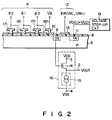
- One of a number of CTDs which employ a floating diffusion system with step-up circuit is disclosed in Figs. 4 and 5 of Japanese Patent Disclosure Sho 59-132668, invented by the inventor of the present invention, Mr. Imai. The construction and the operation of the CTD with the step-up circuit will be described with reference to Figs. 1 and 2.
- An analog signal is input through terminal 1 to input unit 7 of CTD shown in Figs. 1 and 2.
- Input unit 7 converts the input signal to a signal charge whose charge amount is corresponding to the level of the input signal, and also adds to this signal charge a predetermined DC bias charge.
- the resulting signal charge is then transferred toward floating diffusion region 9 by charge transfer unit 8.
- Charge transfer unit 8 comprises a front surface region of semiconductor substrate 5 and transfer electrodes 17i, 18i (i is 1 to n). Transfer electrodes 17i, 18i transfer the signal charges of semiconductor substrate 5 according to two clock pulses ⁇ 1, ⁇ 2.
- the transferred signal charges are fed under output gate electrode 10 to floating diffusion region 9.
- Reset voltage VGG higher than power source voltage VDD, is applied by step-up circuit 19 to drain region 11.
- FET 14 of output circuit 16 is connected at its gate to floating diffusion region 9, and a constant current flows from current source 15 to a current path. FET 14 converts the signal charge fed to floating diffusion region 9 to voltage signal, and outputs voltage signal VOUT.
- the CTD can increase the charge containing capacity of floating diffusion region 9 without increasing the capacity of floating diffusion region 9.
- VGG voltage VGG is also applied to the gate of FET 14.
- the gate voltage of FET 14 at signal detecting time is denoted by VG
- the voltage between the drain and the source is VDS
- the voltage between the gate and the source is VGS
- the threshold voltage of MOS transistor 14 is VTHE
- the source voltage (the voltage of output terminal 2) is VO
- VDS VDD - VO ...(1)
- VGS - VTHE VG - VO - VTHE ...(2) It is necessary to satisfy the following formula to saturate FET 14 at signal detection time.
- Step-up circuit 19 for applying voltage VGG higher than power source voltage VDD to drain region 11 will be described.
- Fig. 4 shows a step-up circuit disclosed in Fig. 7 of the Japanese Patent Disclosure.
- Step-up circuit 19 in Fig. 4 has reference voltage generator 20 including depletion type MOS transistors 21, 22; and step-up portion 30 including MOS transistor 31, MOS transistor 32 and capacitor 33.
- MOS transistors 21, 22 have the same conductivity type as that of MOS transistor (MOS transistor including regions 9, 11 and electrode 13) for forming reset means 12 of the CTD.
- VGG - (Qs/CFD) VFD ⁇ VDD + VTHE ...(6)
- the lower limit of voltage VGG must be larger than potential value PnL under the transfer electrode 18n. Therefore, the following equation (7) is satisfied.
- ⁇ VGG - (Qs/CFD) VFD ⁇ VDD + VTHE ...(7)
- Threshold value VTHD of the depletion transistor and threshold value VTHE of the enhancement transistor are independently varied by process variations, e.g., the thickness of insulating film 6 in Fig. 2, the irregularity of ion density of ions to be implanted, the depth of the layer of implanted ions, and the irregular gate of the impurity density of the semiconductor substrate.
- reference voltage generator 20 in Fig. 4 is composed of the same conductivity type MOS transistors, output voltage VGG is constant irrespective of the process variations.
- is, for example, large, the tolerance of the lower limit of VFD is small from equation (7), and when VTHE is small, the tolerance of the upper limit of the VFD is mall from equation (7).
- an object of the present invention is to provide a charge transfer device with a voltage step-up circuit which does not reduce the margin of a range of a signal voltage of in a floating diffusion region due to a process variation and can provide good linearity and S/N at a predetermined power source voltage to produce an output signal of wide dynamic range.
- Another object of the present invention is to provide an output unit for a charge transfer device with a voltage step-up circuit which can produce an output signal of a predetermined level with good linearity and S/N at a low power source voltage.
- a charge transfer device comprising: a charge transfer unit (8) receiving predetermined clock signals ( ⁇ 1, ⁇ 2) for transferring a charge in a semiconductor substrate (5); a floating diffusion region (9) formed in the semiconductor substrate (5) for transferring a charge from the charge transfer unit (8); a drain region (11) formed separately from the floating diffusion region (9) in the semiconductor substrate (5); a reset electrode (13) formed over a region between the floating diffusion region (9) and the drain region (11) to receive a reset signal for controlling the conduction and nonconduction between the regions; voltage step-up circuit (19) having reference voltage generating circuit (40) receiving a predetermined voltage (VDD) for generating a reference voltage (VREF); and step-up circuit (32 to 34) receiving the reference voltage (VREF), adding a voltage to the reference voltage (VREF), and applying a voltage (VGG) raised to as high as the predetermined voltage (VDD) to the drain region (11); an output circuit (16) electrically connected to the floating diffusion region (9) for a clock signals ( ⁇ 1, ⁇
- the output voltage (VREF) of the reference voltage generator follows to the process variation. Therefore, the output (VGG) of the voltage step-up circuit 19 also follows the process variation.
- the dynamic range of the output signal of the charge transfer device can be maintained constant irrespective of a certain degree of process variation.
- the merits can be sufficiently provided by using the voltage step-up circuit to obtain a large dynamic range, good linearity and high S/N.
- the feature of the embodiment resides in that voltage VGG is varied in response to the degree of variation in threshold values VTHD , VTHE in the equation (7).
- the output voltage of the reference voltage source of the voltage step-up circuit depends upon the process variation.
- the voltage step-up circuit of embodiments of the present invention will be described with reference to Figs. 1, 2 and 5.
- Fig. 5 shows a voltage step-up circuit according to an embodiment of the present invention.
- the voltage step-up circuit of Fig. 5 comprises reference voltage generator 40 and step-up portion 50.
- Reference voltage generator 40 comprises depletion type (D type) MOS transistor 41 connected at its drain to a VDD power source node, and connected at its source and gate to reference voltage output terminal 43; and enhancement type (E type) MOS transistor 42 connected at its source to VSS power source node and connected at its drain and gate to reference voltage output terminal 43.
- enhancement type (E type) MOS transistor 42 connected at its source to VSS power source node and connected at its drain and gate to reference voltage output terminal 43.
- Step-up portion 50 comprises first E type MOS transistor 51 connected at one end of a current path to reference voltage output terminal 43 for applying clock pulse CP to its gate; capacitor 52 connected at its one end to the other end of the current path of first E type MOS transistor 51 for applying clock pulse CP to its other end; and second E type MOS transistor 54 connected at its one end of the current path to the connecting node 53 of first E type MOS transistor 51 and capacitor 52 for applying clock pulse CP ⁇ to its gate to generate output voltage VGG of a voltage step-up circuit 19 to other end 55 of the current path.
- Clock pulse CP ⁇ has the same phase as clock pulse CP, and has a high level which is higher by voltage level corresponding to threshold value VTHE of MOS transistor 54 than the high level of the clock pulse generated at node 53.
- D type MOS transistor 41 has the same conductivity type and the same construction as a MOS transistor (having regions 9, 11, and electrode 13 of Fig. 2) for forming CTD reset circuit (12 in Fig. 1).
- D type MOS transistor 41 is manufactured in the same process as a MOS transistor for forming reset circuit 12, and is saturated.
- E type MOS transistor 42 has the same conductivity type (N type in Fig. 2) as MOS transistor (14 in Fig. 2) connected at its gate to the floating diffusion region (9 in Fig. 2) of CTD, and is saturated.
- VTHE 1V
- VTHD -6V
- 0.2
- VTHE 1 ⁇ 0.4V
- VTHD -6 ⁇ 1V due to the process variation.
- reference voltage VREF varies in response to the variation in the threshold voltages of transistors 41, 42 due to process variation.
- the variation in reference voltage output (process dependency) reflects output voltage VGG of voltage step-up circuit 19.
- VGG becomes high. Therefore, as understood from the equation (7), bias voltage VFD of signal in floating diffusion region 9 becomes high, and both upper and lower limits of the equation (7) are shifted to higher positions.
- the tolerance of the operating range of the signal charge is increased as compared with the case that reference voltage VREF is fixed.
- VGG becomes low. Therefore, as understood from the equation (7), bias voltage VFD of signal in floating diffusion region 9 becomes low, and both upper and lower limits of the equation (7) are shifted to lower positions.
- the voltage step-up circuit of the invention is not limited to the construction in Fig. 5.
- step-up portion 30 in Fig. 4 may be used instead of step-up portion 50 in Fig. 5.
- the output voltage of voltage step-up circuit 19 is reduced by the threshold voltage of MOS diode 32 as compared with output voltage VGG of the voltage step-up circuit of Fig. 5 by the operation of MOS diode 32. Therefore, it is necessary to set the reference voltage higher by threshold value VTHE (1V in the above example) of MOS diode 32 in Fig. 4 than the reference voltage of Fig. 5 under process center conditions. Thus, values of MOS transistors 41, 42 are altered.
- MOS transistors 31, 51 may be replaced by depletion type MOS transistors or MOS diodes.
- Transistors 32, 54 may be replaced by depletion type MOS transistors. When the depletion type MOS transistors are used, it is necessary to apply a clock pulse of the voltage relation that the transistors are completely turned OFF when a low level clock is applied to the gates and transistors are completely turned ON when a high level clock is applied.
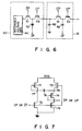
- a voltage step-up circuit in Fig. 6 may also be employed.
- the voltage step-up circuit in Fig. 6 the voltage step-up circuit in Fig. 5 is connected in a cascade, the input terminal of second stage voltage step-up circuit 61 is connected to the output terminal of the first stage voltage step-up circuit 60, and the reference voltage generator is replaced with a capacitor 62.
- normal clock pulses CP, CP and CP ⁇ (which has stepped-up high level) are supplied to the first stage voltage step-up circuit 60.
- clock pulse CP ⁇ and CP ⁇ which have been stepped-up to a high level are applied.
- Clock pulses CP ⁇ and CP ⁇ are, for example, obtained by voltage step-up circuit 70 having transistors 71 to 75, and capacitor 76 in Fig. 7.
- clock pulse CP or CP when clock pulse CP or CP is high level, node 77 is low level, and transistors 73, 75 are turned ON. Capacitor 76 is charged, and voltage of one terminal 78 of capacitor 76 becomes VDD. At this time, CP ⁇ or CP ⁇ becomes low level (substantially ground level).
- clock pulse CP or CP is low level, node 77 is high level, and transistors 73, 75 are turned OFF.
- the voltage of one terminal 78 of capacitor 76 becomes 2VDD(VDD+VDD), and this voltage become CP ⁇ or CP ⁇ .
- Clock pulse CP ⁇ varies from 0V to 3VDD at level synchronously with clock pulse CP and obtained by a circuit similar to Fig. 7.
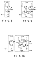
- Reference voltage generator 80 in Fig. 8 comprises a D type MOS transistor 81 connected at its drain and gate to the VDD power source node, and connected at a source to reference voltage output terminal 83 for operating in a nonsaturated state; and an E type MOS transistor 82 connected at its source to the VSS voltage source, and connected at its gate and source to reference voltage output terminal 83.
- reference voltage VREF follows the process variation in the same manner as the case that reference voltage generator 40 of Fig. 5 is used.
- the drain and the gate of E type MOS transistor 91 are connected to VDD power source node, and the gate and the source of D type MOS transistor 92 are connected to VSS voltage source.
- the gate of E-type transistor 42 in reference voltage generator circuit 40 in Fig. 5 is switching connected from a reference voltage output terminal to junction 93 between transistors 91 and 92.
- Transistors 41 and 42 have their junction taken out as reference output voltage terminal 94.
- E type MOS transistor 91 and D type MOS transistor 92 have greater VTHE and
- E type MOS transistor 91 and D type MOS transistor 92 have smaller VTHE and
- reference voltage generator circuit 90 has a much better process tracing characteristic than that of reference voltage generator circuit 40. It is to be noted that the same effect is also obtained even if the gate of D type MOS transistor 41 in Fig. 9 is connected to VDD power source node instead.
- Fig. 10 shows a reference voltage generator of such a type as used as reference voltage generator 40 in Fig. 5 and as reference voltage generator of Fig. 9.
- the gate of D type MOS transistor 41 in circuit 90 is switching connected from output terminal 94 to reference voltage output terminal 43.
- of D type MOS transistor 41 and VTHE of E type MOS transistor 42 are large, gate voltage VG2 becomes large. Therefore, trans-conductance gm of D type MOS transistor 41 of reference voltage generator 90 is increased in the amount that
- of D type MOS transistor 41 of circuit 40 is small and VTHE of E type MOS transistor 42 is small, gate voltage VG2 is reduced.
- reference voltage generator 80 of Fig. 8 or reference voltage generator 90 of Fig. 9 may be used instead of circuit 40.
- a plurality of circuits 90 are provided and may be connected in cascade so that the output voltages of the front stage circuits are connected to the input of the rear stage circuits.
- D type MOS transistor for forming the reference voltage generator of the same process as the transistor for forming a reset circuit 12 to perform the process followability of the reference voltage generator.
- D type MOS transistors are manufactured in the same process and E type MOS transistors are manufactured in the same process, because the process variation affects the transistors in an equal ratio.
- floating diffusion region 9, drain region 11, and source region 411 and drain region 412 of transistor 41 are formed by thermal diffusion in semiconductor substrate 5.
- Impurity ions X are implanted under the same conditions to a region between regions 9 and 11 and channel region between source region 411 and drain region 412.
- insulating film 6 is formed on semiconductor substrate 5.
- Polysilicon layer (so-called first polysilicon layer) is formed on insulating film 6.
- First polysilicon layer is patterned, and as shown in Fig. 11C, reset electrode 13 and gate electrode 413 of transistor 41 are formed together with transfer electrode 18i.
- insulating layer 110 is formed. An opening for forming electrode 17i is formed on insulating layer 110.
- Polysilicon layer (so-called second polysilicon layer) is formed on insulating layer 110, and patterned to form transfer electrode 17i, and output gate electrode 10 as shown in Fig. 11E.
- D type MOS transistor 41 and MOS transistor for forming reset circuit 12 are formed in the same steps and have the same constitution. Therefore, the variations in the thicknesses of the insulating films, electrode forming conditions, variations in the impurity densities in substrates, channel regions, semiconductor layers equally affect both the transistors to complete the process followability. In other words, when the transistors are formed as described above, the ratio of displacement from the process center of the process in a certain pellet equally affect the elements on the wafer, thereby accomplishing the desired effects.
- the above manufacturing steps are by way of example only, and the manufacturing steps are not limited to the embodiment.
- the voltage step-up circuit is provided. Therefore, the output signal of large level having good linearity and high S/N can be obtained under predetermined power source voltage. Or, the power source voltage necessary to obtain the output signal of a predetermined level having good linearity and high S/N can be reduced.
- the reference voltage generator of the voltage step-up circuit is deviced to provide process followability at the reference voltage output. Therefore, the output voltage of the voltage step-up circuit has the process followability. As a result, even if certain process variation occurs, the dynamic range of the output signal of CTD is widely maintained to obtain the output signal having good linearity and high S/N.
- the circuit formed of N-channel MOS transistors has been described as an example.
- the present invention is not limited to the particular embodiments, but can be similarly applied to the case that P-channel MOS transistors or complementary MOS transistors are employed in the circuit.
Description
- The present invention relates to an output unit for a charge transfer device (hereinafter referred to as a "CTD") and, more particularly, to a reference voltage generator for a voltage step-up circuit for applying a stepped-up voltage to a drain.
- CTDs are widely used in solid state image sensors, charge transfer type delay lines, comb line filters, transversal filters, and so forth. A floating diffusion system is a known type of semiconductor integrated CTD signal output system. One of a number of CTDs which employ a floating diffusion system with step-up circuit is disclosed in Figs. 4 and 5 of Japanese Patent Disclosure Sho 59-132668, invented by the inventor of the present invention, Mr. Imai. The construction and the operation of the CTD with the step-up circuit will be described with reference to Figs. 1 and 2.
- An analog signal is input through terminal 1 to
input unit 7 of CTD shown in Figs. 1 and 2.Input unit 7 converts the input signal to a signal charge whose charge amount is corresponding to the level of the input signal, and also adds to this signal charge a predetermined DC bias charge. The resulting signal charge is then transferred toward floatingdiffusion region 9 bycharge transfer unit 8.Charge transfer unit 8 comprises a front surface region ofsemiconductor substrate 5 andtransfer electrodes Transfer electrodes semiconductor substrate 5 according to two clock pulses φ1, φ2. The transferred signal charges are fed underoutput gate electrode 10 to floatingdiffusion region 9. Reset voltage VGG, higher than power source voltage VDD, is applied by step-upcircuit 19 to drainregion 11. When reset pulse φR applied toreset gate electrode 13 is low voltage VRL, potential value PRL underreset gate electrode 13 becomes a value for electrically interruptingdrain region 11 and floatingdiffusion region 9 as shown in Fig. 3A. When reset pulse φR becomes high voltage VRH, potential value PRH underreset gate electrode 13 becomes a value for conducting floatingdiffusion region 9 anddrain region 11. The charge offloating diffusion region 9 is discharged (absorbed) underreset gate electrode 13 to drainregion 11, andfloating diffusion region 9 is reset to voltage VGG. When reset pulse φR again becomes low voltage VRL, floatingdiffusion region 9 becomes a floating state to wait for the next charge input. -
FET 14 ofoutput circuit 16 is connected at its gate to floatingdiffusion region 9, and a constant current flows fromcurrent source 15 to a current path.FET 14 converts the signal charge fed to floatingdiffusion region 9 to voltage signal, and outputs voltage signal VOUT. The dynamic range of output signal VOUT is proportional to the difference (PD-PG) = DR between potential PD and potential PG underoutput gate electrode 10. Therefore, when applied voltage VB ofoutput gate electrode 10 is set to the allowable value as low as possible with respect to potential PnL undertransfer electrode 18n of the final stage, the dynamic range of the output signal of the CTD in Figs. 1 and 2 becomes considerably larger than that of the output signal of the CTD applied with power source voltage VDD to drainregion 11 since voltage VGG is higher than power source voltage VDD. The CTD can increase the charge containing capacity of floatingdiffusion region 9 without increasing the capacity of floatingdiffusion region 9. - When
floating diffusion region 9 is reset, voltage VGG is also applied to the gate ofFET 14. When the gate voltage ofFET 14 at signal detecting time is denoted by VG, the voltage between the drain and the source is VDS, the voltage between the gate and the source is VGS, the threshold voltage ofMOS transistor 14 is VTHE and the source voltage (the voltage of output terminal 2) is VO, the following equations (1) and (2) are satisfied.


It is necessary to satisfy the following formula to saturateFET 14 at signal detection time.

- When the equations (1) and (2) are substituted for the formula (3), the following formula (4) is satisfied.

Therefore, when an output voltage having good linearity is required, it is necessary to determine the voltage relation so as to satisfy the above formula (4) at the signal detection time. - Then, step-up
circuit 19 for applying voltage VGG higher than power source voltage VDD to drainregion 11 will be described. Fig. 4 shows a step-up circuit disclosed in Fig. 7 of the Japanese Patent Disclosure. Step-upcircuit 19 in Fig. 4 hasreference voltage generator 20 including depletiontype MOS transistors 21, 22; and step-upportion 30 includingMOS transistor 31,MOS transistor 32 andcapacitor 33.MOS transistors 21, 22 have the same conductivity type as that of MOS transistor (MOStransistor including regions - In Fig. 4, when clock pulse CP is a low level and clock pulse
CP is a high level,MOS transistor 31 is turned on,MOS transistor 32 is turned off,capacitor 33 is charged, and the voltage acrosscapacitor 33 becomes VREF (the output voltage of node 23). When clock pulse CP then becomes high level,MOS transistor 31 is turned off,second MOS transistor 32 is turned on, and the output voltage ofnode 34 is raised by "the peak value of clock pulse CP minus threshold value VTH ofMOS transistor 32" higher than voltage VREF. - However, when
reference voltage generator 20 in Fig. 4 is used as a reference voltage generator of drain step-upcircuit 19 of the CTD, the following drawbacks occur. The higher output voltage VGG rises in the CTD in Figs. 1 and 2, the wider dynamic range DR shown in Fig. 3B becomes. When the potential ofdrain region 11 becomes higher than potential PRH underreset gate electrode 13 as a pulse of High level is applied to resetgate electrode 13, it is necessary to raise reset pulse φR. When bias voltage VFD of the signal atfloating diffusion region 9 is set to as high as VDD+VTHE,transistor 14 of signal processor (output circuit) 16 enters nonsaturated state to lose the linearity of the output signal. Therefore, the upper limit of the step-up level coincides with the maximum value for maintaining the linearity indicated by formula (4). When formula (4) is transformed, the following formula (4ʹ) is obtained

- Since VG=VFD exists, the following formula (4ʺ) is satisfied

- When the capacity of
floating diffusion region 9 is indicated by CFD and charge transferred to the floating diffusion region is indicated by Qs, the following equation (5) is satisfied.

- Qs/CFD corresponds to the voltage component of the signal charge of
floating diffusion region 9. Therefore, the following equation (6) is satisfied.

The lower limit of voltage VGG must be larger than potential value PnL under thetransfer electrode 18n. Therefore, the following equation (7) is satisfied.

The VTHD is the threshold value of the D-type MOS transistor formed ofregions electrode 13, and VTHD = PnL = approx. PG. - Threshold value VTHD of the depletion transistor and threshold value VTHE of the enhancement transistor are independently varied by process variations, e.g., the thickness of
insulating film 6 in Fig. 2, the irregularity of ion density of ions to be implanted, the depth of the layer of implanted ions, and the irregular gate of the impurity density of the semiconductor substrate. However, sincereference voltage generator 20 in Fig. 4 is composed of the same conductivity type MOS transistors, output voltage VGG is constant irrespective of the process variations. Thus, when | VTHD | is, for example, large, the tolerance of the lower limit of VFD is small from equation (7), and when VTHE is small, the tolerance of the upper limit of the VFD is mall from equation (7). - In Fig. 3B, voltage VGG (which does not alter by the process variation) is applied to the drain region, potential PD is constant. When insulating
film 6 is, for example, thickened, potential PG (=approx. PnL) is deepened, and dynamic range DR is reduced. Thus, the conventional art has such a disadvantage that CTD characteristic is altered due to the process variation. - Accordingly, an object of the present invention is to provide a charge transfer device with a voltage step-up circuit which does not reduce the margin of a range of a signal voltage of in a floating diffusion region due to a process variation and can provide good linearity and S/N at a predetermined power source voltage to produce an output signal of wide dynamic range.
- Another object of the present invention is to provide an output unit for a charge transfer device with a voltage step-up circuit which can produce an output signal of a predetermined level with good linearity and S/N at a low power source voltage.
- According to the present invention, there is provided a charge transfer device comprising:
a charge transfer unit (8) receiving predetermined clock signals (φ1, φ2) for transferring a charge in a semiconductor substrate (5);
a floating diffusion region (9) formed in the semiconductor substrate (5) for transferring a charge from the charge transfer unit (8);
a drain region (11) formed separately from the floating diffusion region (9) in the semiconductor substrate (5);
a reset electrode (13) formed over a region between the floating diffusion region (9) and the drain region (11) to receive a reset signal for controlling the conduction and nonconduction between the regions;
voltage step-up circuit (19) having reference voltage generating circuit (40) receiving a predetermined voltage (VDD) for generating a reference voltage (VREF); and step-up circuit (32 to 34) receiving the reference voltage (VREF), adding a voltage to the reference voltage (VREF), and applying a voltage (VGG) raised to as high as the predetermined voltage (VDD) to the drain region (11);
an output circuit (16) electrically connected to the floating diffusion region (9) for converting and outputting the charge stored in the floating diffusion region (9) to a signal having a voltage level substantially proportional to the charge amount;
said reference voltage generator (4) comprising:
a depletion type MOS transistor of the same conductivity type and substantially the same construction as MOS transistor formed of the reset electrode (13), the floating diffusion region (9) and the drain region (11); and
an enhancement type MOS transistor connected in cascade fashion with the depletion type MOS transistor (41). - With the construction described above, in the output unit of the charge transfer device according to the present invention, the output voltage (VREF) of the reference voltage generator follows to the process variation. Therefore, the output (VGG) of the voltage step-up
circuit 19 also follows the process variation. As understood from the equation (7), the dynamic range of the output signal of the charge transfer device can be maintained constant irrespective of a certain degree of process variation. The merits can be sufficiently provided by using the voltage step-up circuit to obtain a large dynamic range, good linearity and high S/N. - This invention can be more fully understood from the following detailed description when taken in conjunction with the accompanying drawings, in which:
- Figs. 1 to 4 are views for describing a conventional charge transfer device;
- Figs. 5 and 6 are circuit diagrams of a voltage step-up circuit of a charge transfer device according to embodiments of the present invention;
- Fig. 7 is a circuit diagram showing an example of a circuit for supplying clock pulses stepped up to a higher voltage to the circuit of Fig. 6;
- Figs. 8 to 10 are circuit diagrams showing another construction of a reference voltage generator used for the voltage step-up circuit; and
- Figs. 11A to 11E show manufacturing steps of a charge transfer device according to an embodiment of the present invention.
- The feature of the embodiment resides in that voltage VGG is varied in response to the degree of variation in threshold values VTHD , VTHE in the equation (7). To this end, the output voltage of the reference voltage source of the voltage step-up circuit depends upon the process variation. The voltage step-up circuit of embodiments of the present invention will be described with reference to Figs. 1, 2 and 5.
- Fig. 5 shows a voltage step-up circuit according to an embodiment of the present invention. The voltage step-up circuit of Fig. 5 comprises
reference voltage generator 40 and step-upportion 50.Reference voltage generator 40 comprises depletion type (D type)MOS transistor 41 connected at its drain to a VDD power source node, and connected at its source and gate to referencevoltage output terminal 43; and enhancement type (E type)MOS transistor 42 connected at its source to VSS power source node and connected at its drain and gate to referencevoltage output terminal 43. Step-upportion 50 comprises first Etype MOS transistor 51 connected at one end of a current path to referencevoltage output terminal 43 for applying clock pulseCP to its gate;capacitor 52 connected at its one end to the other end of the current path of first Etype MOS transistor 51 for applying clock pulse CP to its other end; and second Etype MOS transistor 54 connected at its one end of the current path to the connectingnode 53 of first Etype MOS transistor 51 andcapacitor 52 for applying clock pulse CPʹ to its gate to generate output voltage VGG of a voltage step-upcircuit 19 toother end 55 of the current path. Clock pulse CPʹ has the same phase as clock pulse CP, and has a high level which is higher by voltage level corresponding to threshold value VTHE ofMOS transistor 54 than the high level of the clock pulse generated atnode 53. Dtype MOS transistor 41 has the same conductivity type and the same construction as a MOS transistor (havingregions electrode 13 of Fig. 2) for forming CTD reset circuit (12 in Fig. 1). Dtype MOS transistor 41 is manufactured in the same process as a MOS transistor for formingreset circuit 12, and is saturated. Etype MOS transistor 42 has the same conductivity type (N type in Fig. 2) as MOS transistor (14 in Fig. 2) connected at its gate to the floating diffusion region (9 in Fig. 2) of CTD, and is saturated. - Then, the fact that output voltage VGG of voltage step-up
circuit 19 of Fig. 2 varies in response to the process variation is observed. When reference voltage VREF ofreference voltage generator 40 is first obtained, reference voltage VREF becomes as the following equation (8)
where - β41:
- β value of transistor 41 (current amplification factor)
- VTHD:
- threshold value of
transistor 41 - β42:
- β value of
transistor 42 - VTHE:
- threshold value of
transistor 42 - KD:
- value of back gate bias effect of
transistor 41 KD=ΔVTHD/ΔVREF - In an ideal case in equation (8), VTHE=1V, VTHD=-6V, | KD | =0.2, √
42/β41 =2.0 are set, VREF=3.64V is obtained. - Assume that it is varied in ranges of VTHE=1±0.4V, VTHD=-6±1V due to the process variation.
- (1) When both VTHE and | VTHD | are maximum, VTHE=1.4V, VTHD=-7V, and VREF=4.45V are obtained.
- (2) When both VTHE and VTHD are minimum, VTHE=0.6V, VTHD=-5V, and VREF=2.82V are obtained.
- Thus, reference voltage VREF becomes VTHE=0.6V, VTHD=-5V and VREF=2.82V when (2) VTHE, | VTHD | of
transistors - Thus, reference voltage VREF varies in response to the variation in the threshold voltages of
transistors - The variation in reference voltage output (process dependency) reflects output voltage VGG of voltage step-up
circuit 19. Thus, when | VTHD | is large and VTHE is also large in the above paragraph (1), VGG becomes high. Therefore, as understood from the equation (7), bias voltage VFD of signal in floatingdiffusion region 9 becomes high, and both upper and lower limits of the equation (7) are shifted to higher positions. Thus, the tolerance of the operating range of the signal charge is increased as compared with the case that reference voltage VREF is fixed. When VTHE is small and | VTHD | is small in the above paragraph (2), VGG becomes low. Therefore, as understood from the equation (7), bias voltage VFD of signal in floatingdiffusion region 9 becomes low, and both upper and lower limits of the equation (7) are shifted to lower positions. Thus, the tolerance of the operating range of the signal charge is increased as compared with reference voltage VREF is fixed. More specifically, output voltage VREF ofreference voltage generator 40 is varied in response to process variation, with the result that output voltage VGG of voltage step-upcircuit 19 is varied. Therefore, the advantages of using the voltage step-up circuit of the embodiment are sufficiently performed to increase the dynamic range of the output signal of CTD as compared with the case that reference voltage VREF is fixed. - The voltage step-up circuit of the invention is not limited to the construction in Fig. 5. For example, step-up
portion 30 in Fig. 4 may be used instead of step-upportion 50 in Fig. 5. However, in this case, the output voltage of voltage step-upcircuit 19 is reduced by the threshold voltage ofMOS diode 32 as compared with output voltage VGG of the voltage step-up circuit of Fig. 5 by the operation ofMOS diode 32. Therefore, it is necessary to set the reference voltage higher by threshold value VTHE (1V in the above example) ofMOS diode 32 in Fig. 4 than the reference voltage of Fig. 5 under process center conditions. Thus, values ofMOS transistors 42/β41 =1.39 are set, VREF=4.65V from the equation (8), and the output voltage of step-up circuit becomes substantially equal to stepping-up output VGG of voltage step-up circuit in Fig. 5. - When (1) VTHE=1.4V and VTHD=-7V are varied due to process variation, VREF=5.63V and VREF-VTHE=4.23V are obtained. (2) Similarly, when VTHE=0.5V and VTHD=-5V are varied, VREF=3.67V and VREF-VTHE=3.07V are obtained. The process followability of reference voltage VREF-VTHE reflect stepping-up voltage VGG of this step-up circuit.
- In Figs. 4 and 5,
MOS transistors Transistors - Further, a voltage step-up circuit in Fig. 6 may also be employed. In the voltage step-up circuit in Fig. 6, the voltage step-up circuit in Fig. 5 is connected in a cascade, the input terminal of second stage voltage step-up
circuit 61 is connected to the output terminal of the first stage voltage step-upcircuit 60, and the reference voltage generator is replaced with acapacitor 62. In this circuit, normal clock pulses CP,CP and CPʹ (which has stepped-up high level) are supplied to the first stage voltage step-upcircuit 60. In second stage voltage step-upcircuit 61, clock pulseCPʹ and CPʺ which have been stepped-up to a high level are applied. Clock pulses CPʹ andCPʹ are, for example, obtained by voltage step-up circuit 70 havingtransistors 71 to 75, andcapacitor 76 in Fig. 7. In Fig. 7, when clock pulse CP orCP is high level,node 77 is low level, andtransistors Capacitor 76 is charged, and voltage of one terminal 78 ofcapacitor 76 becomes VDD. At this time,CPʹ or CPʹ becomes low level (substantially ground level). When clock pulse CP orCP is low level,node 77 is high level, andtransistors capacitor 76 becomes 2VDD(VDD+VDD), and this voltage becomeCPʹ or CPʹ. Clock pulse CPʺ varies from 0V to 3VDD at level synchronously with clock pulse CP and obtained by a circuit similar to Fig. 7. - The reference voltage generator is not limited to that in Fig. 5. Modified examples of the reference voltage generator are shown and described in Figs. 8 to 10.
Reference voltage generator 80 in Fig. 8 comprises a D type MOS transistor 81 connected at its drain and gate to the VDD power source node, and connected at a source to referencevoltage output terminal 83 for operating in a nonsaturated state; and an Etype MOS transistor 82 connected at its source to the VSS voltage source, and connected at its gate and source to referencevoltage output terminal 83. Even when usingreference voltage generator 80 of Fig. 8, reference voltage VREF follows the process variation in the same manner as the case that referencevoltage generator 40 of Fig. 5 is used. - In Fig. 9, the drain and the gate of E
type MOS transistor 91 are connected to VDD power source node, and the gate and the source of Dtype MOS transistor 92 are connected to VSS voltage source. The gate ofE-type transistor 42 in referencevoltage generator circuit 40 in Fig. 5 is switching connected from a reference voltage output terminal tojunction 93 betweentransistors Transistors output voltage terminal 94. - Where E
type MOS transistor 91 and Dtype MOS transistor 92 have greater VTHE and | VTHD | levels, respectively, the gate voltage VG1 becomes small so that the mutual conductance gm of Etype MOS transistor 42 is lowered by a greater extent of VTHE plus a smaller extent of VG1. Where, on the other hand, Etype MOS transistor 91 and Dtype MOS transistor 92 have smaller VTHE and | VTHD | levels, respectively, the gate voltage VG1 becomes greater so that the trans-conductance gm ofE type transistor 42 is increased by a smaller extent of VTHE plus a greater extent of VG1. As a result, referencevoltage generator circuit 90 has a much better process tracing characteristic than that of referencevoltage generator circuit 40. It is to be noted that the same effect is also obtained even if the gate of Dtype MOS transistor 41 in Fig. 9 is connected to VDD power source node instead. - Fig. 10 shows a reference voltage generator of such a type as used as
reference voltage generator 40 in Fig. 5 and as reference voltage generator of Fig. 9. The gate of Dtype MOS transistor 41 incircuit 90 is switching connected fromoutput terminal 94 to referencevoltage output terminal 43. In Fig. 10, when | VTHD | of Dtype MOS transistor 41 and VTHE of Etype MOS transistor 42 are large, gate voltage VG2 becomes large. Therefore, trans-conductance gm of Dtype MOS transistor 41 ofreference voltage generator 90 is increased in the amount that | VTHD | is large and VG2 is large. When | VTHD | of Dtype MOS transistor 41 ofcircuit 40 is small and VTHE of Etype MOS transistor 42 is small, gate voltage VG2 is reduced. Therefore, the trans-conductance gm of Dtype MOS transistor 41 ofreference voltage generator 90 is reduced in the amount that | VTHD | is small and VG2 is small. Consequently, the process followability of reference voltage generator of Fig. 10 is further improved as compared with that of reference voltage generator of Fig. 9.Reference voltage generator 80 of Fig. 8 orreference voltage generator 90 of Fig. 9 may be used instead ofcircuit 40. In the reference voltage generator of Fig. 10, a plurality ofcircuits 90 are provided and may be connected in cascade so that the output voltages of the front stage circuits are connected to the input of the rear stage circuits. - It is desired to construct a D type MOS transistor for forming the reference voltage generator of the same process as the transistor for forming a
reset circuit 12 to perform the process followability of the reference voltage generator. Similarly, in Figs. 9 and 10, it is desired that D type MOS transistors are manufactured in the same process and E type MOS transistors are manufactured in the same process, because the process variation affects the transistors in an equal ratio. - An embodiment of the manufacturing steps will be described, for example, with transistors for forming
reset circuit 12 andD type transistor 41 for forming the voltage step-up circuit with reference to Figs. 11A to 11E. - As shown in Fig. 11A, floating
diffusion region 9, drainregion 11, andsource region 411 and drainregion 412 oftransistor 41 are formed by thermal diffusion insemiconductor substrate 5. Impurity ions X are implanted under the same conditions to a region betweenregions source region 411 and drainregion 412. As shown in Fig. 11B, insulatingfilm 6 is formed onsemiconductor substrate 5. Polysilicon layer (so-called first polysilicon layer) is formed on insulatingfilm 6. First polysilicon layer is patterned, and as shown in Fig. 11C, resetelectrode 13 andgate electrode 413 oftransistor 41 are formed together withtransfer electrode 18i. As shown in Fig. 11D, insulatinglayer 110 is formed. An opening for formingelectrode 17i is formed on insulatinglayer 110. Polysilicon layer (so-called second polysilicon layer) is formed on insulatinglayer 110, and patterned to formtransfer electrode 17i, andoutput gate electrode 10 as shown in Fig. 11E. Thus, Dtype MOS transistor 41 and MOS transistor for formingreset circuit 12 are formed in the same steps and have the same constitution. Therefore, the variations in the thicknesses of the insulating films, electrode forming conditions, variations in the impurity densities in substrates, channel regions, semiconductor layers equally affect both the transistors to complete the process followability. In other words, when the transistors are formed as described above, the ratio of displacement from the process center of the process in a certain pellet equally affect the elements on the wafer, thereby accomplishing the desired effects. However, the above manufacturing steps are by way of example only, and the manufacturing steps are not limited to the embodiment. - According to the output unit of the charge transfer device, the voltage step-up circuit is provided. Therefore, the output signal of large level having good linearity and high S/N can be obtained under predetermined power source voltage. Or, the power source voltage necessary to obtain the output signal of a predetermined level having good linearity and high S/N can be reduced. Further, according to the present invention, the reference voltage generator of the voltage step-up circuit is deviced to provide process followability at the reference voltage output. Therefore, the output voltage of the voltage step-up circuit has the process followability. As a result, even if certain process variation occurs, the dynamic range of the output signal of CTD is widely maintained to obtain the output signal having good linearity and high S/N.
- In the embodiments described above, the circuit formed of N-channel MOS transistors has been described as an example. However, the present invention is not limited to the particular embodiments, but can be similarly applied to the case that P-channel MOS transistors or complementary MOS transistors are employed in the circuit.
Claims (9)
- A charge transfer device comprising:
a charge transfer unit (8) receiving at least one clock (φ1, φ2) signal for transferring a charge within a semiconductor substrate (5);
a floating diffusion region (9) formed on the semiconductor substrate (5), for transferring a charge from the charge transfer unit (8);
a drain region (11) formed separately from the floating diffusion region (9) in the semiconductor substrate (5);
a reset electrode (13) formed above a region located between the floating diffusion region (9) and the drain region (11), to receive a reset signal (φR) for controlling, in response to the reset signal, the conduction and nonconduction between the regions;
a voltage step-up circuit (19) having a reference voltage generator (40) receiving a predetermined voltage (VDD) for generating a reference voltage (VREF); and step-up means (32 to 34) receiving the reference voltage (VREF), adding a voltage thereto, and applying a resultant voltage (VGG) to the drain region (11);
an output circuit (16) electrically connected to the floating diffusion region (9), for converting and outputting a charge stored in the floating diffusion region (9) to a signal having a voltage level substantially proportional to the charge amount; characterized in that
said reference voltage generator (40) comprises:
a first depletion type MOS transistor (41) of the same conductivity type and substantially the same construction as the MOS transistor constituted by said reset electrode (13), said floating diffusion region (9), and said drain region (11); and
a first enhancement type MOS transistor (42) connected in cascade fashion to the first depletion type MOS transistor (41). - A charge transfer device according to claim 1, characterized in that said first depletion type MOS transistor (41) and said MOS transistor constituted by said reset electrode (13), said floating diffusion region (9), and said drain region (11) and are formed substantially by the same process.
- A charge transfer device according to claim 1, characterized in that said first depletion type MOS transistor (41) comprises a source region (411), a drain region (412), and a gate electrode (413), and
said source region (411) and said drain region (412) are formed in the same steps as the formation of said floating diffusion region (9) and said drain region (11) respectively, and said gate electrode (413) is formed in the same steps as said reset electrode (13). - A charge transfer device according to claim 1, characterized in that said output circuit (16) comprises a conversion enhancement type MOS transistor (14) connected at its gate to said floating gate diffusion region (9), and a constant-current source (15) for supplying a predetermined current to the current path of the enhancement type MOS transistor of said output circuit (16), and the first enhancement type MOS transistor (42) have being of the same conductivity type as the enhancement type MOS transistor (14) of said output circuit.
- A charge transfer device according to claim 1, characterized in that a power source voltage (VDD) is applied to one end of the current path of said first depletion type MOS transistor (41), and the other end of the current path and the gate of said first depletion type MOS transistor (41) are connected to a reference voltage output terminal (43), and said first depletion type MOS transistor operates in a saturated range,
a ground voltage (VSS) is applied to one end of the current path of said first enhancement type MOS transistor (42), and the other end of the current path and the gate of said first enhancement type MOS transistor (42) are connected to the reference voltage output terminal (43), and said first enhancement type MOS transistor (42) operates in a saturated range. - A charge transfer device according to claim 1, characterized in that a power source voltage (VDD) is applied to one end of the current path and the gate of said first depletion type MOS transistor (81), and the other end of the current path is connected to a reference voltage output terminal (83), and said first depletion type MOS transistor (81) operates as a resistor,
a ground voltage (VSS) is applied to one end of the current path of said first enhancement type MOS transistor (82), and the other end of the current path and the gate of said first enhancement type MOS transistor (82) are connected to the reference voltage output terminal (83). - A charge transfer device according to claim 1, characterized in that a power source voltage (VDD) is applied to one end of the current path of said first enhancement type MOS transistor (91),
a ground voltage (VSS) is applied to one end of the current path and the gate of the first depletion type MOS transistor (92), and the other end of the current path of the first depletion type MOS transistor (92) is connected to the other end of the current path of the first enhancement type MOS transistor (91),
said charge transfer device further includes a second depletion type MOS transistor (41) and a second enhancement type MOS transistor (42),
a power source voltage (VDD) is applied to one end of the current path of the second depletion type MOS transistor (41), and the other end of the current path of the second depletion type MOS transistor (41) is connected to a reference voltage output terminal (94),
a ground voltage (VSS) is applied to one end of the current path of said second enhancement type MOS transistor (42), the other end of the current path of said second enhancement type MOS transistor (42) is connected to a reference voltage output terminal (94), the gate of said second enhancement type MOS transistor (42) is connected to a connecting point (93) of the first depletion type MOS transistor (92) and the first enhancement type MOS transistor (91). - A charge transfer device according to claim 1, characterized in that a power source voltage (VDD) is applied to one end of the current path of the first depletion type MOS transistor (41),
a ground voltage (VSS) is applied to one end of the current path of said first enhancement type MOS transistor (42), and the other end of the current path and the gate of the first enhancement type MOS transistor (42) are connected to the other end of the current path of the first depletion type MOS transistor (41),
said charge transfer device further includes second and third enhancement type MOS transistors and second and third depletion type MOS transistors,
a power source voltage (VDD) is applied to one end of the current path of the second enhancement type MOS transistor (91),
a ground voltage (VSS) is applied to one end of the current path and the gate of the second depletion type MOS transistor (92), and the other end of the current path of the second depletion type MOS transistor (92) is connected to the other end of the current path of the second enhancement type MOS transistor (91),
a power source voltage (VDD) is applied to one end of the current path of the third depletion type MOS transistor (41), the other end of the current path of the third depletion type MOS transistor (41) is connected to a reference voltage output terminal (94), the gate of the third depletion type MOS transistor (41) is connected to a connecting point of the first depletion type MOS transistor (41) and the first enhancement type MOS transistor (42),
a ground voltage (VSS) is applied to one end of the current path of the third enhancement type MOS transistor (42), the other end of the current path of the third enhancement type MOS transistor (42) is connected to the reference voltage output terminal (94), and the gate of the third enhancement type MOS transistor (42) is connected to the connecting point (93) of the second depletion type MOS transistor (92) and the second enhancement type MOS transistor (91). - A charge transfer device according to claim 1, characterized in that
said step-up means comprises:
a MOS transistor (51) whose gate receives a first pulse (CP ) and whose current path is connected at one end to an output terminal (43) of the reference voltage generator and is connected at the other end to a first node (53),
a capacitor (52) connected at one end to the first node (53) and receiving a second pulse at the other end; and
a MOS transistor (54) whose gate receives a third pulse (CP) whose high level is raised higher than high level of the second pulse in the same phase as the second pulse and whose current path is connected to the first node (53) at one end and which generates an output voltage of the step-up means at the other end (55).
Applications Claiming Priority (2)
| Application Number | Priority Date | Filing Date | Title |
|---|---|---|---|
| JP3074787 | 1987-02-13 | ||
| JP30747/87 | 1987-02-13 |
Publications (3)
| Publication Number | Publication Date |
|---|---|
| EP0280097A2 EP0280097A2 (en) | 1988-08-31 |
| EP0280097A3 EP0280097A3 (en) | 1990-02-28 |
| EP0280097B1 true EP0280097B1 (en) | 1992-01-22 |
Family
ID=12312272
Family Applications (1)
| Application Number | Title | Priority Date | Filing Date |
|---|---|---|---|
| EP88101709A Expired - Lifetime EP0280097B1 (en) | 1987-02-13 | 1988-02-05 | Charge transfer device with booster circuit |
Country Status (4)
| Country | Link |
|---|---|
| US (1) | US4984256A (en) |
| EP (1) | EP0280097B1 (en) |
| KR (1) | KR920001405B1 (en) |
| DE (1) | DE3867863D1 (en) |
Families Citing this family (10)
| Publication number | Priority date | Publication date | Assignee | Title |
|---|---|---|---|---|
| JPH03147488A (en) * | 1989-11-01 | 1991-06-24 | Olympus Optical Co Ltd | Signal processing unit for picture freeze |
| US5132936A (en) * | 1989-12-14 | 1992-07-21 | Cypress Semiconductor Corporation | MOS memory circuit with fast access time |
| JP3271086B2 (en) * | 1992-09-29 | 2002-04-02 | ソニー株式会社 | Drive circuit for solid-state image sensor |
| US5412257A (en) * | 1992-10-20 | 1995-05-02 | United Memories, Inc. | High efficiency N-channel charge pump having a primary pump and a non-cascaded secondary pump |
| JP3310164B2 (en) * | 1996-05-30 | 2002-07-29 | 株式会社東芝 | Solid-state imaging device |
| JP2002140124A (en) * | 2000-10-30 | 2002-05-17 | Seiko Epson Corp | Reference voltage circuit |
| US8072834B2 (en) | 2005-08-25 | 2011-12-06 | Cypress Semiconductor Corporation | Line driver circuit and method with standby mode of operation |
| US7570192B2 (en) * | 2007-01-19 | 2009-08-04 | Kenet Incorporated | Charge-domain pipelined analog-to-digital converter |
| CN101622602B (en) * | 2007-01-23 | 2012-01-04 | 肯耐特股份有限公司 | Analog error correction for a pipelined charge-domain a/d converter |
| TWI493851B (en) * | 2007-12-07 | 2015-07-21 | Intersil Americas LLC | Operating method and charge transfer stage apparatus for increasing charge capacity of charge transfer circuits without altering their charge transfer characteristics |
Family Cites Families (17)
| Publication number | Priority date | Publication date | Assignee | Title |
|---|---|---|---|---|
| US3955101A (en) * | 1974-07-29 | 1976-05-04 | Fairchild Camera And Instrument Coporation | Dynamic reference voltage generator |
| US4100437A (en) * | 1976-07-29 | 1978-07-11 | Intel Corporation | MOS reference voltage circuit |
| US4180807A (en) * | 1977-11-17 | 1979-12-25 | General Electric Company | Charge transfer circuit with voltage threshold compensating means |
| US4559638A (en) * | 1978-10-23 | 1985-12-17 | Westinghouse Electric Corp. | Charge transfer device having an improved read-out portion |
| JPS56122526A (en) * | 1980-03-03 | 1981-09-26 | Fujitsu Ltd | Semiconductor integrated circuit |
| JPS6041364B2 (en) * | 1980-08-29 | 1985-09-17 | 富士通株式会社 | output buffer circuit |
| JPS5875922A (en) * | 1981-10-30 | 1983-05-07 | Toshiba Corp | Semiconductor switch circuit |
| US4513431A (en) * | 1982-06-07 | 1985-04-23 | International Business Machines Corporation | Charge coupled device output circuit structure |
| JPS59132668A (en) * | 1983-01-19 | 1984-07-30 | Toshiba Corp | Output device of charge transfer element |
| US4614882A (en) * | 1983-11-22 | 1986-09-30 | Digital Equipment Corporation | Bus transceiver including compensation circuit for variations in electrical characteristics of components |
| JPH0756613B2 (en) * | 1984-09-10 | 1995-06-14 | シャープ株式会社 | Reference voltage generation circuit |
| JPS61187368A (en) * | 1985-02-15 | 1986-08-21 | Toshiba Corp | Charge transfer device |
| NL8500863A (en) * | 1985-03-25 | 1986-10-16 | Philips Nv | CARGO TRANSFER. |
| DE3582802D1 (en) * | 1985-10-15 | 1991-06-13 | Ibm | READING AMPLIFIER FOR THE AMPLIFICATION OF SIGNALS ON A PRESERVED LINE. |
| US4719372A (en) * | 1986-02-03 | 1988-01-12 | International Business Machines Corporation | Multiplying interface circuit for level shifting between FET and TTL levels |
| JPS62230052A (en) * | 1986-03-31 | 1987-10-08 | Toshiba Corp | Charge transfer device |
| US4686451A (en) * | 1986-10-15 | 1987-08-11 | Triquint Semiconductor, Inc. | GaAs voltage reference generator |
-
1988
- 1988-02-04 US US07/152,382 patent/US4984256A/en not_active Expired - Fee Related
- 1988-02-05 DE DE8888101709T patent/DE3867863D1/en not_active Expired - Lifetime
- 1988-02-05 EP EP88101709A patent/EP0280097B1/en not_active Expired - Lifetime
- 1988-02-13 KR KR1019880001412A patent/KR920001405B1/en not_active IP Right Cessation
Also Published As
| Publication number | Publication date |
|---|---|
| KR920001405B1 (en) | 1992-02-13 |
| EP0280097A3 (en) | 1990-02-28 |
| EP0280097A2 (en) | 1988-08-31 |
| KR880010607A (en) | 1988-10-10 |
| DE3867863D1 (en) | 1992-03-05 |
| US4984256A (en) | 1991-01-08 |
Similar Documents
| Publication | Publication Date | Title |
|---|---|---|
| US5394359A (en) | MOS integrated circuit with adjustable threshold voltage | |
| US5191398A (en) | Charge transfer device producing a noise-free output | |
| EP0280097B1 (en) | Charge transfer device with booster circuit | |
| US20060221220A1 (en) | Output-Compensated Buffers with Source-Follower Input Structure and Image Capture Devices Using Same | |
| EP0292895B1 (en) | Charge transfer device | |
| JPS6233751B2 (en) | ||
| US4974240A (en) | Charge-coupled device floating diffusion output reset | |
| JPS6065571A (en) | Semiconductor device | |
| JPH05347318A (en) | Electric charge transfer device | |
| JPS6038799A (en) | Reading circuit for semiconductor non-volatile memory | |
| JPH0787400A (en) | Ccd solid state image pickup element | |
| JPS6249991B2 (en) | ||
| JPS6251508B2 (en) | ||
| JPH055380B2 (en) | ||
| JPH043104B2 (en) | ||
| US4266237A (en) | Semiconductor apparatus | |
| JP3354709B2 (en) | Semiconductor booster circuit | |
| US4272693A (en) | Analysis circuit for a charge coupled device | |
| JPH07234737A (en) | Sync formation circuit | |
| JP3463357B2 (en) | Boost circuit and solid-state imaging device using the same | |
| JPH05119859A (en) | Reference voltage generating circuit | |
| US4890307A (en) | Input circuit of charge transfer device | |
| JP2768736B2 (en) | Charge transfer device | |
| JPH0263299B2 (en) | ||
| JPH0828499B2 (en) | Charge transfer element |
Legal Events
| Date | Code | Title | Description |
|---|---|---|---|
| PUAI | Public reference made under article 153(3) epc to a published international application that has entered the european phase |
Free format text: ORIGINAL CODE: 0009012 |
|
| 17P | Request for examination filed |
Effective date: 19880302 |
|
| AK | Designated contracting states |
Kind code of ref document: A2 Designated state(s): DE FR GB |
|
| PUAL | Search report despatched |
Free format text: ORIGINAL CODE: 0009013 |
|
| AK | Designated contracting states |
Kind code of ref document: A3 Designated state(s): DE FR GB |
|
| 17Q | First examination report despatched |
Effective date: 19910610 |
|
| GRAA | (expected) grant |
Free format text: ORIGINAL CODE: 0009210 |
|
| AK | Designated contracting states |
Kind code of ref document: B1 Designated state(s): DE FR GB |
|
| REF | Corresponds to: |
Ref document number: 3867863 Country of ref document: DE Date of ref document: 19920305 |
|
| ET | Fr: translation filed | ||
| PLBE | No opposition filed within time limit |
Free format text: ORIGINAL CODE: 0009261 |
|
| STAA | Information on the status of an ep patent application or granted ep patent |
Free format text: STATUS: NO OPPOSITION FILED WITHIN TIME LIMIT |
|
| 26N | No opposition filed | ||
| PGFP | Annual fee paid to national office [announced via postgrant information from national office to epo] |
Ref country code: FR Payment date: 19970211 Year of fee payment: 10 |
|
| PGFP | Annual fee paid to national office [announced via postgrant information from national office to epo] |
Ref country code: DE Payment date: 19970214 Year of fee payment: 10 |
|
| PGFP | Annual fee paid to national office [announced via postgrant information from national office to epo] |
Ref country code: GB Payment date: 19980127 Year of fee payment: 11 |
|
| PG25 | Lapsed in a contracting state [announced via postgrant information from national office to epo] |
Ref country code: FR Free format text: THE PATENT HAS BEEN ANNULLED BY A DECISION OF A NATIONAL AUTHORITY Effective date: 19980228 |
|
| PG25 | Lapsed in a contracting state [announced via postgrant information from national office to epo] |
Ref country code: DE Free format text: LAPSE BECAUSE OF NON-PAYMENT OF DUE FEES Effective date: 19981103 |
|
| REG | Reference to a national code |
Ref country code: FR Ref legal event code: ST |
|
| PG25 | Lapsed in a contracting state [announced via postgrant information from national office to epo] |
Ref country code: GB Free format text: LAPSE BECAUSE OF NON-PAYMENT OF DUE FEES Effective date: 19990205 |
|
| GBPC | Gb: european patent ceased through non-payment of renewal fee |
Effective date: 19990205 |